- Digital Electronics - Home
- Digital Electronics Basics
- Types of Digital Systems
- Types of Signals
- Logic Levels And Pulse Waveforms
- Digital System Components
- Digital Logic Operations
- Digital Systems Advantages
- Number Systems
- Number Systems
- Binary Numbers Representation
- Binary Arithmetic
- Signed Binary Arithmetic
- Octal Arithmetic
- Hexadecimal Arithmetic
- Complement Arithmetic
- Base Conversions
- Base Conversions
- Binary to Decimal Conversion
- Decimal to Binary Conversion
- Binary to Octal Conversion
- Octal to Binary Conversion
- Octal to Decimal Conversion
- Decimal to Octal Conversion
- Hexadecimal to Binary Conversion
- Binary to Hexadecimal Conversion
- Hexadecimal to Decimal Conversion
- Decimal to Hexadecimal Conversion
- Octal to Hexadecimal Conversion
- Hexadecimal to Octal Conversion
- Binary Codes
- Binary Codes
- 8421 BCD Code
- Excess-3 Code
- Gray Code
- ASCII Codes
- EBCDIC Code
- Code Conversion
- Error Detection & Correction Codes
- Logic Gates
- Logic Gates
- AND Gate
- OR Gate
- NOT Gate
- Universal Gates
- XOR Gate
- XNOR Gate
- CMOS Logic Gate
- OR Gate Using Diode Resistor Logic
- AND Gate vs OR Gate
- Two Level Logic Realization
- Threshold Logic
- Boolean Algebra
- Boolean Algebra
- Laws of Boolean Algebra
- Boolean Functions
- DeMorgan's Theorem
- SOP and POS Form
- POS to Standard POS Form
- Minimization Techniques
- K-Map Minimization
- Three Variable K-Map
- Four Variable K-Map
- Five Variable K-Map
- Six Variable K-Map
- Don't Care Condition
- Quine-McCluskey Method
- Min Terms and Max Terms
- Canonical and Standard Form
- Max Term Representation
- Simplification using Boolean Algebra
- Combinational Logic Circuits
- Digital Combinational Circuits
- Digital Arithmetic Circuits
- Multiplexers
- Multiplexer Design Procedure
- Mux Universal Gate
- 2-Variable Function Using 4:1 Mux
- 3-Variable Function Using 8:1 Mux
- Demultiplexers
- Mux vs Demux
- Parity Bit Generator and Checker
- Comparators
- Encoders
- Keyboard Encoders
- Priority Encoders
- Decoders
- Arithmetic Logic Unit
- 7-Segment LED Display
- Code Converters
- Code Converters
- Binary to Decimal Converter
- Decimal to BCD Converter
- BCD to Decimal Converter
- Binary to Gray Code Converter
- Gray Code to Binary Converter
- BCD to Excess-3 Converter
- Excess-3 to BCD Converter
- Adders
- Half Adders
- Full Adders
- Serial Adders
- Parallel Adders
- Full Adder using Half Adder
- Half Adder vs Full Adder
- Full Adder with NAND Gates
- Half Adder with NAND Gates
- Binary Adder-Subtractor
- Subtractors
- Half Subtractors
- Full Subtractors
- Parallel Subtractors
- Full Subtractor using 2 Half Subtractors
- Half Subtractor using NAND Gates
- Sequential Logic Circuits
- Digital Sequential Circuits
- Clock Signal and Triggering
- Latches
- Shift Registers
- Shift Register Applications
- Binary Registers
- Bidirectional Shift Register
- Counters
- Binary Counters
- Non-binary Counter
- Design of Synchronous Counter
- Synchronous vs Asynchronous Counter
- Finite State Machines
- Algorithmic State Machines
- Flip Flops
- Flip-Flops
- Conversion of Flip-Flops
- D Flip-Flops
- JK Flip-Flops
- T Flip-Flops
- SR Flip-Flops
- Clocked SR Flip-Flop
- Unclocked SR Flip-Flop
- Clocked JK Flip-Flop
- JK to T Flip-Flop
- SR to JK Flip-Flop
- Triggering Methods:Flip-Flop
- Edge-Triggered Flip-Flop
- Master-Slave JK Flip-Flop
- Race-around Condition
- A/D and D/A Converters
- Analog-to-Digital Converter
- Digital-to-Analog Converter
- DAC and ADC ICs
- Realization of Logic Gates
- NOT Gate from NAND Gate
- OR Gate from NAND Gate
- AND Gate from NAND Gate
- NOR Gate from NAND Gate
- XOR Gate from NAND Gate
- XNOR Gate from NAND Gate
- NOT Gate from NOR Gate
- OR Gate from NOR Gate
- AND Gate from NOR Gate
- NAND Gate from NOR Gate
- XOR Gate from NOR Gate
- XNOR Gate from NOR Gate
- NAND/NOR Gate using CMOS
- Full Subtractor using NAND Gate
- AND Gate Using 2:1 MUX
- OR Gate Using 2:1 MUX
- NOT Gate Using 2:1 MUX
- Memory Devices
- Memory Devices
- RAM and ROM
- Cache Memory Design
- Programmable Logic Devices
- Programmable Logic Devices
- Programmable Logic Array
- Programmable Array Logic
- Field Programmable Gate Arrays
- Digital Electronics Families
- Digital Electronics Families
- CPU Architecture
- CPU Architecture
Digital Electronics - Shift Registers
Flip-flop is a 1 bit memory cell which can be used for storing the digital data. To increase the storage capacity in terms of number of bits, we have to use a group of flip-flop. Such a group of flip-flop is known as a Register. The n-bit register will consist of n number of flip-flop and it is capable of storing an n-bit word.
The binary data in a register can be moved within the register from one flip-flop to another. The registers that allow such data transfers are called as shift registers. There are four mode of operations of a shift register.
- Serial In - Serial Out (SISO) Shift Register
- Serial In - Parallel Out (SIPO) Shift Register
- Parallel In - Serial Out (PISO) Shift Register
- Parallel In - Parallel Out (PIPO) Shift Register
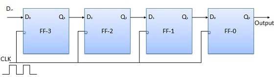
Serial In - Serial Out (SISO) Shift Register
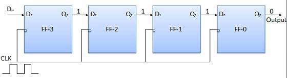
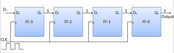
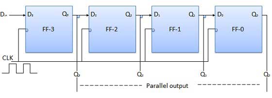
Let all the flip-flop be initially in the reset condition i.e. Q3 = Q2 = Q1 = Q0 = 0. If an entry of a four bit binary number 1 1 1 1 is made into the register, this number should be applied to Din bit with the LSB bit applied first. The D input of FF-3 i.e. D3 is connected to serial data input Din. Output of FF-3 i.e. Q3 is connected to the input of the next flip-flop i.e. D2 and so on.
Block Diagram
Operation
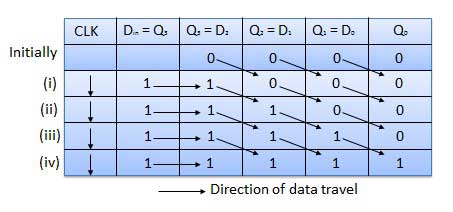
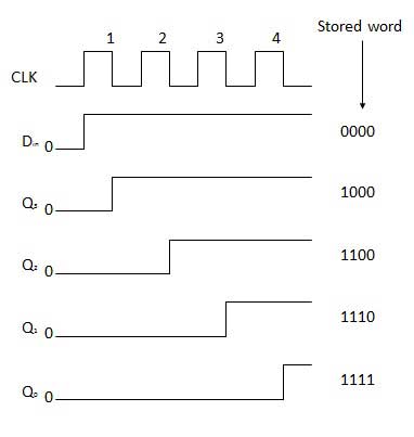
Before application of clock signal, let Q3 Q2 Q1 Q0 = 0000 and apply LSB bit of the number to be entered to Din. So Din = D3 = 1. Apply the clock. On the first falling edge of clock, the FF-3 is set, and stored word in the register is Q3 Q2 Q1 Q0 = 1000.
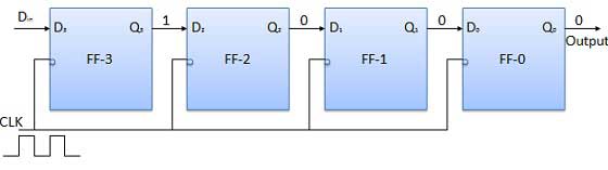
Apply the next bit to Din. So Din = 1. As soon as the next negative edge of the clock hits, FF-2 will set and the stored word change to Q3 Q2 Q1 Q0 = 1100.
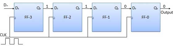
Apply the next bit to be stored i.e. 1 to Din. Apply the clock pulse. As soon as the third negative clock edge hits, FF-1 will be set and output will be modified to Q3 Q2 Q1 Q0 = 1110.
Similarly with Din = 1 and with the fourth negative clock edge arriving, the stored word in the register is Q3 Q2 Q1 Q0 = 1111.
Truth Table
Waveforms
Serial In - Parallel Out (SIPO) Shift Register
- In such types of operations, the data is entered serially and taken out in parallel fashion.
- Data is loaded bit by bit. The outputs are disabled as long as the data is loading.
- As soon as the data loading gets completed, all the flip-flops contain their required data, the outputs are enabled so that all the loaded data is made available over all the output lines at the same time.
- 4 clock cycles are required to load a four bit word. Hence the speed of operation of SIPO mode is same as that of SISO mode.
Block Diagram
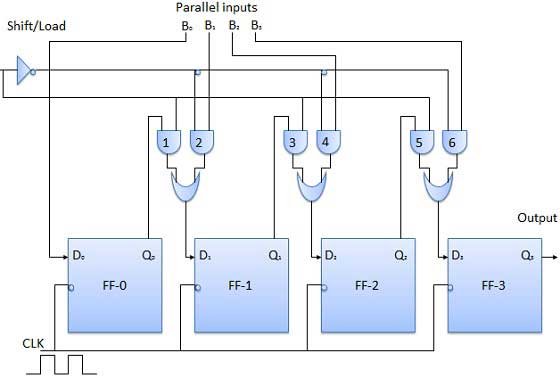
Parallel In - Serial Out (PISO) Shift Register
- Data bits are entered in parallel fashion.
- The circuit shown below is a four bit parallel input serial output register.
- Output of previous Flip Flop is connected to the input of the next one via a combinational circuit.
- The binary input word B0, B1, B2, B3 is applied though the same combinational circuit.
- There are two modes in which this circuit can work namely - shift mode or load mode.
Load Mode
When the shift/load bar line is low (0), the AND gate 2, 4 and 6 become active they will pass B1, B2, B3 bits to the corresponding flip-flops. On the low going edge of clock, the binary input B0, B1, B2, B3 will get loaded into the corresponding flip-flops. Thus parallel loading takes place.
Shift Mode
When the shift/load bar line is low (1), the AND gate 2, 4 and 6 become inactive. Hence the parallel loading of the data becomes impossible. But the AND gate 1,3 and 5 become active. Therefore the shifting of data from left to right bit by bit on application of clock pulses. Thus the parallel in serial out operation takes place.
Block Diagram
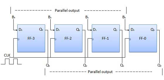
Parallel In - Parallel Out (PIPO) Shift Register
In this mode, the 4 bit binary input B0, B1, B2, B3 is applied to the data inputs D0, D1, D2, D3 respectively of the four flip-flops. As soon as a negative clock edge is applied, the input binary bits will be loaded into the flip-flops simultaneously. The loaded bits will appear simultaneously to the output side. Only clock pulse is essential to load all the bits.
Block Diagram
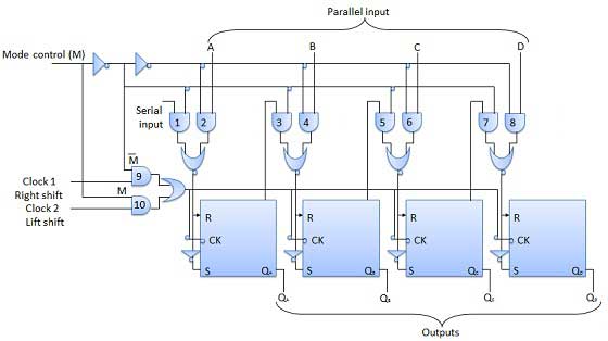
Bidirectional Shift Register
- If a binary number is shifted left by one position then it is equivalent to multiplying the original number by 2. Similarly if a binary number is shifted right by one position then it is equivalent to dividing the original number by 2.
- Hence if we want to use the shift register to multiply and divide the given binary number, then we should be able to move the data in either left or right direction.
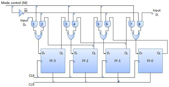
- Such a register is called bi-directional register. A four bit bi-directional shift register is shown in fig.
- There are two serial inputs namely the serial right shift data input DR, and the serial left shift data input DL along with a mode select input (M).
Block Diagram
Operation
| Sr.No | Condition | Operation |
|---|---|---|
| 1 | With M = 1 − Shift right operation |
If M = 1, then the AND gates 1, 3, 5 and 7 are enabled whereas the remaining AND gates 2, 4, 6 and 8 will be disabled. The data at DR is shifted to right bit by bit from FF-3 to FF-0 on the application of clock pulses. Thus with M = 1 we get the serial right shift operation. |
| 2 | With M = 0 − Shift left operation |
When the mode control M is connected to 0 then the AND gates 2, 4, 6 and 8 are enabled while 1, 3, 5 and 7 are disabled. The data at DL is shifted left bit by bit from FF-0 to FF-3 on the application of clock pulses. Thus with M = 0 we get the serial right shift operation. |
Universal Shift Register
A shift register which can shift the data in only one direction is called a uni-directional shift register. A shift register which can shift the data in both directions is called a bi-directional shift register. Applying the same logic, a shift register which can shift the data in both directions as well as load it parallely, is known as a universal shift register. The shift register is capable of performing the following operation −
- Parallel Loading
- Left Shifting
- Right Shifting
The mode control input is connected to logic 1 for parallel loading operation whereas it is connected to 0 for serial shifting. With mode control pin connected to ground, the universal shift register acts as a bi-directional register. For serial left operation, the input is applied to the serial input which goes to AND gate-1 shown in figure. Whereas for the shift right operation, the serial input is applied to D input.
Block Diagram