
Article Categories
- All Categories
-
 Data Structure
-
 Networking
-
 RDBMS
RDBMS
-
 Operating System
-
 Java
Java
-
 MS Excel
-
 iOS
iOS
-
 HTML
HTML
-
 CSS
CSS
-
 Android
-
 Python
-
 C Programming
-
 C++
C++
-
 C#
C#
-
 MongoDB
-
 MySQL
MySQL
-
 Javascript
-
 PHP
PHP
-
 Economics & Finance
What is control of Register and Memory in Computer Architecture?
The control inputs to registers and memory are −
- Load (LD) − When it is enabled, the content from the source register or memory can be transferred to/from the bus.
- Increment (INR) − It can increment the register by 1.
- Clear (CLR) − It can clear the register.
The figure shows a scheme for the control of registers and memory.
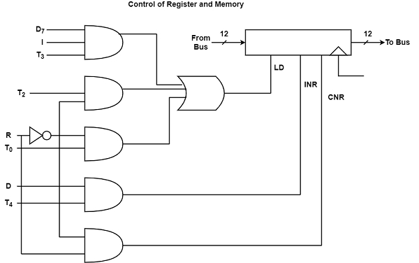
As shown in the diagram, all the register transfer statements are checked originally which modifies the content of AR.
The instructions are as follows −
| R′T0: | AR ← PC |
| R′T2: | AR ← IR(0 − 11) |
| D′7IT3 : | AR ← M[AR] |
| RT0: | AR ← 0 |
| D5T4: | AR ← AR + 1 |
The first three statements determine the transfer of data from a register or memory to AR. The content of the source register or memory is located on the bus and the content of the bus is transferred into AR by enabling its LD control input. The fourth statement clears AR to 0. The final statement increments AR by 1.
The control functions can be combined into three Boolean expressions as follows −
| LD(AR): | R′T0 + R′T2 + D′7 IT3 |
| CLR(AR): | RT0 |
| INR(AR): | D5T4 |
where LD(AR) is the load input of AR, CLR(AR) is the clear input of AR, and INR(AR) is the increment input of AR. The control gate logic associated with AR is displayed in the figure.
Similarly, we can change the control gates for the other registers and the logic required to control the read and write inputs of memory. The logic gates associated with the read input of memory are changed by checking the table to find the statements that determine a read operation. The read operation is recognized from the symbol←M [AR].
Read = R′T1 + D′7 IT3 + (D0 + D1 + D2 + D6 )T4
The output of the logic gates that execute the Boolean expression should be linked to the read input of memory.

2K+ Views
