
Article Categories
- All Categories
-
 Data Structure
-
 Networking
-
 RDBMS
RDBMS
-
 Operating System
-
 Java
Java
-
 MS Excel
-
 iOS
iOS
-
 HTML
HTML
-
 CSS
CSS
-
 Android
-
 Python
-
 C Programming
-
 C++
C++
-
 C#
C#
-
 MongoDB
-
 MySQL
MySQL
-
 Javascript
-
 PHP
PHP
-
 Economics & Finance
What is the configuration of memory subsystem in computer architecture?
There is the following technique for joining memory chips to form a memory subsystem. Two or more chips can be combined to generate a memory with more bits per location. This is done by linking the corresponding address and control signals of the chips and linking their data pins to various bits of the data bus.
For example, two 8 x 2 chips can be combined to generate an 8 x 4 memory as displayed in the figure. Both chips get the equal three address inputs from the bus, and the same chip enables and output enables signals.
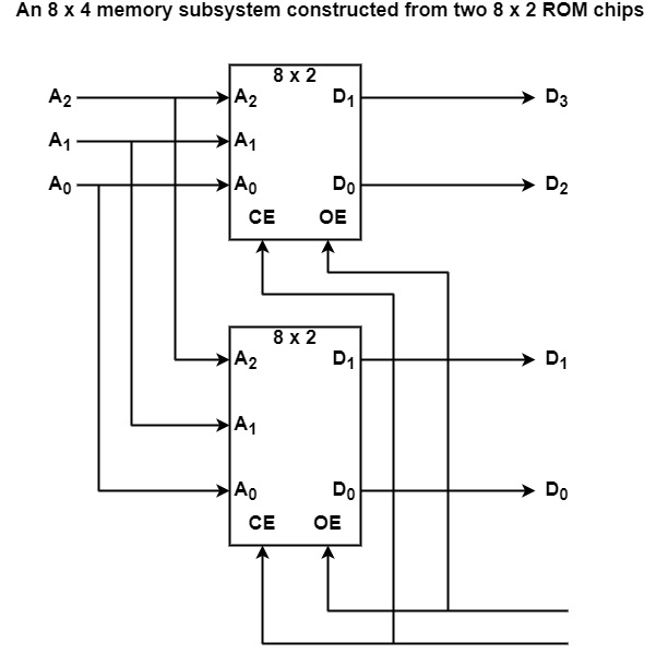
The data chips of the first chips are linked to bits 3 and 2 of the data bus, and those of the other chips are linked to bits 1 and 0. When the CPU reads data, it locates the address on the address bus. Both chips read in address bits A2, A1, and A0 and implement their internal decoding.
If the CE and OE signals are activated, the chips output their data onto the four bits of the data bus. Because the address and enable signals are equal for both chips, either both chips and neither chip is active at any given time. The device never has only one of the two active. For this reason, they facilitate as only a single 8 x 4 chip at least until the CPU is concerned.
Instead of generating wider words, chips can be combined to make more words. The similar two 8 x 2 chips could alternatively be configured as a 16 x 2 memory subsystem. The upper chip is configured as memory locations 0 to 7 (0000 to 0111) and the lower chip as locations 8 to 15 (1000 to 1111).
The upper chip always has A3=0 and the lower chip has A3=1. This difference can choose one of the two chips. When A3=0, the upper chip is enabled and the lower chip is disabled. The output enables can be linked, because only the chip that is enabled with output data. Both chips correspond to similar data bits, both are linked to D1 and D0 of the data bus.
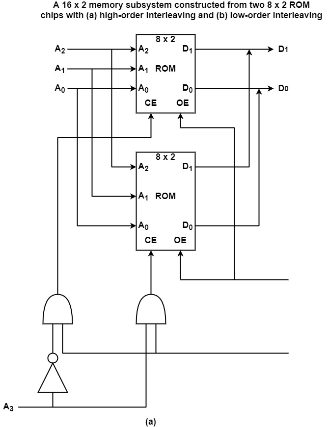
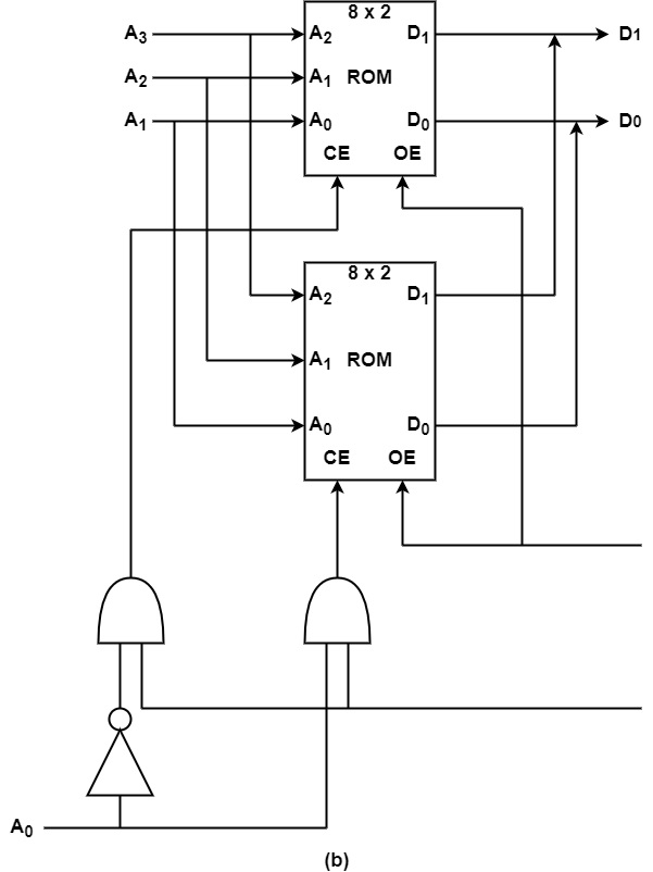
This configuration uses high-order interleaving. All memory locations inside a chip are contiguous within system memory. Consider the configuration displayed in figure (b) which uses low-order interleaving. The upper chip is enabled when A0=0, or by addresses XXX0, in this case, 0, 2, 4, 6, 8, 10,12, and 14. The lower chip is enabled when A0=1, which is correct for addresses 1, 3, 5, 7, 9, 11, 13, and 15.

2K+ Views
