
Article Categories
- All Categories
-
 Data Structure
-
 Networking
-
 RDBMS
RDBMS
-
 Operating System
-
 Java
Java
-
 MS Excel
-
 iOS
iOS
-
 HTML
HTML
-
 CSS
CSS
-
 Android
-
 Python
-
 C Programming
-
 C++
C++
-
 C#
C#
-
 MongoDB
-
 MySQL
MySQL
-
 Javascript
-
 PHP
PHP
-
 Economics & Finance
Program memory structure of Intel 8051
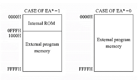
We have already discussed that the 8051 microcontroller has the internal program memory. In this chip, there is EA pin. It indicates the External Access. So by using this pin, we can check whether the internal program memory is used or not. So when there is a low signal in this pin, the internal 4K bytes of program memory is not used, but in this situation, it can access only the ROM.
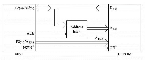
When we are trying to access the external data memory, then the read RD or write WR will be the output from 8051. So for reading the data from external sources, there PSEN (Program Strobe Enable) pin. This is an active low output pin. When this pin is active low, it indicates that the microcontroller reads from the external ROM. The 16-bit ROM address will be floated on Port 2 (MS Byte) and Port 0 (LS Byte). The program code is received on Port 0 pins.
So there is two case of accessing the program memory. The first case is when EA is low, and the second case is when EA is high. For the low state of EA, it can access the entire external memory from location 0000H to FFFFH. And in the second case (EA = 1). In this case, the internal memory is accessed by the address 0000H to 0FFFH. And also the external memory is accessed from location 1000H to FFFFH.
The external program memory address is always 16-bit address. If the memory is very small compared to 64KB memory, then also the address will be 16-bit. So when we use the external memory, we cannot use the Port0 and Port 2 as IO ports. The instruction execution times are not depending on the on-chip ROM or external EPROMs
So the structure of external program memory interfacing is like below

3K+ Views
