
Article Categories
- All Categories
-
 Data Structure
-
 Networking
-
 RDBMS
RDBMS
-
 Operating System
-
 Java
Java
-
 MS Excel
-
 iOS
iOS
-
 HTML
HTML
-
 CSS
CSS
-
 Android
-
 Python
-
 C Programming
-
 C++
C++
-
 C#
C#
-
 MongoDB
-
 MySQL
MySQL
-
 Javascript
-
 PHP
PHP
-
 Economics & Finance
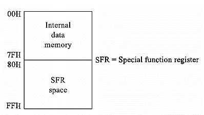
Internal Data Memory Organization of Intel 8051
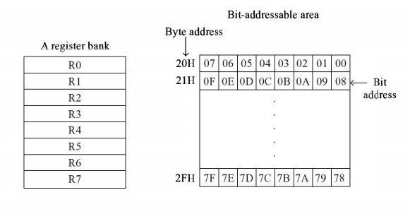
The internal data memory of 8051 is divided into two groups. These are a set of eight registers and a scratch pad memory. These eight registers are R0 toR7. The address range 00H to 07H is used to access the registers, and the rest are scratch pad memory.
8051 Provides four register bank, but only one register bank can be used at any point in time. To select the register bank, two bits of PSW (Program Status Word) are used.
So the following addressing can be used to select register banks.
| Address Range | Register Bank |
|---|---|
| 00H to 07H | Register Bank 0 |
| 08H to 0FH | Register Bank 1 |
| 10H to 17H | Register Bank 2 |
| 18H to 1FH | Register Bank 3 |
The concept of four register banks is very useful. For servicing the interrupts, this feature is very good. The interrupt program can use one bank, and the interrupt Service Subroutine (ISS) can access another bank for better performance. As there are four banks, so for nested interrupts these can be used
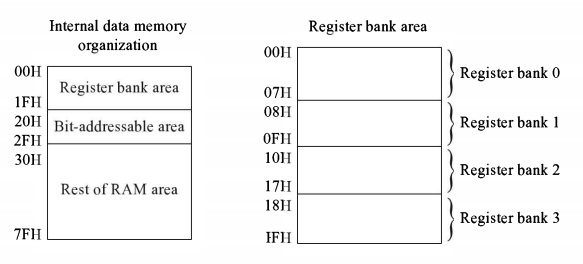
When all of the register banks are being used, the scratch pad area will be 20H to 7FH. But from 20H to 2FH (16 bytes or 128 bits) can be used as bit addressable RAM. By using some simple instructions with 8-bit memory address we can check the bit addressing. For an example the instruction CLR 6FH, using this instruction it clears the location 6FH. As we know the8-bit address can locate 256 different locations, but here only128-bits are addressable. Another section of bit addressable locations is 80H to FFH. The remaining locations (30H to 7EH) of the RAM can be used to store variable data and stack.
Stack Area
The stack area in 8051always can be implemented in the internal data memory. Here the stack pointer (SP) is an only 8-bit register, because the internal RAM area is only in range 00H to 7FH, and when all register banks are being used, the stack location will be in range 30H to 7FH. So in such a case, the SP will be initialized with 2FH.
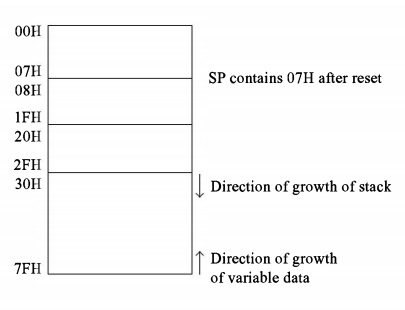
The stack pointer SP increases before each PUSH operation and decreases after each pop instruction.
When the 8051 is reset, the Stack Pointer will point to 07H. It means the location 08H to 7FHcan be used as a stack. We are assuming that the register bank 0 is in use and 20H to 27H are not like bit-addressable area.

48K+ Views
