
Article Categories
- All Categories
-
 Data Structure
-
 Networking
-
 RDBMS
RDBMS
-
 Operating System
-
 Java
Java
-
 MS Excel
-
 iOS
iOS
-
 HTML
HTML
-
 CSS
CSS
-
 Android
-
 Python
-
 C Programming
-
 C++
C++
-
 C#
C#
-
 MongoDB
-
 MySQL
MySQL
-
 Javascript
-
 PHP
PHP
-
 Economics & Finance
AD7-0 pins in 8085 Microprocessor
The Intel 8085 is an 8-bit microprocessor produced by Intel and introduced in 1976. It is a software-binary compatible with the more-famous Intel 8080 with only two minor instructions added to support its added interrupt and serial input/output features. When the 8085desires to receive 8-bit information, it receives it on these eight pins AD7, AD6,…, AD0. These eight pins are collectively called AD7-0. They are called basically “Address Data”. When the 8085 desires to send out 8-bit information, it sends it out on these same pins. these pins are bi-directional pins.
The same lines are used for both receiving information and sending out information because, at any instant of time, the processor is either receiving or sending out information, but not both. They are decided by the signals sent out on RD`and WR`pins.
RD` and WR` Pins– RD `stands for “ Read*”. RD`is an active low output signal.
RD`is pin number 32 of 8085. When RD`= 0, AD7-0 pins are input pins. When RD`= 1, it means the 8085 is not reading information.
WR`stands for “Write”. WR` is an active low output signal. WR` is pin number 31 of 8085. When WR`= 0, AD7-0 pin sare output pins. When WR`= 1, it means the 8085 is not writing or sending out information.
If the control unit in the 8085 sends out logic 1 on both RD`and WR` simultaneously, it means that the 8085 is not interested in reading or writing at that moment.
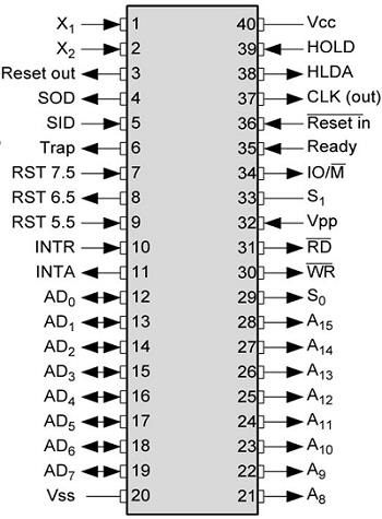
Fig: Pin diagram of 8085
Let us consider this following example and also the voltage levels at AD7, AD6,…, AD0 pins. If we consider instruction MVIE, ABH then it means that ABH will is moved or copied to the register E. And, as a result, the previous value of E will get overwritten.
| Address |
Hex Codes |
Mnemonic |
Comment |
|---|---|---|---|
| 2000 |
1E |
MVIE, ABH |
E ← ABH |
| 2001 |
AB |
|
ABHas operand |
This instruction will have seven T-states as shown below.
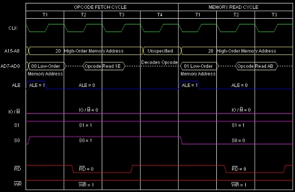
Summary − So this instruction MVIE, ABH requires 2-Bytes, 2-Machine Cycles Opcode Fetch and Memory Read) and 7 T-States for execution as shown in the timing diagram.

1K+ Views
