- CUDA - Home
- CUDA - Introduction
- CUDA - Introduction to the GPU
- Fixed Functioning Graphics Pipelines
- CUDA - Key Concepts
- Keywords and Thread Organization
- CUDA - Installation
- CUDA - Matrix Multiplication
- CUDA - Threads
- CUDA - Performance Considerations
- CUDA - Memories
- CUDA - Memory Considerations
- Reducing Global Memory Traffic
- CUDA - Caches
CUDA - Quick Guide
Cuda - Introduction
CUDA − Compute Unified Device Architecture. It is an extension of C programming, an API model for parallel computing created by Nvidia. Programs written using CUDA harness the power of GPU. Thus, increasing the computing performance.
Parallelism in the CPU
Gordon Moore of Intel once famously stated a rule, which said that every passing year, the clock frequency of a semiconductor core doubles. This law held true until recent years. Now, as the clock frequencies of a single core reach saturation points (you will not find a single core CPU with a clock frequency of say, 5GHz, even after 2 years from now), the paradigm has shifted to multi-core and many-core processors.
In this chapter, we will study how parallelism is achieved in CPUs. This chapter is an essential foundation to studying GPUs (it helps in understanding the key differences between GPUs and CPUs).
Following are the five essential steps required for an instruction to finish −
- Instruction fetch (IF)
- Instruction decode (ID)
- Instruction execute (Ex)
- Memory access (Mem)
- Register write-back (WB)
This is a basic five-stage RISC architecture.
There are multiple ways to achieve parallelism in the CPU. First, we will discuss about ILP (Instruction Level Parallelism), also known as pipelining.
Pipelining
A CPU pipeline is a series of instructions that a CPU can handle in parallel per clock. A basic CPU with no ILP will execute the above five steps sequentially. In fact, any CPU will do that. It will first fetch the instructions, decode them, execute them, then access the RAM, and then write-back to the registers. Thus, it needs at least five CPU cycles to execute an instruction. During this process, there are parts of the chip that are sitting idle, waiting for the current instruction to finish. This is highly inefficient and this is exactly what instruction pipelining tries to address. Instead now, in one clock cycle, there are many steps of different instructions that execute in parallel. Thus the name, Instruction Level Parallelism.
The following figure will help you understand how Instruction Level Parallelism works −
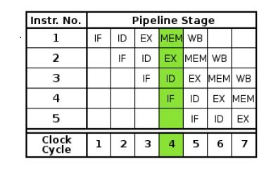
Using instruction pipelining, the instruction throughput has increased. Now, we can process many instructions in one-clock cycle. But for ILP, the resources of a chip would have been sitting idle.
In a pipe-lined chip, the instruction throughput increased. Initially, one instruction completed after every 5 cycles. Now, at the end of each cycle (from the 5th cycle onwards, considering each step takes 1 cycle), we get a completed instruction.
Note that in a non-pipelined chip, where it is assumed that the next instruction begins only when the current has finished, there is no data hazard. But since such is not the case with a pipelined chip, hazards may arise. Consider the situation below −
- I1 − ADD 1 to R5
- I2 − COPY R5 to R6
Now, in a pipeline processor, I1 starts at t1, and finishes at t5. I2 starts at t2 and finishes at t6. 1 is added to R5 at t5 (at the WB stage). The second instruction reads the value of R5 at its second step (at time t3). Thus, it will not fetch the update value, and this presents a hazard.
Modern compilers decode high-level code to low-level code, and take care of hazards.
Superscalar
ILP is also implemented by implementing a superscalar architecture. The primary difference between a superscalar and a pipelined processor is (a superscalar processor is also pipeline) that the former uses multiple execution units (on the same chip) to achieve ILP whereas the latter divides the EU in multiple phases to do that. This means that in superscalar, several instructions can simultaneously be in the same stage of the execution cycle. This is not possible in a simple pipelined chip. Superscalar microprocessors can execute two or more instructions at the same time. They typically have at least 2 ALUs.
Superscalar processors can dispatch multiple instructions in the same clock cycle. This means that multiple instructions can be started in the same clock cycle. If you look at the pipelines architecture above, you can observe that at any clock cycle, only one instruction is dispatched. This is not the case with superscalars. But we have only one instruction counter (in-flight, multiple instructions are tracked). This is still just one process.
Take the Intel i7 for instance. The processor boasts of 4 independent cores, each implementing the full x86 ISA. Each core is hyper-threaded with two hardware cores.
Hyper-threading is a dope technology, proprietary to Intel, using which the operating system see a single core as two virtual cores, for increasing the number of hardware instructions in the pipeline (note that not all operating systems support HT, and Intel recommends that in such cases, HT be disabled). So, the Intel i7 has a total of 8 hardware threads.
SMT
HT is just a technology to utilize a processor core better. Many a times, a processor core is utilizing only a fraction of its resources to execute instructions. What HT does is that it takes a few more CPU registers, and executes more instructions on the part of the core that is sitting idle. Thus, one core now appears as two core. It is to be considered that they are not completely independent. If both the cores need to access the CPU resource, one of them ends up waiting. That is the reason why we cannot replace a dual-core CPU with a hyper-threaded, single core CPU. A dual core CPU will have truly independent, out-of-order cores, each with its own resources. Also note that HT is Intels implementation of SMT (Simultaneous Multithreading). SPARC has a different implementation of SMT, with identical goals.
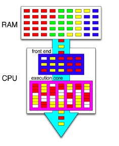
The pink box represents a single CPU core. The RAM contains instructions of 4 different programs, indicated by different colors. The CPU implements the SMT, using a technology similar to hyper-threading. Hence, it is able to run instructions of two different programs (red and yellow) simultaneously. White boxes represent pipeline stalls.
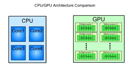
So, there are multi-core CPUs. One thing to notice is that they are designed to fasten-up sequential programs. A CPU is very good when it comes to executing a single instruction on a single datum, but not so much when it comes to processing a large chunk of data. A CPU has a larger instruction set than a GPU, a complex ALU, a better branch prediction logic, and a more sophisticated caching/pipeline schemes. The instruction cycles are also a lot faster.
CUDA - Introduction to the GPU
The other paradigm is many-core processors that are designed to operate on large chunks of data, in which CPUs prove inefficient. A GPU comprises many cores (that almost double each passing year), and each core runs at a clock speed significantly slower than a CPUs clock. GPUs focus on execution throughput of massively-parallel programs. For example, the Nvidia GeForce GTX 280 GPU has 240 cores, each of which is a heavily multithreaded, in-order, single-instruction issue processor (SIMD − single instruction, multiple-data) that shares its control and instruction cache with seven other cores. When it comes to the total Floating Point Operations per Second (FLOPS), GPUs have been leading the race for a long time now.
GPUs do not have virtual memory, interrupts, or means of addressing devices such as the keyboard and the mouse. They are terribly inefficient when we do not have SPMD (Single Program, Multiple Data). Such programs are best handled by CPUs, and may be that is the reason why they are still around. For example, a CPU can calculate a hash for a string much, much faster than a GPU, but when it comes to computing several thousand hashes, the GPU wins. As of data from 2009, the ratio b/w GPUs and multi-core CPUs for peak FLOP calculations is about 10:1. Such a large performance gap forces the developers to outsource their data-intensive applications to the GPU.
GPUs are designed for data intensive applications. This is emphasized-upon by the fact that the bandwidths of GPU DRAM has increased tremendously by each passing year, but not so much in case of CPUs. Why GPUs adopt such a design and CPUs do not? Well, because GPUs were originally designed for 3D rendering, which requires holding large amount of texture and polygon data. Caches cannot hold such large amount of data, and thus, the only design that would have increased rendering performance was to increase the bus width and the memory clock. For example, the Intel i7, which currently supports the largest memory bandwidth, has a memory bus of width 192b and a memory clock upto 800MHz. The GTX 285 had a bus width of 512b, and a memory clock of 1242 MHz.
CPUs also would not benefit greatly from an increased memory bandwidth. Sequential programs typically do not have a working set of data, and most of the required data can be stored in L1, L2 or L3 cache, which are faster than any RAM. Moreover, CPU programs generally have more random memory access patterns, unlike massively-parallel programs, that would not derive much benefit from having a wide memory bus.
GPU Design
Here is the architecture of a CUDA capable GPU −
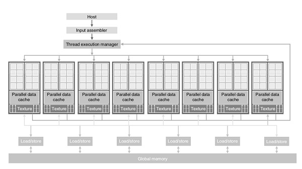
There are 16 streaming multiprocessors (SMs) in the above diagram. Each SM has 8 streaming processors (SPs). That is, we get a total of 128 SPs. Now, each SP has a MAD unit (Multiply and Addition Unit) and an additional MU (Multiply Unit). The GT200 has 240 SPs, and exceeds 1 TFLOP of processing power.
Each SP is massively threaded, and can run thousands of threads per application. The G80 card supports 768 threads per SM (note: not per SP). Since each SM has 8 SPs, each SP supports a maximum of 96 threads. Total threads that can run: 128 * 96 = 12,228. This is why these processors are called massively parallel.
The G80 chips has a memory bandwidth of 86.4GB/s. It also has an 8GB/s communication channel with the CPU (4GB/s for uploading to the CPU RAM, and 4GB/s for downloading from the CPU RAM).
Memories
At this point, it becomes essential that we understand the difference between different types of memories.
DRAM stands for Dynamic RAM. It is the most common RAM found in systems today, and is also the slowest and the least expensive one. The RAM is named so because the information stored on it is lost, and the processor has to refresh it several times in a second to preserve data.
SRAMstands for Static RAM. This RAM does not need to be refreshed like DRAM, and it is significantly faster than DRAM (the difference in speeds comes from the design and the static nature of these RAMs). It is also called the microprocessor cache RAM.
So, if SRAM is faster than DRAM, why are DRAMs even used? The primary reason for this is that for the same amount of memory, SRAMs cost several times more than DRAMs. Therefore, processors do not have huge amount of cache memories. For example, the Intel 486 line microprocessor series has 8KB of internal SRAM cache (on-chip). This cache is used by the processor to store frequently used data, so that for each request, it does not have to access the much slower DRAM.
VRAM stands for Video RAM. It is quite similar to DRAM but with one major difference: it can be written to and read from simultaneously. This property is essential for better video performance. Using it, the video card can read data from VRAM and send it to the screen without having to wait for the CPU to finish writing it into the global memory. This property is of not much use in the rest of the computer, and therefore, VRAM are almost always used in video cards. Also, VRAMs are more expensive than DRAM, and this is one of the reasons why they have not replaced DRAMs yet.

CUDA - Fixed Functioning Graphics Pipelines
This kind of hardware was popular from the early 1980s to the late 1990s. These were fixed-function pipelines that were configurable, but not programmable. Modern GPUs are shader-based and programmable.
The fixed-function pipeline does exactly what the name suggests; its functionality is fixed. So, for example, if the pipeline contains a list of methods to rasterize geometry and shade pixels, that is pretty much it. You cannot add any more methods. Although these pipelines were good at rendering scenes, they enshrine certain deficiencies. In broad terms, you can perform linear transformations and then rasterize by texturing, interpolate a color across a face by combinations and permutations of those things. But what when you wanted to perform things that the pipeline could not do?
In modern GPUs, all the pipelines are generic, and can run any type of GPU assembler code. In recent time, the number of functions of the pipeline are many - they do vertex mapping, and color calculation for each pixel, they also support geometry shader (tessellation), and even compute shaders (where the parallel processor is used to do a non-graphics job).
Fixed function pipelines are limited in their capabilities, but are easy to design. They are not used much in todays graphics systems. Instead, programmable pipelines using OpenGL or DirectX are the de-facto standards for modern GPUs.
The following image illustrates and describes a fixed-function Nvidia pipeline.
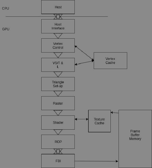
Let us understand the various stages of the pipeline now −
The CPU sends commands and data to the GPU host interface. Typically, the commands are given by application programs by calling an API function (from a list of many). A specialized Direct Memory Access (DMA) hardware is used by the host interface to fasten the transfer of bulk data to and fro the graphics pipeline.
In the GeForce pipeline, the surface of an object is drawn as a collection of triangles (the GeForce pipeline has been designed to render triangles). The finer the size of the triangle, the better the image quality (you can observe them in older games like the Tekken 3).
The vertex control stage receives parameterized triangle data from the host interface (which in-turn receives it from the CPU). Then comes the VT/T&;L stage. It stands for Vertex Shading, Transform and Lighting. This stage transforms vertices and assigns each vertex values for some parameters, such as colors, texture coordinates, normals and tangents. The pixel shader hardware does the shading (the vertex shader assigns a color value to each vertex, but coloring is done later).
The triangle setup stage is used to interpolate colors and other vertex parameters to those pixels that are touched by the triangle (the triangle setup stage actually determines the edge equations. It is the raster stage that interpolates).
The shader stage gives the pixel its final color. There are many methods to achieve this, apart form interpolations. Some of them include texture mapping, per-pixel lighting, reflections, etc.
Shading Using Interpolation
It is basically assigning a color to each vertex of a triangle on the surface (represented by polygon meshes, in our case, the polygon is a triangle), and linearly interpolating for each pixel covered by the triangle. There are many varieties to this, such as flat shading, Gouraud shading and Phong shading.
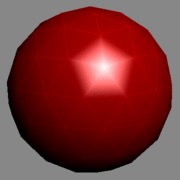
Let us now see shading using Gouraud shading. The triangle count is poor, and hence the poor performance of the specular highlight.
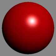
The same image rendered with a high triangle count.
Per-pixel Lighting
In this technique, illumination for each pixel is calculated. This results in a better quality image than an image that is shaded using interpolation. Most modern video games use this technique for increased realism and level of detail.
The ROP stage (Raster Operation) is used to perform the final rasterization steps on pixels. For example, it blends the color of overlapping objects for transparency and anti-aliasing effects. It also determines what pixels are occluded in a scene (a pixel is occluded when it is hidden by some other pixel in the image). Occluded pixels are simply discarded.
Reads and writes from the display buffer memory are managed by the last stage, that is, the frame buffer interface.
CUDA - Key Concepts
In this chapter, we will learn about a few key concepts related to CUDA. We will understand data parallelism, the program structure of CUDA and how a CUDA C Program is executed.
Data Parallelism
Modern applications process large amounts of data that incur significant execution time on sequential computers. An example of such an application is rendering pixels. For example, an application that converts sRGB pixels to grayscale. To process a 1920x1080 image, the application has to process 2073600 pixels.
Processing all those pixels on a traditional uniprocessor CPU will take a very long time since the execution will be done sequentially. (The time taken will be proportional to the number of pixels in the image). Further, it is very inefficient since the operation that is performed on each pixel is the same, but different on the data (SPMD). Since processing one pixel is independent of the processing of any other pixel, all the pixels can be processed in parallel. If we use 2073600 threads (workers) and each thread processes one pixel, the task can be reduced to constant time. Millions of such threads can be launched on modern GPUs.
As has already been explained in the previous chapters, GPU is traditionally used for rendering graphics. For example, per-pixel lighting is a highly parallel, and data-intensive task and a GPU is perfect for the job. We can map each pixel with a thread and they all can be processed in O(1) constant time.
Image processing and computer graphics are not the only areas in which we harness data parallelism to our advantage. Many high-performance algebra libraries today such as CU-BLAS harness the processing power of the modern GPU to perform data intensive algebra operations. One such operation, matrix multiplication has been explained in the later sections.
Program Structure of CUDA
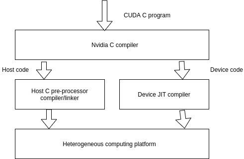
A typical CUDA program has code intended both for the GPU and the CPU. By default, a traditional C program is a CUDA program with only the host code. The CPU is referred to as the host, and the GPU is referred to as the device. Whereas the host code can be compiled by a traditional C compiler as the GCC, the device code needs a special compiler to understand the api functions that are used. For Nvidia GPUs, the compiler is called the NVCC (Nvidia C Compiler).
The device code runs on the GPU, and the host code runs on the CPU. The NVCC processes a CUDA program, and separates the host code from the device code. To accomplish this, special CUDA keywords are looked for. The code intended to run of the GPU (device code) is marked with special CUDA keywords for labelling data-parallel functions, called Kernels. The device code is further compiled by the NVCC and executed on the GPU.
Execution of a CUDA C Program
How does a CUDA program work? While writing a CUDA program, the programmer has explicit control on the number of threads that he wants to launch (this is a carefully decided-upon number). These threads collectively form a three-dimensional grid (threads are packed into blocks, and blocks are packed into grids). Each thread is given a unique identifier, which can be used to identify what data it is to be acted upon.
Device Global Memory and Data Transfer
As has been explained in the previous chapter, a typical GPU comes with its own global memory (DRAM- Dynamic Random Access Memory). For example, the Nvidia GTX 480 has DRAM size equal to 4G. From now on, we will call this memory the device memory.
To execute a kernel on the GPU, the programmer needs to allocate separate memory on the GPU by writing code. The CUDA API provides specific functions for accomplishing this. Here is the flow sequence −
After allocating memory on the device, data has to be transferred from the host memory to the device memory.
After the kernel is executed on the device, the result has to be transferred back from the device memory to the host memory.
The allocated memory on the device has to be freed-up. The host can access the device memory and transfer data to and from it, but not the other way round.
CUDA provides API functions to accomplish all these steps.
CUDA - Keywords and Thread Organization
In this chapter, we will discuss the keywords and thread organisation in CUDA.
The following keywords are used while declaring a CUDA function. As an example, while declaring the kernel, we have to use the __global__ keyword. This provides a hint to the compiler that this function will be executed on the device and can be called from the host.
| EXECUTED ON THE − | CALLABLE FROM − | |
|---|---|---|
| __device__ float function() | GPU (device) | CPU (host) |
| __global__ void function() | CPU (host) | GPU (device) | __host__float function() | GPU (device) | GPU (device) |
A Sample Cuda C Code
In this section, we will see a sample CUDA C Code.
void vecAdd(float* A, float* B, float* C,int N) {
   int size=N*sizeOf(float);
   float *d_A,*d_B,*d_C;
   cudaMalloc((void**)&;d_A,size);
This helps in allocating memory on the device for storing vector A. When the function returns, we get a pointer to the starting location of the memory.
cudaMemcpy(d_A,A,size,cudaMemcpyHostToDevice);
Copy data from host to device. The host memory contains the contents of vector A. Now that we have allocated space on the device for storing vector A, we transfer the contents of vector A to the device. At this point, the GPU memory has vector A stored, ready to be operated upon.
cudaMalloc((void**)&;d_B,size);
cudaMemcpy(d_B,B,size,cudaMemcpyHostToDevice);

//Similar to A
cudaMalloc((void**)&;d_C,size);
This helps in allocating the memory on the GPU to store the result vector C. We will cover the Kernel launch statement later.
cudaMemcpy(C,d_C,size,cudaMemcpyDeviceToHost);
After all the threads have finished executing, the result is stored in d_C (d stands for device). The host copies the result back to vector C from d_C.
cudaFree(d_A);
cudaFree(d_B);
cudaFree(d_C);
This helps to free up the memory allocated on the device using cudaMalloc().
This is how the above program works −
The above program adds the corresponding elements of two vectors X and Y, and stores the final result in a vector Z.
The device memory is allocated for storing the input vectors (X and Y) and the result vector (Z).
cudaMalloc() − This method is used to allocate memory on the host. in two parameters, the address of a pointer to the allocated object, and the size of the allocated object in terms of bytes.
cudaFree() − This method is used to release objects from device memory. It takes in the pointer to the freed object as parameter.
cudaMemcpy() − This API function is used for memory data transfer. It requires four parameters as input: Pointer to the destination, pointer to the source, amount of data to be copied (in bytes), and the direction of transfer.
CUDA Thread Organization
Threads in a grid execute the same kernel function. They have specific coordinates to distinguish themselves from each other and identify the relevant portion of data to process. In CUDA, they are organized in a two-level hierarchy: a grid comprises blocks, and each block comprises threads.
For all threads in a block, the block index is the same. The block index parameter can be accessed using the blockIdx variable inside a kernel. Each thread also has an associated index, and it can be accessed by using threadIdx variable inside the kernel. Note that blockIdx and threadIdx are built-in CUDA variables that are only accessible from inside the kernel.
In a similar fashion, CUDA also has gridDim and blockDim variables that are also built-in. They return the dimensions of the grid and block along a particular axis respectively. As an example, blockDim. x can be used to find how many threads a particular block has along the x axis.

Let us consider an example to understand the concept explained above. Consider an image, which is 76 pixels along the x axis, and 62 pixels along the y axis. Our aim is to convert the image from sRGB to grayscale. We can calculate the total number of pixels by multiplying the number of pixels along the x axis with the total number along the y axis that comes out to be 4712 pixels. Since we are mapping each thread with each pixel, we need a minimum of 4712 pixels. Let us take number of threads in each direction to be a multiple of 4. So, along the x axis, we will need at least 80 threads, and along the y axis, we will need at least 64 threads to process the complete image. We will ensure that the extra threads are not assigned any work.
Thus, we are launching 5120 threads to process a 4712 pixels image. You may ask, why the extra threads? The answer to this question is that keeping the dimensions as multiple of 4 has many benefits that largely offsets any disadvantages that result from launching extra threads. This is explained in a later section).
Now, we have to divide these 5120 threads into grids and blocks. Let each block have 256 threads. If so, then one possibility that of the dimensions each block are: (16,16,1). This means, there are 16 threads in the x direction, 16 in the y direction, and 1 in the z direction. We will be needing 5 blocks in the x direction (since there are 80 threads in total along the x axis), and 4 blocks in y direction (64 threads along the y axis in total), and 1 block in z direction. So, in total, we need 20 blocks. In a nutshell, the grid dimensions are (5,4,1) and the block dimensions are (16,16,1). The programmer needs to specify these values in the program. This is shown in the figure above.
dim3 dimBlock(5,4,1) − To specify the grid dimensions
dim3 dimGrid(ceil(n/16.0),ceil(m/16.0),1) − To specify the block dimensions.
kernelName<<<dimGrid,dimBlock>>>(parameter1, parameter2, ...) − Launch the actual kernel.
n is the number of pixels in the x direction, and m is the number of pixels in the y direction. ceil is the regular ceiling function. We use it because we never want to end up with less number of blocks than required. dim3 is a data structure, just like an int or a float. dimBlock and dimGrid are variables names. The third statement is the kernel launch statement. kernelName is the name of the kernel function, to which we pass the parameters: parameter1, parameter2, and so on. <<<>>> contain the dimensions of the grid and the block.
CUDA - Installation
In this chapter, we will learn how to install CUDA.
For installing the CUDA toolkit on Windows, youll need −
- A CUDA enabled Nvidia GPU.
- A supported version of Microsoft Windows.
- A supported version of Visual Studio.
- The latest CUDA toolkit.
Note that natively, CUDA allows only 64b applications. That is, you cannot develop 32b CUDA applications natively (exception: they can be developed only on the GeForce series GPUs). 32b applications can be developed on x86_64 using the cross-development capabilities of the CUDA toolkit. For compiling CUDA programs to 32b, follow these steps −
Step 1 − Add <installpath>\bin to your path.
Step 2 − Add -m32 to your nvcc options.
Step 3 − Link with the 32-bit libs in <installpath>\lib (instead of <installpath>\lib64).
You can download the latest CUDA toolkit from here.
Compatibility
| Windows version | Native x86_64 support | X86_32 support on x86_32 (cross) |
|---|---|---|
| Windows 10 | YES | YES |
| Windows 8.1 | YES | YES |
| Windows 7 | YES | YES |
| Windows Server 2016 | YES | NO |
| Windows Server 2012 R2 | YES | NO |
| Visual Studio Version | Native x86_64 support | X86_32 support on x86_32 (cross) |
|---|---|---|
| 2017 | YES | NO |
| 2015 | YES | NO |
| 2015 Community edition | YES | NO |
| 2013 | YES | YES |
| 2012 | YES | YES |
| 2010 | YES | YES |
As can be seen from the above tables, support for x86_32 is limited. Presently, only the GeForce series is supported for 32b CUDA applications. If you have a supported version of Windows and Visual Studio, then proceed. Otherwise, first install the required software.
Verifying if your system has a CUDA capable GPU − Open a RUN window and run the command − control /name Microsoft.DeviceManager, and verify from the given information. If you do not have a CUDA capable GPU, or a GPU, then halt.
Installing the Latest CUDA Toolkit
In this section, we will see how to install the latest CUDA toolkit.
Step 1 − Visit − https://developer.nvidia.com and select the desired operating system.
Step 2 − Select the type of installation that you would like to perform. The network installer will initially be a very small executable, which will download the required files when run. The standalone installer will download each required file at once and wont require an Internet connection later to install.
Step 3 − Download the base installer.
The CUDA toolkit will also install the required GPU drivers, along with the required libraries and header files to develop CUDA applications. It will also install some sample code to help starters. If you run the executable by double-clicking on it, just follow the on-screen directions and the toolkit will be installed. This is the graphical way of installation, and the downside of this method is that you do not have control on what packages to install. This can be avoided if you install the toolkit using CLI. Here is a list of possible packages that you can control −
| nvcc_9.1 | cuobjdump_9.1 | nvprune_9.1 | cupti_9.1 |
| demo_suite_9.1 | documentation_9.1 | cublas_9.1 | gpu-library-advisor_9.1 |
| curand_dev_9.1 | nvgraph_9.1 | cublas_dev_9.1 | memcheck_9.1 |
| cusolver_9.1 | nvgraph_dev_9.1 | cudart_9.1 | nvdisasm_9.1 |
| cusolver_dev_9.1 | npp_9.1 | cufft_9.1 | nvprof_9.1 |
| cusparse_9.1 | npp_dev_9.1 | cufft_dev_9.1 | visual_profiler_9.1 |
For example, to install only the compiler and the occupancy calculator, use the following command −
<PackageName>.exe -s nvcc_9.1 occupancy_calculator_9.1
Verifying the Installation
Follow these steps to verify the installation −
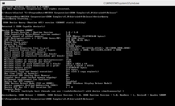
Step 1 − Check the CUDA toolkit version by typing nvcc -V in the command prompt.
Step 2 − Run deviceQuery.cu located at: C:\ProgramData\NVIDIA Corporation\CUDA Samples\v9.1\bin\win64\Release to view your GPU card information. The output will look like −
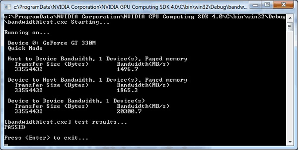
Step 3 − Run the bandWidth test located at C:\ProgramData\NVIDIA Corporation\CUDA Samples\v9.1\bin\win64\Release. This ensures that the host and the device are able to communicate properly with each other. The output will look like −
If any of the above tests fail, it means the toolkit has not been installed properly. Re-install by following the above instructions.
Uninstalling
CUDA can be uninstalled without any fuss from the Control Panel of Windows.
At this point, the CUDA toolkit is installed. You can get started by running the sample programs provided in the toolkit.
Setting-up Visual Studio for CUDA
For doing development work using CUDA on Visual Studio, it needs to be configured. To do this, go to − File → New | Project... NVIDIA → CUDA →. Now, select a template for your CUDA Toolkit version (We are using 9.1 in this tutorial). To specify a custom CUDA Toolkit location, under CUDA C/C++, select Common, and set the CUDA Toolkit Custom Directory.
CUDA - Matrix Multiplication
We have learnt how threads are organized in CUDA and how they are mapped to multi-dimensional data. Let us go ahead and use our knowledge to do matrix-multiplication using CUDA. But before we delve into that, we need to understand how matrices are stored in the memory. The manner in which matrices are stored affect the performance by a great deal.
2D matrices can be stored in the computer memory using two layouts − row-major and column-major. Most of the modern languages, including C (and CUDA) use the row-major layout. Here is a visual representation of the same of both the layouts −
| M0,0 | M0,1 | M0,2 | M0,3 |
| M1,0 | M1,1 | M1,2 | M1,3 |
| M2,0 | M2,1 | M2,2 | M2,3 |
| M3,0 | M3,1 | M3,2 | M3,3 |
Matrix to be stored
| M0,0 | M0,1 | M0,2 | M0,3 | M1,0 | M1,1 | M1,2 | M1,3 | M2,0 | M2,1 | M2,2 | M2,3 | M3,0 | M3,1 | M3,2 | M3,3 |
Row-major layout
Actual organization in memory −
| M0,0 | M1,0 | M2,0 | M3,0 | M0,1 | M1,1 | M2,1 | M3,1 | M0,2 | M1,2 | M2,2 | M3,2 | M0,3 | M1,3 | M2,3 | M3,3 |
Actual organization in memory −
Column-major layout
Actual organization in memory
Note that a 2D matrix is stored as a 1D array in memory in both the layouts. Some languages like FORTRAN follow the column-major layout.
Addressing
In row-major layout, element(x,y) can be addressed as: x*width + y. In the above example, the width of the matrix is 4. For example, element (1,1) will be found at position −
1*4 + 1 = 5 in the 1D array.
We will be mapping each data element to a thread. The following mapping scheme is used to map data to thread. This gives each thread its unique identity.
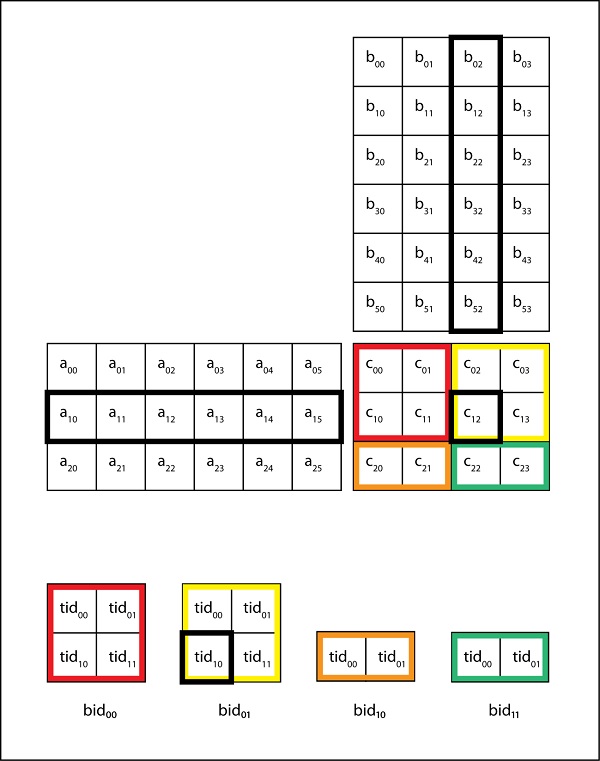
row=blockIdx.x*blockDim.x+threadIdx.x;
col=blockIdx.y*blockDim.y+threadIdx.y;
We know that a grid is made-up of blocks, and that the blocks are made up of threads. All threads in the same block have the same block index. Each coloured chunk in the above figure represents a block (the yellow one is block 0, the red one is block 1, the blue one is block 2 and the green one is block 3). So, for each block, we have blockDim.x=4 and blockDim.y=1. Let us find the unique identity of thread M(0,2). Since it lies in the yellow array, blockIdx.x=0 and threadIdx.x=2. So, we get: 0*4+2=2.
In the previous chapter, we noted that we often launch more threads than actually needed. To ensure that the extra threads do not do any work, we use the following if condition −
if(row<width && col<width) {
   then do work
}
The above condition is written in the kernel. It ensures that extra threads do not do any work.
Matrix multiplication between a (IxJ) matrix d_M and (JxK) matrix d_N produces a matrix d_P with dimensions (IxK). The formula used to calculate elements of d_P is −
d_Px,y = d_Mx,,k*d_Nk,y, for k=0,1,2,....width
A d_P element calculated by a thread is in blockIdx.y*blockDim.y+threadIdx.y row and blockIdx.x*blockDim.x+threadIdx.x column. Here is the actual kernel that implements the above logic.
__global__ void simpleMatMulKernell(float* d_M, float* d_N, float* d_P, int width)
{
This helps to calculate row and col to address what element of d_P will be calculated by this thread.
int row = blockIdx.y*width+threadIdx.y;
int col = blockIdx.x*width+threadIdx.x;
This ensures that the extra threads do not do any work.
if(row<width && col <width) {
   float product_val = 0
   for(int k=0;k<width;k++) {
      product_val += d_M[row*width+k]*d_N[k*width+col];
   }
   d_p[row*width+col] = product_val;
}
Let us now understand the above kernel with an example −
Let d_M be −
| 2 | 4 | 1 |
| 8 | 7 | 4 |
| 7 | 4 | 9 |
The above matrix will be stored as −
| 2 | 4 | 1 | 8 | 7 | 4 | 7 | 4 | 9 |
And let d_N be −
| 4 | 8 | 9 |
| 1 | 7 | 0 |
| 2 | 5 | 4 |
The above matrix will be stored as −
| 4 | 8 | 9 | 1 | 7 | 0 | 2 | 5 | 4 |
Since d_P will be a 3x3 matrix, we will be launching 9 threads, each of which will compute one element of d_P.
d_P matrix
| (0,0) | (0,1) | (0,2) |
| (1,0) | (1,1) | (1,2) |
| (2,0) | (2,1) | (2,2) |
Let us compute the (2,1) element of d_P by doing a dry-run of the kernel −
row=2;
col=1;
When (k=0)
product_val = 0 + d_M[2*3+0] * d_N[0*3+1]
product_val = 0 + d_M[6]*d_N[1] = 0+7*8=56
1st Iteration
product_val = 56 + d_M[2*3+1]*d_N[1*3+1]
product_val = 56 + d_M[7]*d_N[4] = 84
Final Iteration
product_val = 84+d_M[2*3+2]*d_N[2*3+1]
product_val = 84+d_M[8]*d_N[7] = 129
Now, we have −
d_P[7] = 129
CUDA - Threads
In this chapter, we will learn about the CUDA threads. To proceed, we need to first know how resources are assigned to blocks.
Resource Assignment to Blocks
Execution resources are assigned to threads per block. Resources are organized into Streaming Multiprocessors (SM). Multiple blocks of threads can be assigned to a single SM. The number varies with CUDA device. For example, a CUDA device may allow up to 8 thread blocks to be assigned to an SM. This is the upper limit, and it is not necessary that for any configuration of threads, a SM will run 8 blocks.
For example, if the resources of a SM are not sufficient to run 8 blocks of threads, then the number of blocks that are assigned to it is dynamically reduced by the CUDA runtime. Reduction is done on block granularity. To reduce the amount of threads assigned to a SM, the number of threads is reduced by a block.
In recent CUDA devices, a SM can accommodate up to 1536 threads. The configuration depends upon the programmer. This can be in the form of 3 blocks of 512 threads each, 6 blocks of 256 threads each or 12 blocks of 128 threads each. The upper limit is on the number of threads, and not on the number of blocks.
Thus, the number of threads that can run parallel on a CUDA device is simply the number of SM multiplied by the maximum number of threads each SM can support. In this case, the value comes out to be SM x 1536.
Synchronization between Threads
The CUDA API has a method, __syncthreads() to synchronize threads. When the method is encountered in the kernel, all threads in a block will be blocked at the calling location until each of them reaches the location.
What is the need for it? It ensure phase synchronization. That is, all the threads of a block will now start executing their next phase only after they have finished the previous one. There are certain nuances to this method. For example, if a __syncthreads statement, is present in the kernel, it must be executed by all threads of a block. If it is present inside an if statement, then either all the threads in the block go through the if statement, or none of them does.
If an if-then-else statement is present inside the kernel, then either all the threads will take the if path, or all the threads will take the else path. This is implied. As all the threads of a block have to execute the sync method call, if threads took different paths, then they will be blocked forever.
It is the duty of the programmer to be wary of such conditions that may arise.
Thread Scheduling
After a block of threads is assigned to a SM, it is divided into sets of 32 threads, each called a warp. However, the size of a warp depends upon the implementation. The CUDA specification does not specify it.
Here are some important properties of warps −
A warp is a unit of thread scheduling in SMs. That is, the granularity of thread scheduling is a warp. A block is divided into warps for scheduling purposes.
A SM is composed of many SPs (Streaming Processors). These are the actual CUDA cores. Normally, the number of CUDA cores in a SM is less than the total number of threads that are assigned to it. Thus the need for scheduling.
While a warp is waiting for the results of a previously executed long-latency operation (like data fetch from the RAM), a different warp that is not waiting and is ready to be assigned is selected for execution. This means that threads are always scheduled in a group.
If more than one warps are on the ready queue, then some priority mechanism can be used for assignment. One such method is the round-robin.
A warp consists of threads with consecutive threadIdx.x values. For example, threads of the first warp will have threads ids b/w 0 to 31. Threads of the second warp will have thread ids from 32-63.
All threads in a warp follow the SIMD model. SIMD stands for Single Instruction, Multiple Data. It is different when compared to SPMD. In SIMD, each thread is executing the same instruction of a kernel at any given time. But the data is always different.
Latency Tolerance
A lot of processor time goes waste if while a warp is waiting, another warp is not scheduled. This method of utilizing in the latency time of operations with work from other warps is called latency tolerance.
CUDA - Performance Considerations
In this chapter, we will understand the performance considerations of CUDA.
A poorly written CUDA program can perform much worse than intended. Consider the following piece of code −
for(int k=0; k<width; k++) {
   product_val += d_M[row*width+k] * d_N[k*width+col];
}
For every iteration of the loop, the global memory is accessed twice. That is, for two floating-point calculations, we access the global memory twice. One for fetching an element of d_M and one for fetching an element of d_N. Is it efficient? We know that accessing the global memory is terribly expensive the processor is simply wasting that time. If we can reduce the number of memory fetches per iteration, then the performance will certainly go up.
The CGMA ratio of the above program is 1:1. CGMA stands for Compute to Global Memory Access ratio, and the higher it is, the better the kernel performs. Programmers should aim to increase this ratio as much as it possible. In the above kernel, there are two floating-point operations. One is MUL and the other is ADD.
| YEAR | CPU (in GFLOPS) | GPU (in GFLOPS) |
|---|---|---|
| 2008 | 0-100 | 0-100 |
| 2009 | 0-100 | 300 |
| 2010 | 0-100 | 500 |
| 2011 | 0-100 | 800 |
| 2012 | 0-300 | 1200 |
| 2013 | 0-400 | 1500(K20) |
| 2014 | 500 | 1800(K40) |
| 2015 | 500-600 | 3000 (K80) |
| 2016 | 800 | 4000 (Pascal) |
| 2017 | 1300 | 7000 (Volta) |
Let the DRAM bandwidth be equal to 200G/s. Each single-precision floating-point value is 4B. Thus, in one second, no more than 50G single-precision floating-point values can be delivered. Since the CGMA ratio is 1:1, we can say that the maximum floating-point operations that the kernel will execute in 1 second is 50 GFLOPS (Giga Floating-point Operations per second). The peak performance of the Nvidia Titan X is 10157 GFLOPS for single-precision after boost. Compared to that 50GFLOPS is a minuscule number, and it is obvious that the above code will not harness the full potential of the card. Consider the kernel below −
__global__ void addNumToEachElement(float* M) {
   int index = blockIdx.x * blockDim.x + threadIdx.x;
   M[index] = M[index] + M[0];
}
The above kernel simply adds M[0] to each element of the array M. The number of global memory accesses for each thread is 3, while the total number of computations is 1 (ADD in the second instruction). The CGMA ratio is bad: . If we can eliminate the global memory access for M[0] for each thread, then the CGMA ratio will improve to 0.5. We will attain this by caching.
If the kernel does not have to fetch the value of M[0] from the global memory for every thread, then the CGMA ratio will increase. What actually happens is that the value of M[0] is cached aggressively by CUDA in the constant memory. The bandwidth is very high, and hence, fetching it from the constant memory is not a high-latency operation. Caching is used generously wherever possible by CUDA to improve performance.
Memory is often a bottleneck to achieving high performance in CUDA programs. No matter how fast the DRAM is, it cannot supply data at the rate at which the cores can consume it. It can be understood using the following analogy. Suppose that you are thirsty on a hot summer day, and someone offers you cold water, on the condition that you have to drink it using a straw. No matter how fast you try to suck the water in, only a specific quantity can enter your mouth per unit of time. In the case of GPUs, the cores are thirsty, and the straw is the actual memory bandwidth. It limits the performance here.
CUDA - Memories
Apart from the device DRAM, CUDA supports several additional types of memory that can be used to increase the CGMA ratio for a kernel. We know that accessing the DRAM is slow and expensive. To overcome this problem, several low-capacity, high-bandwidth memories, both on-chip and off-chip are present on a CUDA GPU. If some data is used frequently, then CUDA caches it in one of the low-level memories. Thus, the processor does not need to access the DRAM every time. The following figure illustrates the memory architecture supported by CUDA and typically found on Nvidia cards −
Device code
- R/W per-thread registers
- R/W per-thread local memory
- R/W per-block shared memory
- R/W per-grid global memory
- Read only per-grid constant memory
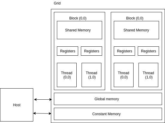
Host code
This helps in transferring data to/from per grid global and constant memories.
The global memory is a high-latency memory (the slowest in the figure). To increase the arithmetic intensity of our kernel, we want to reduce as many accesses to the global memory as possible. One thing to note about global memory is that there is no limitation on what threads may access it. All the threads of any block can access it. There are no restrictions, like there are in the case of shared memory or registers.
The constant memory can be written into and read by the host. It is used for storing data that will not change over the course of kernel execution. It supports short-latency, high-bandwidth, read-only access by the device when all threads simultaneously access the same location. There is a total of 64K constant memory on a CUDA capable device. The constant memory is cached. For all threads of a half warp, reading from the constant cache, as long as all threads read the same address, is no slower than reading from a register. However, if threads of the half-warp access different memory locations, the access time scales linearly with the number of different addresses read by all threads within the half-warp.
How does constant memory work?
For devices with CUDA capabilities 1.x, the following are the steps that are followed when a constant memory access is done by a warp −
The request is broken into two parts, one for each half-wrap. That is, two constant memory accesses will take place for a single request.
The request for each half-warp is split into as many discrete requests as there are different memory addresses in the initial request, decreasing the throughput by a factor equal to the number of separate requests. The cost increases linearly. If there is just one memory address that is accessed, then the access is as fast as it is from a register.
If there is a cache hit, then the resulting data is serviced at the bandwidth of the cache.
In case of a cache miss, the resulting data is serviced at the bandwidth of the DRAM.
The __constant__ keyword can be used to store a variable in constant memory. They are always declared as global variables.
Registers and shared-memory are on-chip memories. Variables that are stored in these memories are accessed at a very high speed in a highly parallel manner. A thread is allocated a set of registers, and it cannot access registers that are not parts of that set. A kernel generally stores frequently used variables that are private to each thread in registers. The cost of accessing variables from registers is less than that required to access variables from the global memory.
SM 2.0 GPUs support up to 63 registers per thread. If this limit is exceeded, the values will be spilled from local memory, supported by the cache hierarchy. SM 3.5 GPUs expand this to up to 255 registers per thread.
Shared Memory
All threads of a block can access its shared memory. Shared memory can be used for inter-thread communication. Each block has its own shared-memory. Just like registers, shared memory is also on-chip, but they differ significantly in functionality and the respective access cost.
While accessing data from the shared memory, the processor needs to do a memory load operation, just like accessing data from the global memory. This makes them slower than registers, in which the LOAD operation is not required. Since it resides on-chip, shared memory has shorter latency and higher bandwidth than global memory. Shared memory is also called scratchpad memory in computer architecture parlance.
Variable Lifetime
Lifetime of a variable tells the portion of the programs execution duration when it is available for use. If a variables lifetime is within the kernel, then it will be available for use only by the kernel code. An important point to note here is that multiple invocations of the kernel do not maintain the value of the variable across them.
Automatic Variables
Automatic variables are those variables for which a copy exists for each thread. In the matrix multiplication example, row and col are automatic variables. A private copy of row and col exists for each thread, and once the thread finishes execution, its automatic variables are destroyed.
The following table summarizes the lifetime, scope and memory of different types of CUDA variables −
| Variable declaration | Memory | Scope | Lifetime |
|---|---|---|---|
| Automatic variables other than arrays | Register | Thread | Kernel |
| Automatic array variables | Local | Thread | Kernel |
| __device__ __shared__ int sharedVar | Shared | Block | Kernel |
| __device__ int globalVar | Global | Grid | Application |
| __device__ __constant__ int constVar | Constant | Grid | Application |
Constant variables are stored in the global memory (constant memory), but are cached for efficient access. They can be accessed in a highly-parallel manner at high-speeds. As their lifetime equals the lifetime of the application, and they are visible to all the threads, declaration of constant variables must be done outside any function.
Memory as a Bottleneck
Although shared memory and registers are high-speed memories with huge bandwidth, they are available in limited amounts in a CUDA device. A programmer should be careful not to overuse these limited resources. The limited amount of these resources also caps the number of threads that can actually execute in parallel in a SM for a given application. The more resources a thread requires, the less the number of threads that can simultaneously reside in the SM. It is simply because there is a dearth of resources.
Let us suppose that each SM can accommodate upto 1536 threads and has 16,384 registers. To accommodate 1536 threads, each thread can use no more than 16,384/1536 = 10 registers. If each threads requires 12 registers, the number of threads that can simultaneously reside in the SM is reduced. Such reduction is done per block. If each block contains 128 threads, the reduction of threads will be done by reducing 128 threads at a time.
Shared memory usage can also limit the number of threads assigned to each SM. Suppose that a CUDA GPU has 16k/SM of shared memory. Suppose that each SM can support upto 8 blocks. To reach the maximum, each block must use no more than 2k of shared memory. If each block uses 5k of shared memory, then no more than 3 blocks can live in a SM.
CUDA - Memory Considerations
As we already know, CUDA applications process large chunks of data from the global memory in a short span of time. Hence, more often than not, limited memory bandwidth is a bottleneck to optimal performance.
In this chapter, we will discuss memory coalescing. It is one of the most important things that are taken into account while writing CUDA applications. Coalesced memory accesses improve the performance of your applications drastically.
Data bits in DRAM cells are stored in very weak capacitors that hold charge to distinguish between 1 and 0. A charge capacitor contains 1, and it shares its charge with a sensor that determines if it was sufficiently charged to represent a 1. This process is slow, and accessing a bit like this would be very inefficient. Instead, what actually happens is that many consecutive cells transfer their charges in parallel to increase bandwidth. There are multiple sensors present that detect charges on these cell in parallel. Whenever a location is accessed in the DRAM, data at locations adjacent to it are also accessed and supplied. Now, if that data were actually needed, then it is used and bandwidth is saved. Otherwise, it goes to waste.
We already know that threads in a warp execute the same instruction at any point in time. Let the instruction be LOAD (LD). If it so happens that the threads are accessing consecutive memory locations in the DRAM, then their individual requests can be coalesced into one. This is detected by the hardware dynamically, and saves a lot of DRAM bandwidth. When all threads of a warp access consecutive memory locations, it is the most optimal access pattern. For example, if thread 0 of the warp accesses location 0 of the DRAM, thread 1 accesses location 1, and so on, their requests will be merged into one. Such access patterns enable the DRAM to supply data close to their peak bandwidth.
Let us take our example of matrix-multiplication and see how the row-major layout gives rise to coalesced access pattern, ultimately leading to improved performance. Consider the matrix given below −
Matrix to be stored
| M0,0 | M0,1 | M0,2 | M0,3 |
| M1,0 | M1,1 | M1,2 | M1,3 |
| M2,0 | M2,1 | M2,2 | M2,3 |
| M3,0 | M3,1 | M3,2 | M3,3 |
Row major layout
| M0,0 | M0,1 | M0,2 | M0,3 | M1,0 | M1,1 | M1,2 | M1,3 | M2,0 | M2,1 | M2,2 | M2,3 | M3,0 | M3,1 | M3,2 | M3,3 |
Let us take the threads of a warp. Let each thread process a row. In the 0th iteration, all of them will be accessing the 0th element of each row. In the 1st iteration, the 1st element of each row, and in the 2nd iteration, the 2nd element. Now, since CUDA stores its matrices in row major layout, let us see the access pattern −
0th iteration
Elements accessed − M(0,0), M(1,0), M(2,0) and so on.
1th iteration
Elements accessed − M(0,1), M(1,1), M(2,1) and so on.
As you can see, the memory locations that are accessed in each loop are not consecutive. Hence, coalesced memory access will not be of much help here and optimal bandwidth is not achieved.
Let each thread now access the 0th element of each column. Let us see the access pattern now −
0th iteration
Elements accessed − M(0,0), M(0,1), M(0,2) and M(0,3) and so on.
1th iteration
Elements accessed − M(1,0), M(1,1), M(1,2) and M(1,3) and so on.
As you can see that in each iteration, consecutive memory locations are accessed, and hence, all these requests can be coalesced into a single one. This increases the kernel performance.
It may so happen that data are to be accessed in a non-favourable pattern. For example, while doing matrix multiplication, one of the matrices has to be read in a non-coalesced manner. The programmer has no choice here. So, what can instead be done is that one of the matrices can be loaded into the shared memory in a coalesced manner, and then it can be read in any pattern (row major or column major). Performance will not be affected much since the shared memory is an intrinsically high-speed memory that resides on-chip.
Here is a tiled kernel for matrix multiplication −
__global__ void MatrixMulTiled(float *Md, float *Nd, float *Pd, int width) {
   __shared__ float Mds[width_tile][width_tile];
   __shared__ float Nds[width_tile][width_tile];
   int bx = blockIdx.x;
   int by = blockIdx.y;
   int tx = threadIdx.x;
   int ty = threadIdx.y;

   //identify what pd element to work on
   int row = by * width_tile + ty;
   int col = bx * width_tile + tx;
   float product_val = 0;
   for(int m = 0; m < width/width_tile; m++) {

      //load the tiles
      Mds[ty][tx] = Md[row*width + (m*width_tile + tx)];
      Nds[ty][tx] = Nd[col*width + (m*width_tile + ty)];
      _syncthreads();
      for(int k=0; k < width_tile; k++) {
         product_val += Mds[ty][k] * Nds[k][tx];
      }
      pd[row][col] = product_val;
   }
}
CUDA - Reducing Global Memory Traffic
Resources in SM are dynamically partitioned and assigned to threads to support their execution. As has been explained in the previous chapter, the number of resources in SM are limited, and the higher the demands of a thread, the lower the number of threads that can actually run parallel inside the SM. Execution resources of SM include registers, shared memory, thread block slots and thread slots.
In the previous chapter, It has already been discussed that the current generation of CUDA devices support upto 1536 thread slots. That is, each SM can support no more than 1536 threads that can run in parallel. It has to be remembered that there is no capping on the number of thread blocks that can occupy a SM. They can be as many as would keep the total number of threads less than or equal to 1536 per SM. For example, there may be 3 blocks of 512 threads each, or 6 blocks of 256 threads each, or 12 blocks of 128 threads each.
This ability of CUDA to dynamically partition SM resources into thread blocks makes it the real deal. Fixed partitioning methods, in which each thread block receives a fixed number of execution resources regardless of its need leads to wasting of execution resources, which is not desired, as they are already at a premium. Dynamics partition has its own nuances. For example, suppose each thread block has 128 threads. This way, each SM will have 12 blocks. But we know that the current generation of CUDA devices support no more than 8 thread block slots per SM. Thus, out of 12, only 8 blocks will be allowed. This means that out of 1536 threads, only 1024 will be allocated to the SM. Thus, to fully utilize the available resources, we need to have at least 256 threads in each block.
In the matrix-multiplication example, consider that each SM has 16384 registers and each thread requires 10 registers. If we have 16x16 thread blocks, how many registers can run on each SM? The total number of registers needed per thread block = 256x10 = 2560 registers. This means that a maximum of 6 thread blocks (that need 15360 registers) can execute in a SM.
Thus, each SM can have a maximum of 6 x 256=1536 threads run on each SM. What if the number of registers required by each thread is 12? In that case, a thread block requires 256 x 12 = 3072 registers. Thus, we can have 5 blocks at maximum. This concludes that the maximum number of threads that can be allocated to a SM are 5 x 256 =1280.
It is to be noted that by using just two registers per thread extra, the warp parallelism reduces by 1/6.This is known as performance cliff and refers to a situation in which increasing the resource usage per thread even slightly leads to a large reduction in performance. The CUDA occupancy calculator (a program from Nvidia) can calculate the occupancy of each SM.
Reducing Traffic to the Global Memory Using Tiles
Let us consider an example of matrix-matrix multiplication once again. Our aim is to reduce the number of accesses to global memory to increase arithmetic intensity of the kernel. Let d_N and d_M be of dimensions 4 x 4 and let each block be of dimensions 2 x 2. This implies that, each block is made up of 4 threads, and we require 4 blocks to compute all the elements of d_P.
The following table shows us the memory access pattern of block (0,0) in our previous kernel.
| Thread (0,0) | M0,0 * N0,0 | M0,1 * N1,0 | M0,2 * N2,0 | M0,3 * N3,0 |
| Thread (0,1) | M0,0 * N0,1 | M0,1 * N1,1 | M0,2 * N2,1 | M0,3 * N3,1 |
| Thread (1,0) | M1,0 * N0,0 | M1,1 * N1,0 | M1,2 * N2,0 | M1,3 * N3,0 |
| Thread (1,1) | M1,0 * N0,1 | M1,1 * N1,1 | M1,2 * N2,1 | M1,3 * N3,1 |
From the above figure, we see that both thread (0,0) and thread (1,0) access N1,0. Similarly, both thread (0,0) and thread (0,1) access element M0,0. In fact, each d_M and d_N element is accessed twice during the execution of block (0,0). Accessing the global memory twice for fetching the same data is inefficient. Is it possible to somehow make a thread collaborate with others so that they dont access previously fetched elements? It was explained in the previous chapter that shared memory can be used for inter-thread communication.
Tiled Matrix-Matrix Multiplication
It is an algorithm for matrix multiplication in which threads collaborate to reduce global memory traffic. Using this algorithm, multiple accesses to the global memory for fetching the same data is avoided.
Threads collaboratively load M and N elements into shared memory before using them in calculations.
d_M and d_N are divided into small tiles. Let the tile dimension be equal to the block dimension. In our example, each time has dimensions 2 x 2.
The dot product done by each thread is divided into multiple phases. During each phase, all threads in a block collaboratively load two tiles into the shared memory. Let us call these tiles Mds and Nds.
The following figure illustrates the above mentioned points −


In the above figure, in phase one, threads of block (0,0) (other blocks will have similar behaviour) load two tiles, Mds and Nds into the shared memory. Each tile is of size 2 x 2. After the values are loaded into the shared memory, they are used in the calculation of dot product.
The calculation of dot product is done in two phases (P1 and P2 in the above diagram). After phase 2 is over, we get the final value of each element of d_P.
The number of phases required to calculate d_P is equal to N/tile_width, where N is the width of the input matrices. Mds and Nds are reused in each phase.
It should be noted that each value in the shared memory is read twice. In this way, we reduce the number of access to global memory by half. As a rule, for a tile of size N x N, the number of access to the global memory is reduced by a factor of N.
__global__ void MatrixMulKernel(float* d_M, float* d_N, float* d_P, int Width) {
   __shared__ float Mds[TILE_WIDTH][TILE_WIDTH];
   __shared__ float Nds[TILE_WIDTH][TILE_WIDTH];
   int bx = blockIdx.x;
   int by = blockIdx.y;
   int tx = threadIdx.x;
   int ty = threadIdx.y;

   int Row = by * TILE_WIDTH + ty;
   int Col = bx * TILE_WIDTH + tx;

   float Pvalue = 0;

   for (int m = 0; m < Width/TILE_WIDTH;m++) {
      Mds[ty][tx] = d_M[Row*Width + m*TILE_WIDTH + tx];
      Nds[ty][tx] = d_N[(m*TILE_WIDTH + ty)*Width + Col];
      __syncthreads(); //Wait till all the threads have finished loading elements into the tiles.

      for (int k = 0; k < TILE_WIDTH;k++) {
         Pvalue += Mds[ty][k] * Nds[k][tx];
         __syncthreads();
      }

      d_P[Row*Width + Col] = Pvalue;
   }
}
CUDA - Caches
As we know already, the increase in DRAM bandwidth has not kept up with the increase in processor speed. DRAM is made up of capacitors, that need to be refreshed several times per second, and this process is slow. One of the workarounds is to use a SRAM instead of DRAM. SRAMs are static in nature, and hence, need not be refreshed. They are much faster than DRAMs, but also much more expensive than them. Modern GPUs have 2-4G of DRAM on average. Using SRAM to build memories of that size would increase the cost manifolds.
So, instead, what architecture designers did was they used small memories made up of SRAM that lay very close to the processor. These memories are called caches, and they can transmit data to the processor at a much higher rate than DRAM. But they are typically small in size. The modern GPU contains three levels of caching L1, L2 and L3. The L1 cache has higher bandwidth compared to other L2 and L3 caches. As we go farther from the cores, the size of the memory increases and its bandwidth decreases.
Caches have been around because of the following attributes of most of the computer programs −
Temporal locality − Programs tend to use data that they have used recently.
Spatial locality − Programs tend to access data residing in addresses similar to recently referenced data.
Computer programs have something called as a working set. The working set of a program can be defined as the set of data a program needs during a certain interval of time to do a certain task. If the working set can be stored in a cache, then the program wont have to go to the higher levels of memory to fetch data.
Cache Implementation
One important thing to note is that caches are completely transparent to the operating system. That is, the OS does not have any knowledge if the working set of the program is cached. The CPU still generates the same address. Why is it so? Why doesnt the OS know about caches? It is simply because that would defeat the very purpose of caches; they are meant to decrease the time the CPU wastes waiting for data. Kernel calls are very expensive, and if the OS takes into account the presence of caches, the increase in the time required to generate an address would offset any benefits that caches offer.
Now, we know that the CPU still generates the same address (it addresses the RAM directly). So, to access caches, we somehow need to map the generated addresses with the cached addresses. In caches, data are stored in blocks (also called lines). A block is a unit of replacement - that is, if some new data comes to be cached, a block of data would be evicted. What block is evicted is a matter of policy (one such policy is the LRU policy). The least recently used block is evicted (takes advantage of temporal locality).
Different Types of Caches
In this section, we will learn about the different types of caches −
Direct mapped cache
This is a simple cache. Blocks of the RAM map the cache size to their respective address module. On a conflict, it evicts a block. The advantage is that it is really simple to implement, and is very fast. The downside is that due to a simple hash function, many conflicts may arise.
Associative cache
In associative caches, we have a set of associated blocks in them. Now, blocks from the RAM may map to any block in a particular set. They are of many types 2-way, 4-way, 8-way. If the cache is an n-way associative cache, then it can eliminate conflicts; if at max n blocks in the RAM map to the same block in the cache concurrently. These types of caches are hard to implement than direct mapped caches. The access time is slower and the hardware required is expensive. Their advantage is that they can eliminate conflicts completely.
Fully associative cache
In these caches, any block of the RAM can block to any block in the cache. Conflicts are eliminated completely, and it is the most expensive to implement.
Cache Misses
Caches have 4 kinds of misses −
- Compulsory misses
- Conflict misses
- Capacity misses
- Coherence misses (in distributed caches)
Compulsory misses
When the cache is empty initially, and data come to it for caching. There is not much that can be done about it. One thing that can be done is prefetching. That is, while you are fetching some data from the RAM into the cache, also ensure that the data you will be requiring next are present in the same block. This would prevent a cache miss the next time.
Conflict misses
These type of misses happen when data need to be fetched again from the RAM as another block mapped to the same cache line and the data were evicted. It should be noted here that fully-associative caches have no conflict misses, whereas direct mapped caches have the most conflict misses.
Capacity misses
These misses occur when the working set of the program is larger than the size of the cache itself. It is simply because some blocks of data are discarded as they cannot fit into the cache. The solution is that the working set of a program should be made smaller.
Coherence misses
These happen in distributed caches where there is in-consistent data in the same distributed cache.
