
Article Categories
- All Categories
-
 Data Structure
-
 Networking
-
 RDBMS
RDBMS
-
 Operating System
-
 Java
Java
-
 MS Excel
-
 iOS
iOS
-
 HTML
HTML
-
 CSS
CSS
-
 Android
-
 Python
-
 C Programming
-
 C++
C++
-
 C#
C#
-
 MongoDB
-
 MySQL
MySQL
-
 Javascript
-
 PHP
PHP
-
 Economics & Finance
Address registers of 8257
Every DMA channel consists an address register and a count register. These registers are 16-bits wide in length. In each 16 bits there are four ARs marked as AR3-0. Apart from four CRs there are control and status registers also. They are separate 8-bit registers, but have the same address. Here the processor can only write in the control register but we can read in the status register.
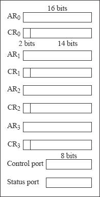
Fig. Programmer's view at a glance of Intel 8257.
We can select any one of the above registers by the address of the four pins marked as A3-0 of 8257. The processor used here writes to AR, CR, control register which sends an appropriate address to the four pins ranging from A3-0 when the chip select and I/O writes at the time when the signals are in active state. Now a short description about the Address Register which contains the address of a memory location that is used in the DMA data transfer scheme. The Address Register, which is used in a DMA transfer scheme, gets automatically incremented by 1 after each and every access to DMA. Since for communicating with the processor, we use only eight pins, the Least Significant and Most Significant bytes of an Address Register can be written in two steps, which starts with the Least Significant byte. First/last flip-flop:8257 has a first/last flip-flop which successively occurs in opposite way of computing after every access of AR or CR. More appropriately this flip-flop is called called as MS/LS* flip-flop. This state of flip-flop decides if MS or LS bytes of an AR/CR are getting into access.
If the M/L* is 0, the Least Significant Byte gets into access;
If M/L* is 1, Most Significant Byte gets into access.

768 Views
