- Power Electronics Tutorial
- Power Electronics - Home
- Power Electronics - Introduction
- Power Electronics - Switching Devices
- Linear Circuit Elements
- Power Semiconductor Devices
- Silicon Controlled Rectifier
- Power Electronics - TRIAC
- Power Electronics - BJT
- Power Electronics - IGBT
- Power Electronics - MOSFET
- Solved Example
- Phase Controlled Converters
- Power Electronics - Pulse Converters
- Effect of Source Inductance
- Performance Parameters
- Reactive Power Control of Converters
- Power Electronics - Dual Converters
- Solved Example
- DC to DC Converters
- Power Electronics - Choppers
- Power Electronics - Control Methods
- Resonant Switching
- DC Converters Solved Example
- AC to DC Converters
- Single Phase AC Voltage Controllers
- Power Electronics - Cycloconverters
- Integral Cycle Control
- Power Electronics - Matrix Converters
- Solved Example
- Power Electronics Resources
- Power Electronics - Quick Guide
- Power Electronics - Useful Resources
- Power Electronics - Discussion
Power Electronics - BJT
A Bipolar Junction Transistor (BJT) is a transistor whose operation depends on the contact made by two semicondutors. It can act as a switch, amplifier or oscillator. It is known as a bipolar transistor since its operation requires two types of charge carriers (holes and electrons). Holes constitute the dominant charge carriers in P-type semiconductors while electrons are the main charge bearers in N-type semiconductors.
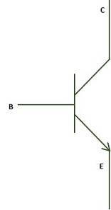
Symbols of a BJT
Structure of a BJT
A BJT has two P-N junctions connected back to back and sharing a common region B (base). This ensures contacts are made in all the regions that are base, collector and emitter. The structure of a PNP bipolar transistor is shown below.
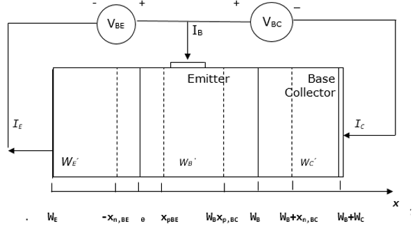
The BJT shown above consists of two diodes connected back to back, resulting in the depletion of the regions called quasi-neutral. The width of quasi-neutral of the emitter, base and collector are indicated above as WE’, WB’ and WC’. They are obtained as follows −
$$W_{E}^{'}=W_{E}-X_{n,BE}$$ $$W_{B}^{'}=W_{B}-X_{p,BE}-X_{p,BC}$$ $$W_{C}^{'}=W_{C}-X_{n,BC}$$The conventional signs of the currents for the emitter, base and collector are denoted by IE, IB and IC respectively. Therefore, the collector and base current are positive when a positive current meets the collector or base contact. In addition, the emitter current is positive when current leaves the emitter contact. Thus,
$$I_{E}=I_{B}+I_{C}$$When a positive voltage is applied to the base contact relative to the collector and emitter, the base-collector voltage as well as base-emitter voltage becomes positive.
For simplicity, VCE is assumed to be zero.
Diffusion of electrons occur from the emitter to the base while diffusion of holes originates from the base to the emitter. Once the electrons reach the base-collector depleted region, they are swept through the region by an electric field. These electrons form the collector current.
When a BJT is biased in the forward active mode, the total emitter current is obtained by adding the electron diffusion current (IE,n), the hole diffusion current (IE, p) and the baseemitter current.
$$I_{E}=I_{E,n}+I_{E,p}+I_{r,d}$$The total collector current is given by the electron diffusion current (IE,n), less the base recombination current(Ir,B).
$$I_{C}=I_{E,n}-I_{r,B}$$The sum of the base current IB is obtained by adding the hole diffusion current (IE, p), base recombination current (Ir,B) and the base-emitter recombination current of the depletion layer (Ir,d).
$$I_{B}=I_{E,p}+I_{r,B}+I_{r,d}$$Transport Factor
This is given by the ratio of the collector current and the emitter current.
$$\alpha =\frac{I_{C}}{I_{E}}$$Applying the Kirchhoff’s current law, it is found that the base current is given by the difference between the emitter current and the collector current.
Current Gain
This is given by the ratio of the collector current to the base current.
$$\beta =\frac{I_{C}}{I_{B}}=\frac{\alpha }{1-\alpha }$$The above explains how a BJT can produce current amplification. The transport factor (α) approaches one if the collector current is almost equivalent to the emitter current. The current gain (β) thus becomes greater than one.
For further analysis, the transport factor (α) is rewritten as a product of the emitter efficiency (γE) the base transport factor (αT) and the recombination factor of the depletion layer (δr). It is rewritten as follows −
$$\alpha =\gamma _{E}\times \alpha _{T}\times \delta _{r}$$The following is a summary of the discussed emitter efficiency, base transport factor and depletion layer recombination factor.