- Home
- Basics of Integrated Circuits Applications
- Basics Operational Amplifier
- Op-Amp applications
- Arithmetic Circuits
- Differentiator & Integrator
- Converters Of Electrical Quantities
- Comparators
- Log & Anti-Log Amplifiers
- Rectifiers
- Clippers
- Clampers
- Active Filters
- Sinusoidal Oscillators
- Waveform Generators
- 555 Timer
- Phase Locked Loop Ic
- Voltage Regulators
- Data Converters
- Digital to Analog Converters
- DAC Example Problem
- Direct Type ADCs
- Indirect Type ADC
Linear Integrated Circuits Applications - Quick Guide
Basics Of Linear Integrated Circuits Applications
An electronic circuit is a group of electronic components connected for a specific purpose.
A simple electronic circuit can be designed easily because it requires few discrete electronic components and connections. However, designing a complex electronic circuit is difficult, as it requires more number of discrete electronic components and their connections. It is also time taking to build such complex circuits and their reliability is also less. These difficulties can be overcome with Integrated Circuits.
Integrated Circuit (IC)
If multiple electronic components are interconnected on a single chip of semiconductor material, then that chip is called as an Integrated Circuit (IC). It consists of both active and passive components.
This chapter discusses the advantages and types of ICs.
Advantages of Integrated Circuits
Integrated circuits offer many advantages. They are discussed below −
Compact size − For a given functionality, you can obtain a circuit of smaller size using ICs, compared to that built using a discrete circuit.
Lesser weight − A circuit built with ICs weighs lesser when compared to the weight of a discrete circuit that is used for implementing the same function of IC. using ICs, compared to that built using a discrete circuit.
Low power consumption − ICs consume lower power than a traditional circuit,because of their smaller size and construction.
Reduced cost − ICs are available at much reduced cost than discrete circuits because of their fabrication technologies and usage of lesser material than discrete circuits.
Increased reliability − Since they employ lesser connections, ICs offer increased reliability compared to digital circuits.
Improved operating speeds − ICs operate at improved speeds because of their switching speeds and lesser power consumption.
Types of Integrated Circuits
Integrated circuits are of two types − Analog Integrated Circuits and Digital Integrated Circuits.
Analog Integrated Circuits
Integrated circuits that operate over an entire range of continuous values of the signal amplitude are called as Analog Integrated Circuits. These are further classified into the two types as discussed here −
Linear Integrated Circuits − An analog IC is said to be Linear, if there exists a linear relation between its voltage and current. IC 741, an 8-pin Dual In-line Package (DIP)op-amp, is an example of Linear IC.
Radio Frequency Integrated Circuits − An analog IC is said to be Non-Linear, if there exists a non-linear relation between its voltage and current. A Non-Linear IC is also called as Radio Frequency IC.
Digital Integrated Circuits
If the integrated circuits operate only at a few pre-defined levels instead of operating for an entire range of continuous values of the signal amplitude, then those are called as Digital Integrated Circuits.
In the coming chapters, we will discuss about various Linear Integrated Circuits and their applications.
Basics Of Operational Amplifier
Operational Amplifier, also called as an Op-Amp, is an integrated circuit, which can be used to perform various linear, non-linear, and mathematical operations. An op-amp is a direct coupled high gain amplifier. You can operate op-amp both with AC and DC signals. This chapter discusses the characteristics and types of op-amps.
Construction of Operational Amplifier
An op-amp consists of differential amplifier(s), a level translator and an output stage. A differential amplifier is present at the input stage of an op-amp and hence an op-amp consists of two input terminals. One of those terminals is called as the inverting terminal and the other one is called as the non-inverting terminal. The terminals are named based on the phase relationship between their respective inputs and outputs.
Characteristics of Operational Amplifier
The important characteristics or parameters of an operational amplifier are as follows −
- Open loop voltage gain
- Output offset voltage
- Common Mode Rejection Ratio
- Slew Rate
This section discusses these characteristics in detail as given below −
Open loop voltage gain
The open loop voltage gain of an op-amp is its differential gain without any feedback path.
Mathematically, the open loop voltage gain of an op-amp is represented as −
$$A_{v}= \frac{v_0}{v_1-v_2}$$
Output offset voltage
The voltage present at the output of an op-amp when its differential input voltage is zero is called as output offset voltage.
Common Mode Rejection Ratio
Common Mode Rejection Ratio (CMRR) of an op-amp is defined as the ratio of the closed loop differential gain, $A_{d}$ and the common mode gain, $A_{c}$.
Mathematically, CMRR can be represented as −
$$CMRR=\frac{A_{d}}{A_{c}}$$
Note that the common mode gain, $A_{c}$ of an op-amp is the ratio of the common mode output voltage and the common mode input voltage.
Slew Rate
Slew rate of an op-amp is defined as the maximum rate of change of the output voltage due to a step input voltage.
Mathematically, slew rate (SR) can be represented as −
$$SR=Maximum\:of\:\frac{\text{d}V_{0}}{\text{d}t}$$
Where, $V_{0}$ is the output voltage. In general, slew rate is measured in either $V/\mu\:Sec$ or $V/m\:Sec$.
Types of Operational Amplifiers
An op-amp is represented with a triangle symbol having two inputs and one output.
Op-amps are of two types: Ideal Op-Amp and Practical Op-Amp.
They are discussed in detail as given below −
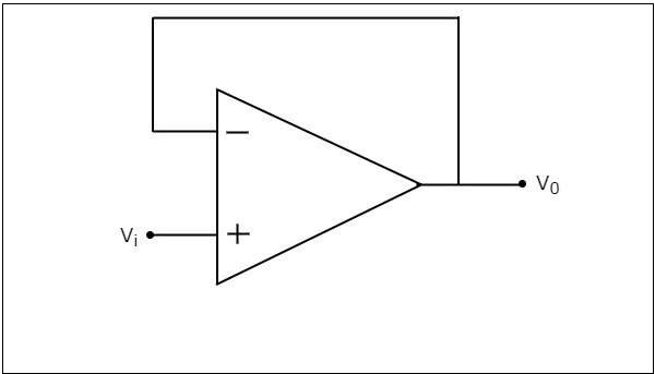
Ideal Op-Amp
An ideal op-amp exists only in theory, and does not exist practically. The equivalent circuit of an ideal op-amp is shown in the figure given below −
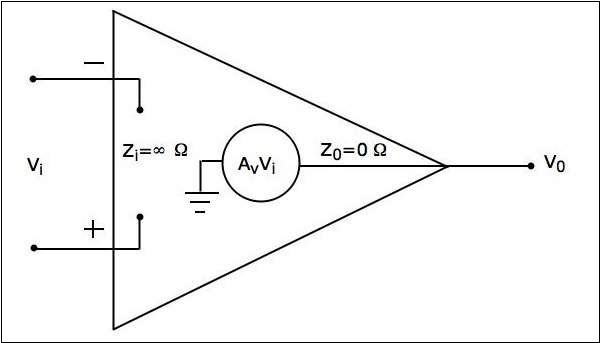
An ideal op-amp exhibits the following characteristics −
Input impedance $Z_{i}=\infty\Omega$
Output impedance $Z_{0}=0\Omega$
Open loop voltage gaine $A_{v}=\infty$
If (the differential) input voltage $V_{i}=0V$, then the output voltage will be $V_{0}=0V$
Bandwidth is infinity. It means, an ideal op-amp will amplify the signals of any frequency without any attenuation.
Common Mode Rejection Ratio (CMRR) is infinity.
Slew Rate (SR) is infinity. It means, the ideal op-amp will produce a change in the output instantly in response to an input step voltage.
Practical Op-Amp
Practically, op-amps are not ideal and deviate from their ideal characteristics because of some imperfections during manufacturing. The equivalent circuit of a practical op-amp is shown in the following figure −
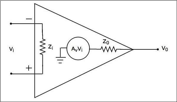
A practical op-amp exhibits the following characteristics −
Input impedance, $Z_{i}$ in the order of Mega ohms.
Output impedance, $Z_{0}$ in the order of few ohms..
Open loop voltage gain, $A_{v}$ will be high.
When you choose a practical op-amp, you should check whether it satisfies the following conditions −
Input impedance, $Z_{i}$ should be as high as possible.
Output impedance, $Z_{0}$ should be as low as possible.
Open loop voltage gain, $A_{v}$ should be as high as possible.
Output offset voltage should be as low as possible.
The operating Bandwidth should be as high as possible.
CMRR should be as high as possible.
Slew rate should be as high as possible.
Note − IC 741 op-amp is the most popular and practical op-amp.
Op-Amp-Applications
A circuit is said to be linear, if there exists a linear relationship between its input and the output. Similarly, a circuit is said to be non-linear, if there exists a non-linear relationship between its input and output.
Op-amps can be used in both linear and non-linear applications. The following are the basic applications of op-amp −
- Inverting Amplifier
- Non-inverting Amplifier
- Voltage follower
This chapter discusses these basic applications in detail.
Inverting Amplifier
An inverting amplifier takes the input through its inverting terminal through a resistor $R_{1}$, and produces its amplified version as the output. This amplifier not only amplifies the input but also inverts it (changes its sign).
The circuit diagram of an inverting amplifier is shown in the following figure −
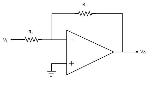
Note that for an op-amp, the voltage at the inverting input terminal is equal to the voltage at its non-inverting input terminal. Physically, there is no short between those two terminals but virtually, they are in short with each other.
In the circuit shown above, the non-inverting input terminal is connected to ground. That means zero volts is applied at the non-inverting input terminal of the op-amp.
According to the virtual short concept, the voltage at the inverting input terminal of an op-amp will be zero volts.
The nodal equation at this terminal's node is as shown below −
$$\frac{0-V_i}{R_1}+ \frac{0-V_0}{R_f}=0$$
$$=>\frac{-V_i}{R_1}= \frac{V_0}{R_f}$$
$$=>V_{0}=\left(\frac{-R_f}{R_1}\right)V_{t}$$
$$=>\frac{V_0}{V_i}= \frac{-R_f}{R_1}$$
The ratio of the output voltage $V_{0}$ and the input voltage $V_{i}$ is the voltage-gain or gain of the amplifier. Therefore, the gain of inverting amplifier is equal to $-\frac{R_f}{R_1}$.
Note that the gain of the inverting amplifier is having a negative sign. It indicates that there exists a 1800 phase difference between the input and the output.
Non-Inverting Amplifier
A non-inverting amplifier takes the input through its non-inverting terminal, and produces its amplified version as the output. As the name suggests, this amplifier just amplifies the input, without inverting or changing the sign of the output.
The circuit diagram of a non-inverting amplifier is shown in the following figure −
In the above circuit, the input voltage $V_{i}$ is directly applied to the non-inverting input terminal of op-amp. So, the voltage at the non-inverting input terminal of the op-amp will be $V_{i}$.
By using voltage division principle, we can calculate the voltage at the inverting input terminal of the op-amp as shown below −
$$=>V_{1} = V_{0}\left(\frac{R_1}{R_1+R_f}\right)$$
According to the virtual short concept, the voltage at the inverting input terminal of an op-amp is same as that of the voltage at its non-inverting input terminal.
$$=>V_{1} = V_{i}$$
$$=>V_{0}\left(\frac{R_1}{R_1+R_f}\right)=V_{i}$$
$$=>\frac{V_0}{V_i}=\frac{R_1+R_f}{R_1}$$
$$=>\frac{V_0}{V_i}=1+\frac{R_f}{R_1}$$
Now, the ratio of output voltage $V_{0}$ and input voltage $V_{i}$ or the voltage-gain or gain of the non-inverting amplifier is equal to $1+\frac{R_f}{R_1}$.
Note that the gain of the non-inverting amplifier is having a positive sign. It indicates that there is no phase difference between the input and the output.
Voltage follower
A voltage follower is an electronic circuit, which produces an output that follows the input voltage. It is a special case of non-inverting amplifier.
If we consider the value of feedback resistor, $R_{f}$ as zero ohms and (or) the value of resistor, 1 as infinity ohms, then a non-inverting amplifier becomes a voltage follower. The circuit diagram of a voltage follower is shown in the following figure −
In the above circuit, the input voltage $V_{i}$ is directly applied to the non-inverting input terminal of the op-amp. So, the voltage at the non-inverting input terminal of op-amp is equal to $V_{i}$. Here, the output is directly connected to the inverting input terminal of opamp. Hence, the voltage at the inverting input terminal of op-amp is equal to $V_{0}$.
According to the virtual short concept, the voltage at the inverting input terminal of the op-amp is same as that of the voltage at its non-inverting input terminal.
$$=>V_{0} = V_{i}$$
So, the output voltage $V_{0}$ of a voltage follower is equal to its input voltage $V_{i}$.
Thus, the gain of a voltage follower is equal to one since, both output voltage $V_{0}$ and input voltage $V_{i}$ of voltage follower are same.
Arithmetic Circuits
In the previous chapter, we discussed about the basic applications of op-amp. Note that they come under the linear operations of an op-amp. In this chapter, let us discuss about arithmetic circuits, which are also linear applications of op-amp.
The electronic circuits, which perform arithmetic operations are called as arithmetic circuits. Using op-amps, you can build basic arithmetic circuits such as an adder and a subtractor. In this chapter, you will learn about each of them in detail.
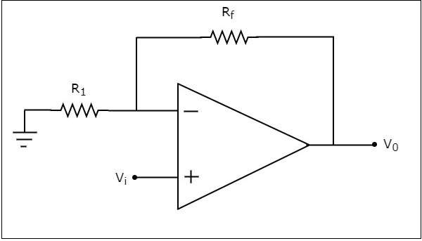
Adder
An adder is an electronic circuit that produces an output, which is equal to the sum of the applied inputs. This section discusses about the op-amp based adder circuit.
An op-amp based adder produces an output equal to the sum of the input voltages applied at its inverting terminal. It is also called as a summing amplifier, since the output is an amplified one.
The circuit diagram of an op-amp based adder is shown in the following figure −
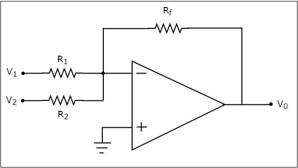
In the above circuit, the non-inverting input terminal of the op-amp is connected to ground. That means zero volts is applied at its non-inverting input terminal.
According to the virtual short concept, the voltage at the inverting input terminal of an op-amp is same as that of the voltage at its non-inverting input terminal. So, the voltage at the inverting input terminal of the op-amp will be zero volts.
The nodal equation at the inverting input terminal's node is
$$\frac{0-V_1}{R_1}+\frac{0-V_2}{R_2}+\frac{0-V_0}{R_f}=0$$
$$=>\frac{V_1}{R_1}-\frac{V_2}{R_2}=\frac{V_0}{R_f}$$
$$=>V_{0}=R_{f}\left(\frac{V_1}{R_1}+\frac{V_2}{R_2}\right)$$
If $R_{f}=R_{1}=R_{2}=R$, then the output voltage $V_{0}$ will be −
$$V_{0}=-R{}\left(\frac{V_1}{R}+\frac{V_2}{R}\right)$$
$$=>V_{0}=-(V_{1}+V_{2})$$
Therefore, the op-amp based adder circuit discussed above will produce the sum of the two input voltages $v_{1}$ and $v_{1}$, as the output, when all the resistors present in the circuit are of same value. Note that the output voltage $V_{0}$ of an adder circuit is having a negative sign, which indicates that there exists a 1800 phase difference between the input and the output.
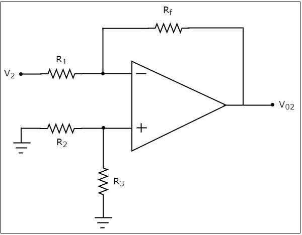
Subtractor
A subtractor is an electronic circuit that produces an output, which is equal to the difference of the applied inputs. This section discusses about the op-amp based subtractor circuit.
An op-amp based subtractor produces an output equal to the difference of the input voltages applied at its inverting and non-inverting terminals. It is also called as a difference amplifier, since the output is an amplified one.
The circuit diagram of an op-amp based subtractor is shown in the following figure −
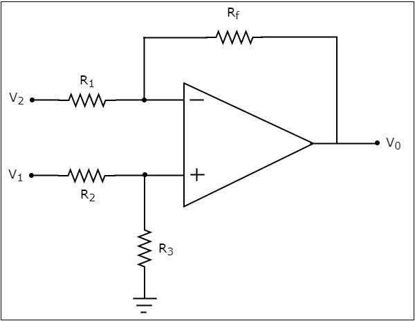
Now, let us find the expression for output voltage $V_{0}$ of the above circuit using superposition theorem using the following steps −
Step 1
Firstly, let us calculate the output voltage $V_{01}$ by considering only $V_{1}$.
For this, eliminate $V_{2}$ by making it short circuit. Then we obtain the modified circuit diagram as shown in the following figure −
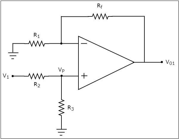
Now, using the voltage division principle, calculate the voltage at the non-inverting input terminal of the op-amp.
$$=>V_{p}=V_{1}\left(\frac{R_3}{R_2+R_3}\right)$$
Now, the above circuit looks like a non-inverting amplifier having input voltage $V_{p}$. Therefore, the output voltage $V_{01}$ of above circuit will be
$$V_{01}=V_{p}\left(1+\frac{R_f}{R_1}\right)$$
Substitute, the value of $V_{p}$ in above equation, we obtain the output voltage $V_{01}$ by considering only $V_{1}$, as −
$$V_{01}=V_{1}\left(\frac{R_3}{R_2+R_3}\right)\left(1+\frac{R_f}{R_1}\right)$$
Step 2
In this step, let us find the output voltage, $V_{02}$ by considering only $V_{2}$. Similar to that in the above step, eliminate $V_{1}$ by making it short circuit. The modified circuit diagram is shown in the following figure.
You can observe that the voltage at the non-inverting input terminal of the op-amp will be zero volts. It means, the above circuit is simply an inverting op-amp. Therefore, the output voltage $V_{02}$ of above circuit will be −
$$V_{02}=\left(-\frac{R_f}{R_1}\right)V_{2}$$
Step 3
In this step, we will obtain the output voltage $V_{0}$ of the subtractor circuit by adding the output voltages obtained in Step1 and Step2. Mathematically, it can be written as
$$V_{0}=V_{01}+V_{02}$$
Substituting the values of $V_{01}$ and $V_{02}$ in the above equation, we get −
$$V_{0}=V_{1}\left(\frac{R_3}{R_2+R_3}\right)\left(1+\frac{R_f}{R_1}\right)+\left(-\frac{R_f}{R_1}\right)V_{2}$$
$$=>V_{0}=V_{1}\left(\frac{R_3}{R_2+R_3}\right)\left(1+\frac{R_f}{R_1}\right)-\left(\frac{R_f}{R_1}\right)V_{2}$$
If $R_{f}=R_{1}=R_{2}=R_{3}=R$, then the output voltage $V_{0}$ will be
$$V_{0}=V_{1}\left(\frac{R}{R+R}\right)\left(1+\frac{R}{R}\right)-\left(\frac{R}{R}\right)V_{2}$$
$$=>V_{0}=V_{1}\left(\frac{R}{2R}\right)(2)-(1)V_{2}$$
$$V_{0}=V_{1}-V_{2}$$
Thus, the op-amp based subtractor circuit discussed above will produce an output, which is the difference of two input voltages $V_{1}$ and $V_{2}$, when all the resistors present in the circuit are of same value.
Differentiator And Integrator
The electronic circuits which perform the mathematical operations such as differentiation and integration are called as differentiator and integrator, respectively.
This chapter discusses in detail about op-amp based differentiator and integrator. Please note that these also come under linear applications of op-amp.
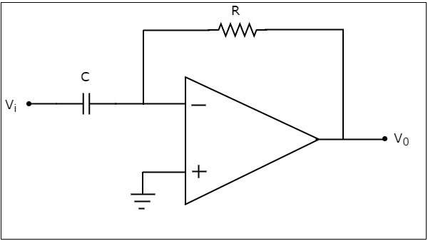
Differentiator
A differentiator is an electronic circuit that produces an output equal to the first derivative of its input. This section discusses about the op-amp based differentiator in detail.
An op-amp based differentiator produces an output, which is equal to the differential of input voltage that is applied to its inverting terminal. The circuit diagram of an op-amp based differentiator is shown in the following figure −
In the above circuit, the non-inverting input terminal of the op-amp is connected to ground. That means zero volts is applied to its non-inverting input terminal.
According to the virtual short concept, the voltage at the inverting input terminal of opamp will be equal to the voltage present at its non-inverting input terminal. So, the voltage at the inverting input terminal of op-amp will be zero volts.
The nodal equation at the inverting input terminal's node is −
$$C\frac{\text{d}(0-V_{i})}{\text{d}t}+\frac{0-V_0}{R}=0$$
$$=>-C\frac{\text{d}V_{i}}{\text{d}t}=\frac{V_0}{R}$$
$$=>V_{0}=-RC\frac{\text{d}V_{i}}{\text{d}t}$$
If $RC=1\sec$, then the output voltage $V_{0}$ will be −
$$V_{0}=-\frac{\text{d}V_{i}}{\text{d}t}$$
Thus, the op-amp based differentiator circuit shown above will produce an output, which is the differential of input voltage $V_{i}$, when the magnitudes of impedances of resistor and capacitor are reciprocal to each other.
Note that the output voltage $V_{0}$ is having a negative sign, which indicates that there exists a 1800 phase difference between the input and the output.
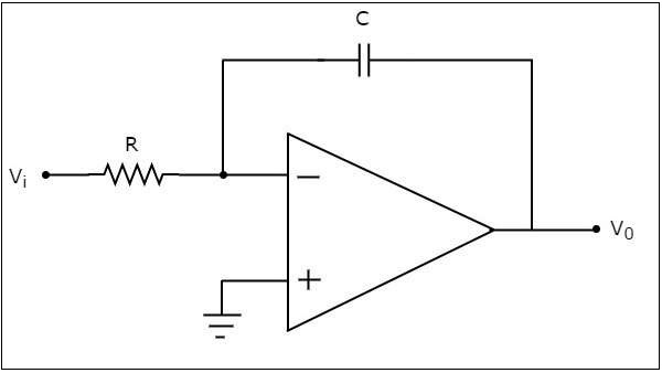
Integrator
An integrator is an electronic circuit that produces an output that is the integration of the applied input. This section discusses about the op-amp based integrator.
An op-amp based integrator produces an output, which is an integral of the input voltage applied to its inverting terminal. The circuit diagram of an op-amp based integrator is shown in the following figure −
In the circuit shown above, the non-inverting input terminal of the op-amp is connected to ground. That means zero volts is applied to its non-inverting input terminal.
According to virtual short concept, the voltage at the inverting input terminal of op-amp will be equal to the voltage present at its non-inverting input terminal. So, the voltage at the inverting input terminal of op-amp will be zero volts.
The nodal equation at the inverting input terminal is −
$$\frac{0-V_i}{R}+C\frac{\text{d}(0-V_{0})}{\text{d}t}=0$$
$$=>\frac{-V_i}{R}=C\frac{\text{d}V_{0}}{\text{d}t}$$
$$=>\frac{\text{d}V_{0}}{\text{d}t}=-\frac{V_i}{RC}$$
$$=>{d}V_{0}=\left(-\frac{V_i}{RC}\right){\text{d}t}$$
Integrating both sides of the equation shown above, we get −
$$\int{d}V_{0}=\int\left(-\frac{V_i}{RC}\right){\text{d}t}$$
$$=>V_{0}=-\frac{1}{RC}\int V_{t}{\text{d}t}$$
If $RC=1\sec$, then the output voltage, $V_{0}$ will be −
$$V_{0}=-\int V_{i}{\text{d}t}$$
So, the op-amp based integrator circuit discussed above will produce an output, which is the integral of input voltage $V_{i}$, when the magnitude of impedances of resistor and capacitor are reciprocal to each other.
Note − The output voltage, $V_{0}$ is having a negative sign, which indicates that there exists 1800 phase difference between the input and the output.
Converters Of Electrical Quantities
Voltage and current are the basic electrical quantities. They can be converted into one another depending on the requirement. Voltage to Current Converter and Current to Voltage Converter are the two circuits that help in such conversion. These are also linear applications of op-amps. This chapter discusses them in detail.
Voltage to Current Converter
A voltage to current converter or V to I converter, is an electronic circuit that takes current as the input and produces voltage as the output. This section discusses about the op-amp based voltage to current converter.
An op-amp based voltage to current converter produces an output current when a voltage is applied to its non-inverting terminal. The circuit diagram of an op-amp based voltage to current converter is shown in the following figure.
In the circuit shown above, an input voltage $V_{i}$ is applied at the non-inverting input terminal of the op-amp. According to the virtual short concept, the voltage at the inverting input terminal of an op-amp will be equal to the voltage at its non-inverting input terminal . So, the voltage at the inverting input terminal of the op-amp will be $V_{i}$.
The nodal equation at the inverting input terminal's node is −
$$\frac{V_i}{R_1}-I_{0}=0$$
$$=>I_{0}=\frac{V_t}{R_1}$$
Thus, the output current $I_{0}$ of a voltage to current converter is the ratio of its input voltage $V_{i}$ and resistance $R_{1}$.
We can re-write the above equation as −
$$\frac{I_0}{V_i}=\frac{1}{R_1}$$
The above equation represents the ratio of the output current $I_{0}$ and the input voltage $V_{i}$ & it is equal to the reciprocal of resistance $R_{1}$ The ratio of the output current $I_{0}$ and the input voltage $V_{i}$ is called as Transconductance.
We know that the ratio of the output and the input of a circuit is called as gain. So, the gain of an voltage to current converter is the Transconductance and it is equal to the reciprocal of resistance $R_{1}$.
Current to Voltage Converter
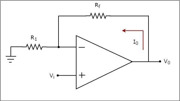
A current to voltage converter or I to V converter is an electronic circuit that takes current as the input and produces voltage as the output. This section discusses about the op-amp based current to voltage converter.
An op-amp based current to voltage converter produces an output voltage when current is applied to its inverting terminal. The circuit diagram of an op-amp based current to voltage converter is shown in the following figure.
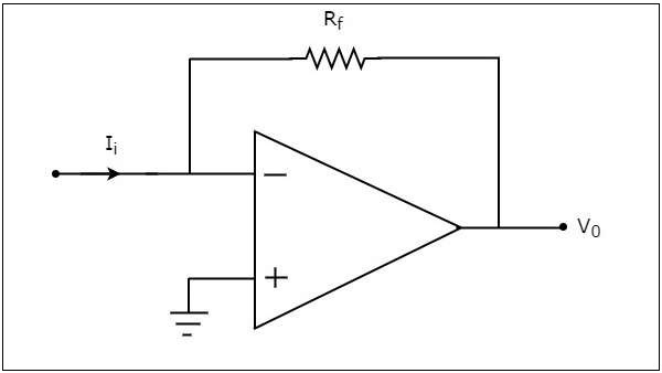
In the circuit shown above, the non-inverting input terminal of the op-amp is connected to ground. That means zero volts is applied at its non-inverting input terminal.
According to the virtual short concept, the voltage at the inverting input terminal of an op-amp will be equal to the voltage at its non-inverting input terminal. So, the voltage at the inverting input terminal of the op-amp will be zero volts.
The nodal equation at the inverting terminal's node is −
$$-I_{i}+\frac{0-V_0}{R_f}=0$$
$$-I_{i}=\frac{V_0}{R_f}$$
$$V_{0}=-R_{t}I_{i}$$
Thus, the output voltage, $V_{0}$ of current to voltage converter is the (negative) product of the feedback resistance, $R_{f}$ and the input current, $I_{t}$. Observe that the output voltage, $V_{0}$ is having a negative sign, which indicates that there exists a 1800 phase difference between the input current and output voltage.
We can re-write the above equation as −
$$\frac{V_0}{I_i}=-R_{f}$$
The above equation represents the ratio of the output voltage $V_{0}$ and the input current $I_{i}$, and it is equal to the negative of feedback resistance, $R_{f}$. The ratio of output voltage $V_{0}$ and input current $I_{i}$ is called as Transresistance.
We know that the ratio of output and input of a circuit is called as gain. So, the gain of a current to voltage converter is its trans resistance and it is equal to the (negative) feedback resistance $R_{f}$ .
Comparators
A comparator is an electronic circuit, which compares the two inputs that are applied to it and produces an output. The output value of the comparator indicates which of the inputs is greater or lesser. Please note that comparator falls under non-linear applications of ICs.
An op-amp consists of two input terminals and hence an op-amp based comparator compares the two inputs that are applied to it and produces the result of comparison as the output. This chapter discusses about op-amp based comparators.
Types of Comparators
Comparators are of two types : Inverting and Non-inverting. This section discusses about these two types in detail.
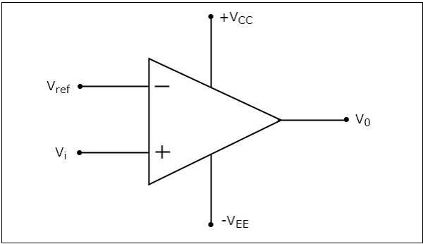
Inverting Comparator
An inverting comparator is an op-amp based comparator for which a reference voltage is applied to its non-inverting terminal and the input voltage is applied to its inverting terminal. This comparator is called as inverting comparator because the input voltage, which has to be compared is applied to the inverting terminal of op-amp.
The circuit diagram of an inverting comparator is shown in the following figure.
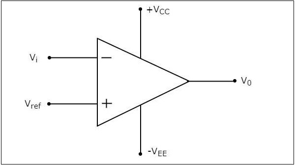
The operation of an inverting comparator is very simple. It produces one of the two values, $+V_{sat}$ and $-V_{sat}$ at the output based on the values of its input voltage $V_{i}$ and the reference voltage $V_{ref}$.
The output value of an inverting comparator will be $-V_{sat}$, for which the input $V_{i}$ voltage is greater than the reference voltage $V_{ref}$.
The output value of an inverting comparator will be $+V_{sat}$, for which the input $V_{i}$ is less than the reference voltage $V_{ref}$.
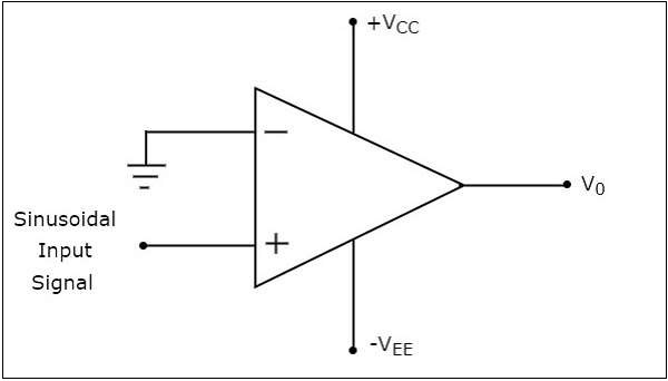
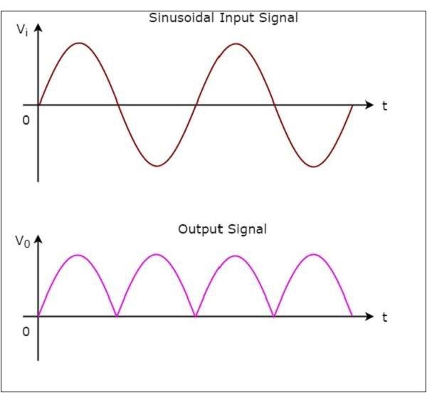
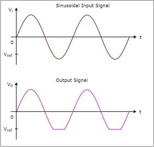
Example
Let us draw the output wave form of an inverting comparator, when a sinusoidal input signal and a reference voltage of zero volts are applied to its inverting and non-inverting terminals respectively.
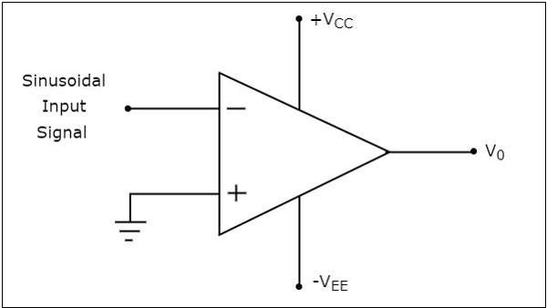
The operation of the inverting comparator shown above is discussed below −
During the positive half cycle of the sinusoidal input signal, the voltage present at the inverting terminal of op-amp is greater than zero volts. Hence, the output value of the inverting comparator will be equal to $-V_{sat}$ during positive half cycle of the sinusoidal input signal.
Similarly, during the negative half cycle of the sinusoidal input signal, the voltage present at the inverting terminal of the op-amp is less than zero volts. Hence, the output value of the inverting comparator will be equal to $+V_{sat}$ during negative half cycle of the sinusoidal input signal.
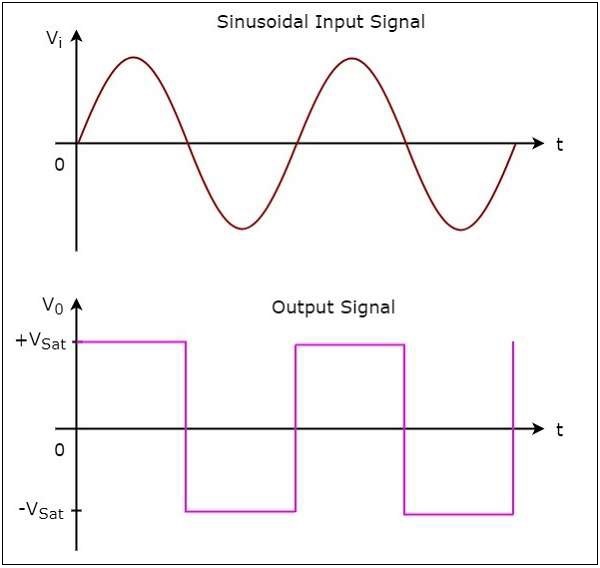
The following figure shows the input and output waveforms of an inverting comparator, when the reference voltage is zero volts.
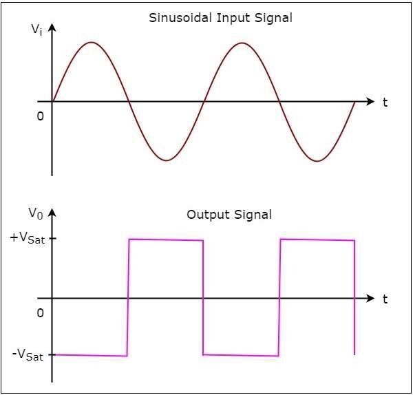
In the figure shown above, we can observe that the output transitions either from $-V_{sat}$ to $+V_{sat}$ or from $+V_{sat}$ to $-V_{sat}$ whenever the sinusoidal input signal is crossing zero volts. In other words, output changes its value when the input is crossing zero volts. Hence, the above circuit is also called as inverting zero crossing detector.
Non-Inverting Comparator
A non-inverting comparator is an op-amp based comparator for which a reference voltage is applied to its inverting terminal and the input voltage is applied to its non-inverting terminal. This op-amp based comparator is called as non-inverting comparator because the input voltage, which has to be compared is applied to the non-inverting terminal of the op-amp.
The circuit diagram of a non-inverting comparator is shown in the following figure
The operation of a non-inverting comparator is very simple. It produces one of the two values, $+V_{sat}$ and $-V_{sat}$ at the output based on the values of input voltage $V_{t}$ and the reference voltage $+V_{ref}$.
The output value of a non-inverting comparator will be $+V_{sat}$, for which the input voltage $V_{i}$ is greater than the reference voltage $+V_{ref}$.
The output value of a non-inverting comparator will bee $-V_{sat}$, for which the input voltage $V_{i}$ is less than the reference voltage $+V_{ref}$.
Example
Let us draw the output wave form of a non-inverting comparator, when a sinusoidal input signal and reference voltage of zero volts are applied to the non-inverting and inverting terminals of the op-amp respectively.
The operation of a non-inverting comparator is explained below −
During the positive half cycle of the sinusoidal input signal, the voltage present at the non-inverting terminal of op-amp is greater than zero volts. Hence, the output value of a non-inverting comparator will be equal to $+V_{sat}$ during the positive half cycle of the sinusoidal input signal.
Similarly, during the negative half cycle of the sinusoidal input signal, the voltage present at the non-inverting terminal of op-amp is less than zero volts. Hence, the output value of non-inverting comparator will be equal to $-V_{sat}$ during the negative half cycle of the sinusoidal input signal.
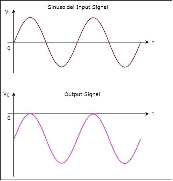
The following figure shows the input and output waveforms of a non-inverting comparator, when the reference voltage is zero volts.
From the figure shown above, we can observe that the output transitions either from $+V_{sat}$ to $-V_{sat}$ or from $-V_{sat}$ to $+V_{sat}$ whenever the sinusoidal input signal crosses zero volts. That means, the output changes its value when the input is crossing zero volts. Hence, the above circuit is also called as non-inverting zero crossing detector.
Log And Anti Log Amplifiers
The electronic circuits which perform the mathematical operations such as logarithm and anti-logarithm (exponential) with an amplification are called as Logarithmic amplifier and Anti-Logarithmic amplifier respectively.
This chapter discusses about the Logarithmic amplifier and Anti-Logarithmic amplifier in detail. Please note that these amplifiers fall under non-linear applications.
Logarithmic Amplifier
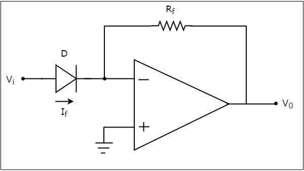
A logarithmic amplifier, or a log amplifier, is an electronic circuit that produces an output that is proportional to the logarithm of the applied input. This section discusses about the op-amp based logarithmic amplifier in detail.
An op-amp based logarithmic amplifier produces a voltage at the output, which is proportional to the logarithm of the voltage applied to the resistor connected to its inverting terminal. The circuit diagram of an op-amp based logarithmic amplifier is shown in the following figure −
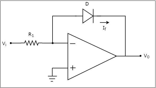
In the above circuit, the non-inverting input terminal of the op-amp is connected to ground. That means zero volts is applied at the non-inverting input terminal of the op-amp.
According to the virtual short concept, the voltage at the inverting input terminal of an op-amp will be equal to the voltage at its non-inverting input terminal. So, the voltage at the inverting input terminal will be zero volts.
The nodal equation at the inverting input terminals node is −
$$\frac{0-V_i}{R_1}+I_{f}=0$$
$$=>I_{f}=\frac{V_i}{R_1}......Equation 1$$
The following is the equation for current flowing through a diode, when it is in forward bias −
$$I_{f}=I_{s} e^{(\frac{V_f}{nV_T})} ......Equation 2$$
where,
$I_{s}$ is the saturation current of the diode,
$V_{f}$ is the voltage drop across diode, when it is in forward bias,
$V_{T}$ is the diodes thermal equivalent voltage.
The KVL equation around the feedback loop of the op amp will be −
$$0-V_{f}-V_{0}=0$$
$$=>V_{f}=-V_{0}$$
Substituting the value of $V_{f}$ in Equation 2, we get −
$$I_{f}=I_{s} e^{\left(\frac{-V_0}{nV_T}\right)} ......Equation 3$$
Observe that the left hand side terms of both equation 1 and equation 3 are same. Hence, equate the right hand side term of those two equations as shown below −
$$\frac{V_i}{R_1}=I_{s}e^{\left(\frac{-V_0}{nV_T}\right)}$$
$$\frac{V_i}{R_1I_s}= e^{\left(\frac{-V_0}{nV_T}\right)}$$
Applying natural logarithm on both sides, we get −
$$In\left(\frac{V_i}{R_1I_s}\right)= \frac{-V_0}{nV_T}$$
$$V_{0}=-{nV_T}In\left(\frac{V_i}{R_1I_s}\right)$$
Note that in the above equation, the parameters n, ${V_T}$ and $I_{s}$ are constants. So, the output voltage $V_{0}$ will be proportional to the natural logarithm of the input voltage $V_{i}$ for a fixed value of resistance $R_{1}$.
Therefore, the op-amp based logarithmic amplifier circuit discussed above will produce an output, which is proportional to the natural logarithm of the input voltage ${V_T}$, when ${R_1I_s}=1V$.
Observe that the output voltage $V_{0}$ has a negative sign, which indicates that there exists a 1800 phase difference between the input and the output.
Anti-Logarithmic Amplifier
An anti-logarithmic amplifier, or an anti-log amplifier, is an electronic circuit that produces an output that is proportional to the anti-logarithm of the applied input. This section discusses about the op-amp based anti-logarithmic amplifier in detail.
An op-amp based anti-logarithmic amplifier produces a voltage at the output, which is proportional to the anti-logarithm of the voltage that is applied to the diode connected to its inverting terminal.
The circuit diagram of an op-amp based anti-logarithmic amplifier is shown in the following figure −
In the circuit shown above, the non-inverting input terminal of the op-amp is connected to ground. It means zero volts is applied to its non-inverting input terminal.
According to the virtual short concept, the voltage at the inverting input terminal of op-amp will be equal to the voltage present at its non-inverting input terminal. So, the voltage at its inverting input terminal will be zero volts.
The nodal equation at the inverting input terminals node is −
$$-I_{f}+\frac{0-V_0}{R_f}=0$$
$$=>-\frac{V_0}{R_f}=I_{f}$$
$$=>V_{0}=-R_{f}I_{f}.........Equation 4$$
We know that the equation for the current flowing through a diode, when it is in forward bias, is as given below −
$$I_{f}=I_{s} e^{\left(\frac{V_f}{nV_T}\right)}$$
Substituting the value of $I_{f}$ in Equation 4, we get
$$V_{0}=-R_{f}\left \{{I_{s} e^{\left(\frac{V_f}{nV_T}\right)}}\right \}$$
$$V_{0}=-R_{f}{I_{s} e^{\left(\frac{V_f}{nV_T}\right)}}......Equation 5$$
The KVL equation at the input side of the inverting terminal of the op amp will be
$$V_{i}-V_{f}=0$$
$$V_{f}=V_{i}$$
Substituting, the value of in the Equation 5, we get −
$$V_{0}=-R_{f}{I_{s} e^{\left(\frac{V_i}{nV_T}\right)}}$$
Note that, in the above equation the parameters n, ${V_T}$ and $I_{s}$ are constants. So, the output voltage ${V_0}$ will be proportional to the anti-natural logarithm (exponential) of the input voltage ${V_i}$, for a fixed value of feedback resistance ${R_f}$.
Therefore, the op-amp based anti-logarithmic amplifier circuit discussed above will produce an output, which is proportional to the anti-natural logarithm (exponential) of the input voltage ${V_i}$ when, ${R_fI_s}= 1V$. Observe that the output voltage ${V_0}$ is having a negative sign, which indicates that there exists a 1800 phase difference between the input and the output.
Rectifiers
AC and DC are two frequent terms that you encounter while studying the flow of electrical charge. Alternating Current (AC) has the property to change its state continuously. For example, if we consider a sine wave, the current flows in one direction for positive half cycle and in the opposite direction for negative half cycle. On the other hand, Direct Current (DC) flows only in one direction.
An electronic circuit, which produces either DC signal or a pulsated DC signal, when an AC signal is applied to it is called as a rectifier. This chapter discusses about op-amp based rectifiers in detail.
Types of Rectifiers
Rectifiers are classified into two types: Half wave rectifier and Full wave rectifier. This section discusses about these two types in detail.
Half wave Rectifier
A half wave rectifier is a rectifier that produces positive half cycles at the output for one half cycle of the input and zero output for the other half cycle of the input.
The circuit diagram of a half wave rectifier is shown in the following figure.
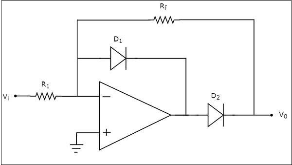
Observe that the circuit diagram of a half wave rectifier shown above looks like an inverting amplifier, with two diodes D1 and D2 in addition.
The working of the half wave rectifier circuit shown above is explained below
For the positive half cycle of the sinusoidal input, the output of the op-amp will be negative. Hence, diode D1 will be forward biased.
When diode D1 is in forward bias, output voltage of the op-amp will be -0.7 V. So, diode D2 will be reverse biased. Hence, the output voltage of the above circuit is zero volts.
Therefore, there is no (zero) output of half wave rectifier for the positive half cycle of a sinusoidal input.
For the negative half cycle of sinusoidal input, the output of the op-amp will be positive. Hence, the diodes D1 and D2 will be reverse biased and forward biased respectively. So, the output voltage of above circuit will be −
$$V_0=-\left(\frac{R_f}{R_1}\right)V_1$$
Therefore, the output of a half wave rectifier will be a positive half cycle for a negative half cycle of the sinusoidal input.
Wave forms
The input and output waveforms of a half wave rectifier are shown in the following figure
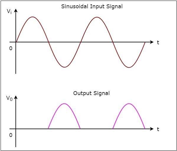
As you can see from the above graph, the half wave rectifier circuit diagram that we discussed will produce positive half cycles for negative half cycles of sinusoidal input and zero output for positive half cycles of sinusoidal input
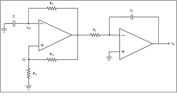
Full wave Rectifier
A full wave rectifier produces positive half cycles at the output for both half cycles of the input.
The circuit diagram of a full wave rectifier is shown in the following figure −
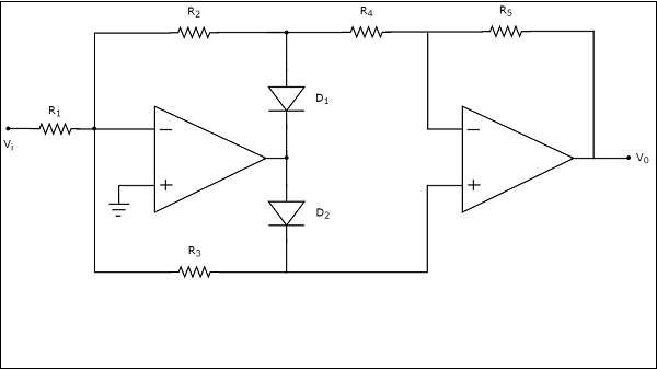
The above circuit diagram consists of two op-amps, two diodes, D1 & D2 and five resistors, R1 to R5. The working of the full wave rectifier circuit shown above is explained below −
For the positive half cycle of a sinusoidal input, the output of the first op-amp will be negative. Hence, diodes D1 and D2 will be forward biased and reverse biased respectively.
Then, the output voltage of the first op-amp will be −
$$V_{01}=-\left(\frac{R_2}{R_1}\right)V_i$$
Observe that the output of the first op-amp is connected to a resistor R4, which is connected to the inverting terminal of the second op-amp. The voltage present at the non-inverting terminal of second op-amp is 0 V. So, the second op-amp with resistors, R4 and R4 acts as an inverting amplifier.
The output voltage of the second op-amp will be
$$V_0=-\left(\frac{R_5}{R_4}\right)V_{01}$$
Substituting the value of $V_{01}$ in the above equation, we get −
$$=>V_{0}=-\left(\frac{R_5}{R_4}\right)\left \{ -\left(\frac{R_2}{R_1}\right)V_{i} \right \}$$
$$=>V_{0}=\left(\frac{R_2R_5}{R_1R_4}\right)V_{i}$$
Therefore, the output of a full wave rectifier will be a positive half cycle for the positive half cycle of a sinusoidal input. In this case, the gain of the output is $\frac{R_2R_5}{R_1R_4}$. If we consider $R_{1}=R_{2}=R_{4}=R_{5}=R$, then the gain of the output will be one.
For the negative half cycle of a sinusoidal input, the output of the first op-amp will be positive. Hence, diodes D1 and D2 will be reverse biased and forward biased respectively.
The output voltage of the first op-amp will be −
$$V_{01}=-\left(\frac{R_3}{R_1}\right)V_{i}$$
The output of the first op-amp is directly connected to the non-inverting terminal of the second op-amp. Now, the second op-amp with resistors, R4 and R5 acts as a non-inverting amplifier.
The output voltage of the second op-amp will be −
$$V_{0}=\left(1+\frac{R_5}{R_4}\right)V_{01}$$
Substituting the value of $V_{01}$ in the above equation, we get
$$=>V_{0}=\left(1+\frac{R_5}{R_4}\right) \left\{-\left(\frac{R_3}{R_1}\right)V_{i}\right \} $$
$$=>V_{0}=-\left(\frac{R_3}{R_1}\right)\left(1+\frac{R_5}{R_4}\right)V_{i}$$
Therefore, the output of a full wave rectifier will be a positive half cycle for the negative half cycle of sinusoidal input also. In this case, the magnitude of the gain of the output is $\left(\frac{R_3}{R_1}\right)\left(1+\frac{R_5}{R_4}\right)$. If we consider $R_{1}=2R_{3}=R_{4}=R_{5}=R$ then the gain of the output will be one.
The input and output waveforms of a full wave rectifier are shown in the following figure
As you can see in the above figure, the full wave rectifier circuit diagram that we considered will produce only positive half cycles for both positive and negative half cycles of a sinusoidal input.
Clippers
Wave shaping circuits are the electronic circuits, which produce the desired shape at the output from the applied input wave form. These circuits perform two functions −
- Attenuate the applied wave
- Alter the dc level of the applied wave.
There are two types of wave shaping circuits: Clippers and Clampers. In this chapter, you will learn in detail about clippers.
Op-amp based Clippers
A clipper is an electronic circuit that produces an output by removing a part of the input above or below a reference value. That means, the output of a clipper will be same as that of the input for other than the clipped part. Due to this, the peak to peak amplitude of the output of a clipper will be always less than that of the input.
The main advantage of clippers is that they eliminate the unwanted noise present in the amplitude of an ac signal.
Clippers can be classified into the following two types based on the clipping portion of the input.
- Positive Clipper
- Negative Clipper
These are discussed in detail as given below −
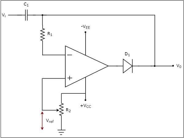
Positive Clipper
A positive clipper is a clipper that clips only the positive portion(s) of the input signal.
The circuit diagramof positive clipper is shown in the following figure −
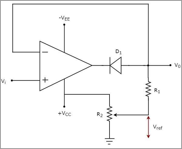
In the circuit shown above, a sinusoidal voltage signal $V_{t}$ is applied to the non-inverting terminal of the op-amp. The value of the reference voltage $V_{ref}$ can be chosen by varying the resistor $R_{2}$.
The operation of the circuit shown above is explained below −
If the value of the input voltage $V_i$ is less than the value of the reference voltage $V_{ref}$, then the diode D1 conducts. Then, the circuit given above behaves as a voltage follower. Therefore, the output voltage $V_{0}$ of the above circuit will be same as that of the input voltage $V_{i}$, for $V_{i}$ < $V_{ref}$.
If the value of the input voltage $V_{i}$ is greater than the value of reference voltage $V_{ref}$, then the diode D1 will be off. Now, the op-amp operates in an open loop since the feedback path was open. Therefore, the output voltage $V_{0}$ of the above circuit will be equal to the value of the reference voltage $V_{ref}$, for $V_{i}$ > $V_{ref}$.
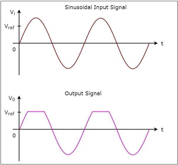
The input wave form and the corresponding output wave form of a positive clipper for a positive reference voltage $V_{ref}$, are shown in the following figure −
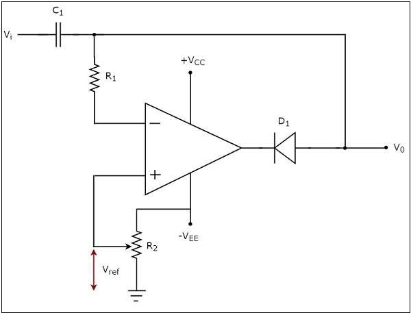
Negative Clipper
A negative clipper is a clipper that clips only the negative portion(s) of the input signal. You can obtain the circuit of the negative clipper just by reversing the diode and taking the reverse polarity of the reference voltage, in the circuit that you have seen for a positive clipper.
The circuit diagram of a negative clipper is shown in the following figure −
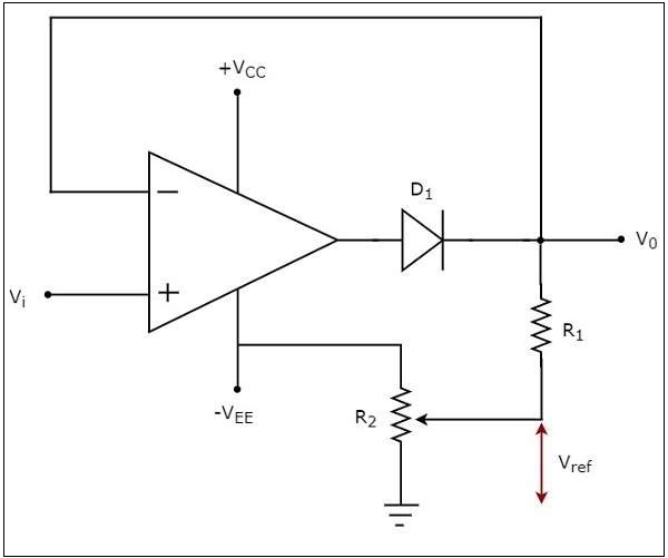
In the above circuit, a sinusoidal voltage signal $V_{i}$ is applied to the non-inverting terminal of the op-amp. The value of the reference voltage $V_{ref}$ can be chosen by varying the resistor $R_{2}$.
The operation of a negative clipper circuit is explained below −
If the value of the input voltage $V_{t}$ is greater than the value of reference voltage $V_{ref}$, then the diode D1 conducts. Then, the above circuit behaves as a voltage follower. Therefore, the output voltage $V_{0}$ of the above circuit will be same as that of the input voltage $V_{i}$ for $V_{i}$> $V_{ref}$.
If the value of the input voltage $V_{i}$ is less than the value of reference voltage , then the diode D1 will be off. Now, the op-amp operates in an open loop since the feedback path is open. Therefore, the output voltage $V_{0}$ of the above circuit will be equal to the value of reference voltage ,$V_{ref}$ for $V_{i}$ < $V_{ref}$.
The input wave form and the corresponding output wave form of a negative clipper, for a negative reference voltage $V_{ref}$, are shown in the following figure −
Clampers
In the previous chapter, we discussed about clippers. Now, let us discuss about other type of wave shaping circuits, namely clampers.
Op-amp based Clampers
A clamper is an electronic circuit that produces an output, which is similar to the input but with a shift in the DC level. In other words, the output of a clamper is an exact replica of the input. Hence, the peak to peak amplitude of the output of a clamper will be always equal to that of the input.
Clampers are used to introduce or restore the DC level of input signal at the output. There are two types of op-amp based clampers based on the DC shift of the input.
- Positive Clamper
- Negative Clamper
This section discusses about these two types of clampers in detail.
Positive Clamper
A positive clamper is a clamper circuit that produces an output in such a way that the input signal gets shifted vertically by a positive DC value.
The circuit diagram of a positive clamper is shown in the following figure −
In the above circuit, a sinusoidal voltage signal, $V_{i}$ is applied to the inverting terminal of op-amp through a network that consists of a capacitor $C_{1}$ and a resistor $R_{1}$. That means, AC voltage signal is applied to the inverting terminal of the op-amp.
The DC reference voltage $V_{ref}$ is applied to the non-inverting terminal of the op-amp. The value of reference voltage $V_{ref}$ can be chosen by varying the resistor $R_{2}$. In this case, we will get a reference voltage $V_{ref}$ of a positive value.
The above circuit produces an output, which is the combination (resultant sum) of the sinusoidal voltage signal $V_{i}$ and the reference voltage $V_{ref}$. That means, the clamper circuit produces an output in such a way that the sinusoidal voltage signal $V_{i}$ gets shifted vertically upwards by the value of reference voltage $V_{ref}$.
The input wave form and the corresponding output wave form of positive clamper are shown in above figure −
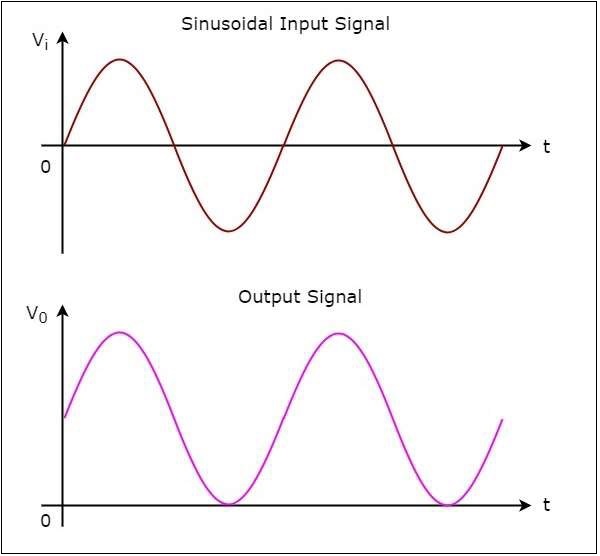
From the figure above, you can observe that the positive clamper shifts the applied input waveform vertically upward at the output. The amount of shift will depend on the value of the DC reference voltage.
Negative Clamper
A negative clamper is a clamper circuit that produces an output in such a way that the input signal gets shifted vertically by a negative DC value.
The circuit diagram of negative clamper is shown in the following figure −
In the above circuit, a sinusoidal voltage signal $V_{i}$ is applied to the inverting terminal of the op-amp through a network that consists of a capacitor C1 and resistor $R_{1}$. That means, AC voltage signal is applied to the inverting terminal of the op-amp.
The DC reference voltage $V_{ref}$ is applied to the non-inverting terminal of the op-amp.The value of reference voltage $V_{ref}$ can be chosen by varying the resistor $R_{2}$. In this case,we will get reference voltage $V_{ref}$ of a negative value.
The above circuit produces an output, which is the combination (resultant sum) of sinusoidal voltage signal $V_{i}$ and reference voltage $V_{ref}$. That means, the clamper circuit produces an output in such a way that the sinusoidal voltage signal $V_{i}$ gets shifted vertically downwards by the value of reference voltage $V_{ref}$.
The input wave form and the corresponding output wave form of a negative clamper are shown in the following figure −
We can observe from the output that the negative clamper shifts the applied input waveform vertically downward at the output. The amount of shifting will depend on the value of DC reference voltage.
Active Filters
Filters are electronic circuits that allow certain frequency components and / or reject some other. You might have come across filters in network theory tutorial. They are passive and are the electric circuits or networks that consist of passive elements like resistor, capacitor, and (or) an inductor.
This chapter discusses about active filters in detail.
Types of Active Filters
Active filters are the electronic circuits, which consist of active element like op-amp(s) along with passive elements like resistor(s) and capacitor(s).
Active filters are mainly classified into the following four types based on the band of frequencies that they are allowing and / or rejecting −
- Active Low Pass Filter
- Active High Pass Filter
- Active Band Pass Filter
- Active Band Stop Filter
Active Low Pass Filter
If an active filter allows (passes) only low frequency components and rejects (blocks) all other high frequency components, then it is called as an active low pass filter.
The circuit diagram of an active low pass filter is shown in the following figure −
We know that the electric network, which is connected to the non-inverting terminal of an op-amp is a passive low pass filter. So, the input of a non-inverting terminal of an opamp is the output of a passive low pass filter.
Observe that the above circuit resembles a non-inverting amplifier. It is having the output of a passive low pass filter as an input to the non-inverting terminal of op-amp. Hence, it produces an output, which is $\left(1+\frac{R_f}{R_1}\right)$ times the input present at the non-inverting terminal.
We can choose the values of $R_{f}$ and $R_{1}$ suitably in order to obtain the desired gain at the output. Suppose, if we consider the resistance values of $R_{f}$ and $R_{1}$ as zero ohms and infinity ohms, then the above circuit will produce a unity gain low pass filter output.
Active High Pass Filter
If an active filter allows (passes) only high frequency components and rejects (blocks) all other low frequency components, then it is called an active high pass filter.
The circuit diagram of an active high pass filter is shown in the following figure −
We know that the electric network, which is connected to the non-inverting terminal of an op-amp is a passive high pass filter. So, the input of a non-inverting terminal of opamp is the output of passive high pass filter.
Now, the above circuit resembles a non-inverting amplifier. It is having the output of a passive high pass filter as an input to non-inverting terminal of op-amp. Hence, it produces an output, which is $\left(1+\frac{R_f}{R_1}\right)$ times the input present at its non-inverting terminal.
We can choose the values of $R_f$ and $R_1$ suitably in order to obtain the desired gain at the output. Suppose, if we consider the resistance values of $R_{f}$ and $R_{1}$ as zero ohms and infinity ohms, then the above circuit will produce a unity gain high pass filter output.
Active Band Pass Filter
If an active filter allows (passes) only one band of frequencies, then it is called as an active band pass filter. In general, this frequency band lies between low frequency range and high frequency range. So, active band pass filter rejects (blocks) both low and high frequency components.
The circuit diagram of an active band pass filter is shown in the following figure
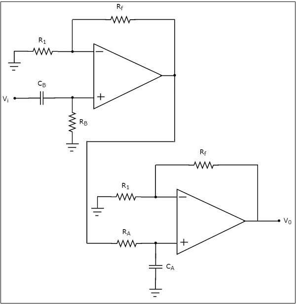
Observe that there are two parts in the circuit diagram of active band pass filter: The first part is an active high pass filter, while the second part is an active low pass filter.
The output of the active high pass filter is applied as an input of the active low pass filter.That means, both active high pass filter and active low pass filter are cascaded in order to obtain the output in such a way that it contains only a particular band of frequencies.
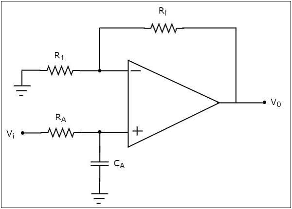
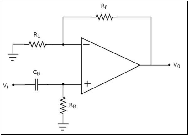
The active high pass filter, which is present at the first stage allows the frequencies that are greater than the lower cut-off frequency of the active band pass filter. So, we have to choose the values of $R_{B}$ and $C_{B}$ suitably, to obtain the desired lower cut-off frequency of the active band pass filter.
Similarly, the active low pass filter, which is present at the second stage allows the frequencies that are smaller than the higher cut-off frequency of the active band pass filter. So, we have to choose the values of $R_{A}$ and $C_{A}$ suitably in order to obtain the desired higher cut-off frequency of the active band pass filter.
Hence, the circuit in the diagram discussed above will produce an active band pass filter output.
Active Band Stop Filter
If an active filter rejects (blocks) a particular band of frequencies, then it is called as an active band stop filter. In general, this frequency band lies between low frequency range and high frequency range. So, active band stop filter allows (passes) both low and high frequency components.
The block diagram of an active band stop filter is shown in the following figure −
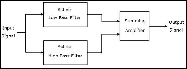
Observe that the block diagram of an active band stop filter consists of two blocks in its first stage: an active low pass filter and an active high pass filter. The outputs of these two blocks are applied as inputs to the block that is present in the second stage. So, the summing amplifier produces an output, which is the amplified version of sum of the outputs of the active low pass filter and the active high pass filter.
Therefore, the output of the above block diagram will be the output of an active band stop , when we choose the cut-off frequency of low pass filter to be smaller than cut-off frequency of a high pass filter.
The circuit diagram of an active band stop filter is shown in the following figure −
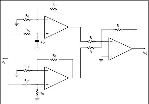
We have already seen the circuit diagrams of an active low pass filter, an active high pass filter and a summing amplifier. Observe that we got the above circuit diagram of active band stop filter by replacing the blocks with the respective circuit diagrams in the block diagram of an active band stop filter.
Sinusoidal Oscillators
An oscillator is an electronic circuit that produces a periodic signal. If the oscillator produces sinusoidal oscillations, it is called as a sinusoidal oscillator. It converts the input energy from a DC source into an AC output energy of a periodic signal. This periodic signal will be having a specific frequency and amplitude.
The block diagram of a sinusoidal oscillator is shown in the following figure −
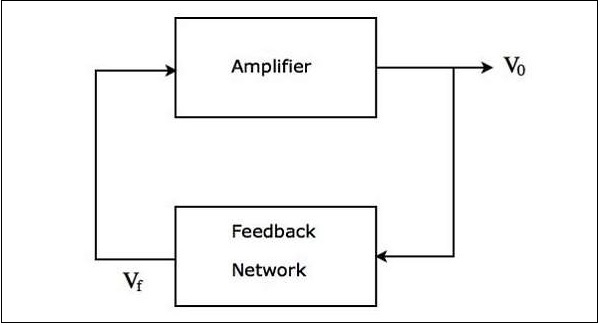
The above figure mainly consists of two blocks: an amplifier and a feedback network.The feedback network takes a part of the output of amplifier as an input to it and produces a voltage signal. This voltage signal is applied as an input to the amplifier.
The block diagram of a sinusoidal oscillator shown above produces sinusoidal oscillations, when the following two conditions are satisfied −
The loop gain $A_{v}\beta$ of the above block diagram of sinusoidal oscillator must be greater than or equal to unity. Here, $A_{v}$ and $\beta$ are the gain of amplifier and gain of the feedback network, respectively.
The total phase shift around the loop of the above block diagram of a sinusoidal oscillator must be either 00 or 3600.
The above two conditions together are called as Barkhausen criteria.
Op-Amp Based Oscillators
There are two types of op-amp based oscillators.
- RC phase shift oscillator
- Wien bridge oscillator
This section discusses each of them in detail.
RC Phase Shift Oscillator
The op-amp based oscillator, which produces a sinusoidal voltage signal at the output with the help of an inverting amplifier and a feedback network is known as a RC phase shift oscillator. This feedback network consists of three cascaded RC sections.
The circuit diagram of a RC phase shift oscillator is shown in the following figure −
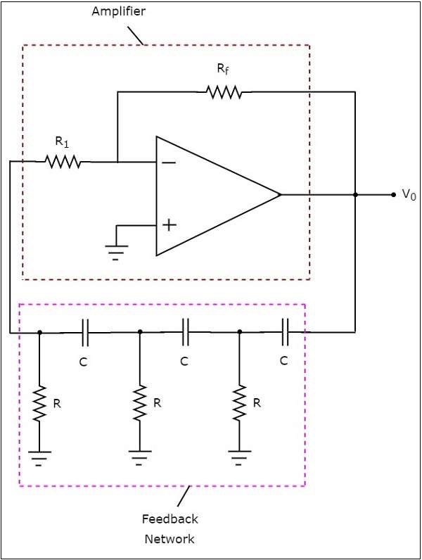
In the above circuit, the op-amp is operating in inverting mode. Hence, it provides a phase shift of 1800. The feedback network present in the above circuit also provides a phase shift of 1800, since each RC section provides a phase shift of 600. Therefore, the above circuit provides a total phase shift of 3600 at some frequency.
The output frequency of a RC phase shift oscillator is −
$$f=\frac{1}{2\Pi RC\sqrt[]{6}}$$
The gain $A_{v}$ of an inverting amplifier should be greater than or equal to -29,
$$i.e.,-\frac{R_f}{R_1}\geq-29$$
$$=>\frac{R_f}{R_1}\geq-29$$
$$=>R_{f}\geq29R_{1}$$
So, we should consider the value of feedback resistor $R_{f}$, as minimum of 29 times the value of resistor $R_{1}$, in order to produce sustained oscillations at the output of a RC phase shift oscillator.
Wien Bridge Oscillator
The op-amp based oscillator, which produces a sinusoidal voltage signal at the output with the help of a non-inverting amplifier and a feedback network is known as Wien bridge oscillator.
The circuit diagram of a Wien bridge oscillator is shown in the following figure −
In the circuit shown above for Wein bridge oscillator, the op-amp is operating in non inverting mode. Hence, it provides a phase shift of 00. So, the feedback network present in the above circuit should not provide any phase shift.
If the feedback network provides some phase shift, then we have to balance the bridge in such a way that there should not be any phase shift. So, the above circuit provides a total phase shift of 00 at some frequency.
The output frequency of Wien bridge oscillator is
$$f=\frac{1}{2\Pi RC}$$
The gain $A_{v}$ of the non-inverting amplifier should be greater than or equal to 3
$$i.e.,1+\frac{R_f}{R_1}\geq3$$
$$=>\frac{R_f}{R_1}\geq2$$
$$=>R_{f}\geq2R_{1}$$
So, we should consider the value of feedback resistor $R_{f}$ at least twice the value of resistor, $R_{1}$ in order to produce sustained oscillations at the output of Wien bridge oscillator.
Waveform Generators
A waveform generator is an electronic circuit, which generates a standard wave. There are two types of op-amp based waveform generators −
- Square wave generator
- Triangular wave generator
This chapter discusses each of these op-amp based waveform generators in detail.
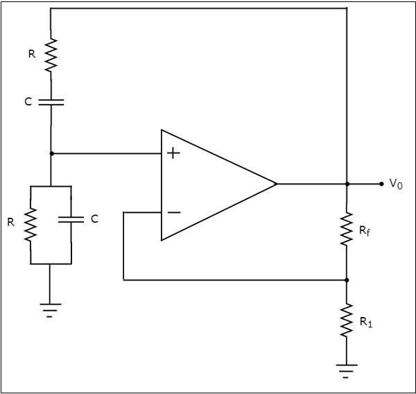
Square Wave Generator
A square wave generator is an electronic circuit which generates square wave. This section discusses about op-amp based square wave generators.
The circuit diagram of a op-amp based square wave generator is shown in the following figure
Observe that in the circuit diagram shown above, the resistor $R_{1}$ is connected between the inverting input terminal of the op-amp and its output of op-amp. So, the resistor $R_{1}$ is used in the negative feedback. Similarly, the resistor $R_{2}$ is connected between the noninverting input terminal of the op-amp and its output. So, the resistor $R_{2}$ is used in the positive feedback path.
A capacitor C is connected between the inverting input terminal of the op-amp and ground. So, the voltage across capacitor C will be the input voltage at this inverting terminal of op-amp. Similarly, a resistor $R_{3}$ is connected between the non-inverting input terminal of the op-amp and ground. So, the voltage across resistor $R_{3}$ will be the input voltage at this non-inverting terminal of the op-amp.
The operation of a square wave generator is explained below −
Assume, there is no charge stored in the capacitor initially. Then, the voltage present at the inverting terminal of the op-amp is zero volts. But, there is some offset voltage at non-inverting terminal of op-amp. Due to this, the value present at the output of above circuit will be $+V_{sat}$.
Now, the capacitor C starts charging through a resistor $R_{1}$. The value present at the output of the above circuit will change to $-V_{sat}$, when the voltage across the capacitor C reaches just greater than the voltage (positive value) across resistor $R_{3}$.
The capacitor C starts discharging through a resistor $R_{1}$, when the output of above circuit is $-V_{sat}$. The value present at the output of above circuit will change to $+V_{sat}$,when the voltage across capacitor C reaches just less than (more negative) the voltage (negative value) across resistor $R_{3}$.
Thus, the circuit shown in the above diagram will produce a square wave at the output as shown in the following figure −
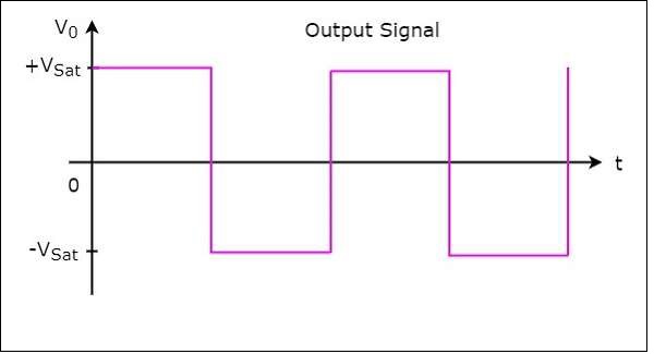
From the above figure we can observe that the output of square wave generator will have one of the two values: $+V_{sat}$ and $-V_{sat}$. So, the output remains at one value for some duration and then transitions to another value and remains there for some duration. In this way, it continues.
Triangular Wave Generator
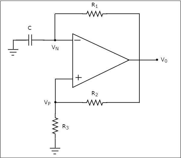
A triangular wave generator is an electronic circuit, which generates a triangular wave. The block diagram of a triangular wave generator is shown in the following figure −
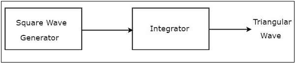
The block diagram of a triangular wave generator contains mainly two blocks: a square wave generator and an integrator. These two blocks are cascaded. That means, the output of square wave generator is applied as an input of integrator. Note that the integration of a square wave is nothing but a triangular wave.
The circuit diagram of an op-amp based triangular wave generator is shown in the following figure −
We have already seen the circuit diagrams of a square wave generator and an integrator. Observe that we got the above circuit diagram of an op-amp based triangular wave generator by replacing the blocks with the respective circuit diagrams in the block diagram of a triangular wave generator.
555 Timer
The 555 Timer IC got its name from the three $5K\Omega$ resistors that are used in its voltage divider network. This IC is useful for generating accurate time delays and oscillations. This chapter explains about 555 Timer in detail.
Pin Diagram and Functional Diagram
In this section, first let us discuss about the pin diagram of 555 Timer IC and then its functional diagram.
Pin Diagram
The 555 Timer IC is an 8 pin mini Dual-Inline Package (DIP). The pin diagram of a 555 Timer IC is shown in the following figure −
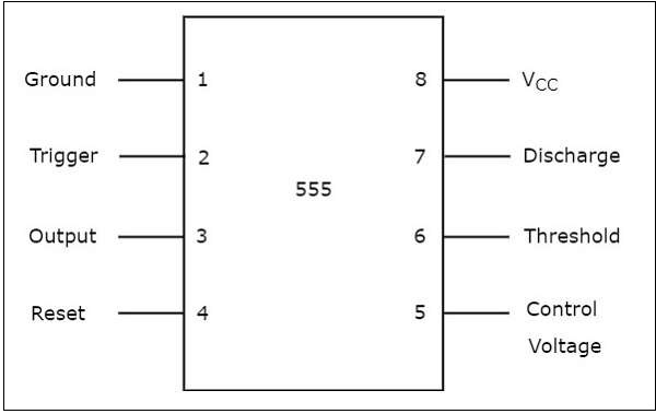
The significance of each pin is self-explanatory from the above diagram. This 555 Timer IC can be operated with a DC supply of +5V to +18V. It is mainly useful for generating non-sinusoidal wave forms like square, ramp, pulse & etc
Functional Diagram
The pictorial representation showing the internal details of a 555 Timer is known as functional diagram.
The functional diagram of 555 Timer IC is shown in the following figure −
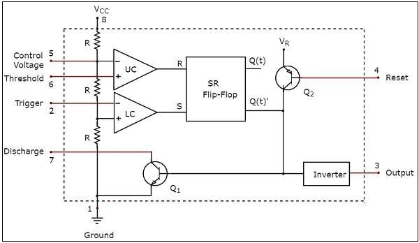
Observe that the functional diagram of 555 Timer contains a voltage divider network, two comparators, one SR flip-flop, two transistors and an inverter. This section discusses about the purpose of each block or component in detail −
Voltage Divider Network
The voltage divider network consists of a three $5K\Omega$ resistors that are connected in series between the supply voltage $V_{cc}$ and ground.
This network provides a voltage of $\frac{V_{cc} }{3}$ between a point and ground, if there exists only one $5K\Omega$ resistor. Similarly, it provides a voltage of $\frac{2V_{cc} }{3}$ between a point and ground, if there exists only two $5K\Omega$ resistors.
Comparator
The functional diagram of a 555 Timer IC consists of two comparators: an Upper Comparator (UC) and a Lower Comparator (LC).
Recall that a comparator compares the two inputs that are applied to it and produces an output.
If the voltage present at the non-inverting terminal of an op-amp is greater than the voltage present at its inverting terminal, then the output of comparator will be $+V_{sat}$. This can be considered as Logic High ('1') in digital representation.
If the voltage present at the non-inverting terminal of op-amp is less than or equal to the voltage at its inverting terminal, then the output of comparator will be $-V_{sat}$. This can be considered as Logic Low ('0') in digital representation.
SR Flip-Flop
Recall that a SR flip-flop operates with either positive clock transitions or negative clock transitions. It has two inputs: S and R, and two outputs: Q(t) and Q(t). The outputs, Q(t) & Q(t) are complement to each other.
The following table shows the state table of a SR flip-flop
| S | R | Q(t+1) |
|---|---|---|
| 0 | 0 | Q(t) |
| 0 | 1 | 0 |
| 1 | 0 | 1 |
| 1 | 1 | - |
Here, Q(t) & Q(t+1) are present state & next state respectively. So, SR flip-flop can be used for one of these three functions such as Hold, Reset & Set based on the input conditions, when positive (negative) transition of clock signal is applied.
The outputs of Lower Comparator (LC) and Upper Comparator (UC) are applied as inputs of SR flip-flop as shown in the functional diagram of 555 Timer IC.
Transistors and Inverter
The functional diagram of a 555 Timer IC consists of one npn transistor $Q_{1}$ and one pnp transistor $Q_{2}$. The npn transistor $Q_{1}$ will be turned ON if its base to emitter voltage is positive and greater than cut-in voltage. Otherwise, it will be turned-OFF.
The pnp transistor $Q_{2}$ is used as buffer in order to isolate the reset input from SR flip-flop and npn transistor $Q_{1}$.
The inverter used in the functional diagram of a 555 Timer IC not only performs the inverting action but also amplifies the power level.
The 555 Timer IC can be used in mono stable operation in order to produce a pulse at the output. Similarly, it can be used in astable operation in order to produce a square wave at the output.
Phase Locked Loop IC
Phase Locked Loop (PLL) is one of the vital blocks in linear systems. It is useful in communication systems such as radars, satellites, FMs, etc.
This chapter discusses about the block diagram of PLL and IC 565 in detail.
Block Diagram of PLL
A Phase Locked Loop (PLL) mainly consists of the following three blocks −
- Phase Detector
- Active Low Pass Filter
- Voltage Controlled Oscillator (VCO)
The block diagram of PLL is shown in the following figure −
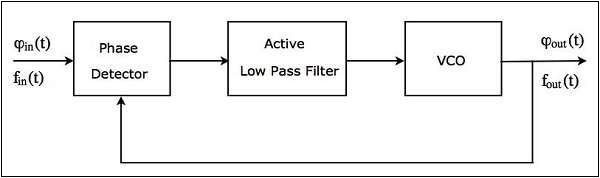
The output of a phase detector is applied as an input of active low pass filter. Similarly, the output of active low pass filter is applied as an input of VCO.
The working of a PLL is as follows −
Phase detector produces a DC voltage, which is proportional to the phase difference between the input signal having frequency of $f_{in}$ and feedback (output) signal having frequency of $f_{out}$.
A Phase detector is a multiplier and it produces two frequency components at its output − sum of the frequencies $f_{in}$ and $f_{out}$ and difference of frequencies $f_{in}$ & $f_{out}$.
An active low pass filter produces a DC voltage at its output, after eliminating high frequency component present in the output of the phase detector. It also amplifies the signal.
A VCO produces a signal having a certain frequency, when there is no input applied to it. This frequency can be shifted to either side by applying a DC voltage to it. Therefore, the frequency deviation is directly proportional to the DC voltage present at the output of a low pass filter.
The above operations take place until the VCO frequency equals to the input signal frequency. Based on the type of application, we can use either the output of active low pass filter or output of a VCO. PLLs are used in many applications such as FM demodulator, clock generator etc.
PLL operates in one of the following three modes −
- Free running mode
- Capture mode
- Lock mode
Initially, PLL operates in free running mode when no input is applied to it. When an input signal having some frequency is applied to PLL, then the output signal frequency of VCO will start change. At this stage, the PLL is said to be operating in the capture mode. The output signal frequency of VCO will change continuously until it is equal to the input signal frequency. Now, it is said to be PLL is operating in the lock mode.
IC 565
IC 565 is the most commonly used phase locked loop IC. It is a 14 pin Dual-Inline Package (DIP). The pin diagram of IC 565 is shown in the following figure −
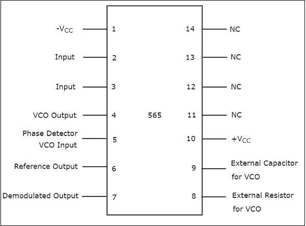
The purpose of each pin is self-explanatory from the above diagram. Out of 14 pins, only 10 pins (pin number 1 to 10) are utilized for the operation of PLL. So, the remaining 4 pins (pin number 11 to 14) are labelled with NC (No Connection).
The VCO produces an output at pin number 4 of IC 565, when the pin numbers 2 and 3 are grounded. Mathematically, we can write the output frequency, $f_{out}$ of the VCO as.
$$f_{out}=\frac{0.25}{R_VC_V}$$
where,
$R_{V}$ is the external resistor that is connected to the pin number 8
$C_{V}$ is the external capacitor that is connected to the pin number 9
By choosing proper values of $R_{V}$ and $C_{V}$, we can fix (determine) the output frequency, $f_{out}$ of VCO.
Pin numbers 4 and 5are to be shorted with an external wire so that the output of VCO can be applied as one of the inputs of phase detector.
IC 565 has an internal resistance of $3.6K\Omega$. A capacitor, C has to be connected between pin numbers 7 and 10 in order to make a low pass filter with that internal resistance.
Note that as per the requirement, we have to properly configure the pins of IC 565.
Voltage Regulators
The function of a voltage regulator is to maintain a constant DC voltage at the output irrespective of voltage fluctuations at the input and (or) variations in the load current. In other words, voltage regulator produces a regulated DC output voltage.
Voltage regulators are also available in Integrated Circuits (IC) forms. These are called as voltage regulator ICs.
Types of Voltage Regulators
There are two types of voltage regulators −
- Fixed voltage regulator
- Adjustable voltage regulator
This chapter discusses about these two types of voltage regulators one by one.
Fixed voltage regulator
A fixed voltage regulator produces a fixed DC output voltage, which is either positive or negative. In other words, some fixed voltage regulators produce positive fixed DC voltage values, while others produce negative fixed DC voltage values.
78xx voltage regulator ICs produce positive fixed DC voltage values, whereas, 79xx voltage regulator ICs produce negative fixed DC voltage values.
The following points are to be noted while working with 78xx and 79xx voltage regulator ICs −
xx corresponds to a two-digit number and represents the amount (magnitude) of voltage that voltage regulator IC produces.
Both 78xx and 79xx voltage regulator ICs have 3 pins each and the third pin is used for collecting the output from them.
The purpose of the first and second pins of these two types of ICs is different −
The first and second pins of 78xx voltage regulator ICs are used for connecting the input and ground respectively.
The first and second pins of 79xx voltage regulator ICs are used for connecting the ground and input respectively.
Examples
- 7805 voltage regulator IC produces a DC voltage of +5 volts.
- 7905 voltage regulator IC produces a DC voltage of -5 volts.
The following figure shows how to produce a fixed positive voltage at the output by using a fixed positive voltage regulator with necessary connections.
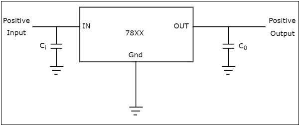
In the above figure that shows a fixed positive voltage regulator, the input capacitor Ci is used to prevent unwanted oscillations and the output capacitor, C0 acts as a line filter to improve transient response.
Note − an get a fixed negative voltage at the output by using a fixed negative voltage regulator with suitable connections.
Adjustable voltage regulator
An adjustable voltage regulator produces a DC output voltage, which can be adjusted to any other value of certain voltage range. Hence, adjustable voltage regulator is also called as a variable voltage regulator.
The DC output voltage value of an adjustable voltage regulator can be either positive or negative.
LM317 voltage regulator IC
LM317 voltage regulator IC can be used for producing a desired positive fixed DC voltage value of the available voltage range.
LM317 voltage regulator IC has 3 pins. The first pin is used for adjusting the output voltage, second pin is used for collecting the output and third pin is used for connecting the input.
The adjustable pin (terminal) is provided with a variable resistor which lets the output to vary between a wide range.
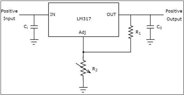
The above figure shows an unregulated power supply driving a LM 317 voltage regulator IC, which is commonly used. This IC can supply a load current of 1.5A over an adjustable output range of 1.25 V to 37 V.
Data Converters
All the real world quantities are analog in nature. We can represent these quantities electrically as analog signals. An analog signal is a time varying signal that has any number of values (variations) for a given time slot.
In contrast to this, a digital signal varies suddenly from one level to another level and will have only finite number of values (variations) for a given time slot.
This chapter discusses about the types of data converters and their specifications.
Types of Data Converters
The electronic circuits, which can be operated with analog signals are called as analog circuits. Similarly, the electronic circuits, which can be operated with digital signals are called as digital circuits. A data converter is an electronic circuit that converts data of one form to another.
There are two types of data converters −
- Analog to Digital Converter
- Digital to Analog Converter
If we want to connect the output of an analog circuit as an input of a digital circuit, then we have to place an interfacing circuit between them. This interfacing circuit that converts the analog signal into digital signal is called as Analog to Digital Converter.
Similarly, if we want to connect the output of a digital circuit as an input of an analog circuit, then we have to place an interfacing circuit between them. This interfacing circuit that converts the digital signal into an analog signal is called as Digital to Analog Converter.
Note that some Analog to Digital Converters may require Digital to Analog Converter as an internal block for their operation.
Specifications
The following are the specifications that are related to data conversions −
- Resolution
- Conversion Time
Resolution
Resolution is the minimum amount of change needed in an analog input voltage for it to be represented in binary (digital) output. It depends on the number of bits that are used in the digital output.
Mathematically, resolution can be represented as
$$Resolution=\frac{1}{2^{N}}$$
where, N is the number of bits that are present in the digital output.
From the above formula, we can observe that there exists an inverse relationship between the resolution and number of bits. Therefore, resolution decreases as the number of bits increases and vice-versa.
Resolution can also be defined as the ratio of maximum analog input voltage that can be represented in binary and the equivalent binary number.
Mathematically, resolution can be represented as
$$Resolution=\frac{V_{FS}}{2^{N}-1}$$
where,
$V_{FS}$ is the full scale input voltage or maximum analog input voltage,
N is the number of bits that are present in the digital output.
Conversion Time
The amount of time required for a data converter in order to convert the data (information) of one form into its equivalent data in other form is called as conversion time. Since we have two types of data converters, there are two types of conversion times as follows
- Analog to Digital Conversion time
- Digital to Analog Conversion time
The amount of time required for an Analog to Digital Converter (ADC) to convert the analog input voltage into its equivalent binary (digital) output is called as Analog to Digital conversion time. It depends on the number of bits that are used in the digital output.
The amount of time required for a Digital to Analog Converter (DAC) to convert the binary (digital) input into its equivalent analog output voltage is called as Digital to Analog conversion time. It depends on the number of bits that are present in the binary (digital) input.
Digital to Analog Converters
A Digital to Analog Converter (DAC) converts a digital input signal into an analog output signal. The digital signal is represented with a binary code, which is a combination of bits 0 and 1. This chapter deals with Digital to Analog Converters in detail.
The block diagram of DAC is shown in the following figure −
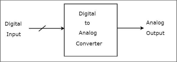
A Digital to Analog Converter (DAC) consists of a number of binary inputs and a single output. In general, the number of binary inputs of a DAC will be a power of two.
Types of DACs
There are two types of DACs
- Weighted Resistor DAC
- R-2R Ladder DAC
This section discusses about these two types of DACs in detail −
Weighted Resistor DAC
A weighted resistor DAC produces an analog output, which is almost equal to the digital (binary) input by using binary weighted resistors in the inverting adder circuit. In short, a binary weighted resistor DAC is called as weighted resistor DAC.
The circuit diagram of a 3-bit binary weighted resistor DAC is shown in the following figure −
Recall that the bits of a binary number can have only one of the two values. i.e., either 0 or 1. Let the 3-bit binary input is $b_{2}b_{1}b_{0}$. Here, the bits $b_{2}$ and $b_{0}$ denote the Most Significant Bit (MSB) and Least Significant Bit (LSB) respectively.
The digital switches shown in the above figure will be connected to ground, when the corresponding input bits are equal to 0. Similarly, the digital switches shown in the above figure will be connected to the negative reference voltage, $-V_{R}$ when the corresponding input bits are equal to 1.
In the above circuit, the non-inverting input terminal of an op-amp is connected to ground. That means zero volts is applied at the non-inverting input terminal of op-amp.
According to the virtual short concept, the voltage at the inverting input terminal of opamp is same as that of the voltage present at its non-inverting input terminal. So, the voltage at the inverting input terminals node will be zero volts.
The nodal equation at the inverting input terminals node is:
$$\frac{0+V_{R}b_{2}}{2^{0}R}+\frac{0+V_{R}b_{1}}{2^{1}R}+\frac{0+V_{R}b_{0}}{2^{2}R}+\frac{0-V_{0}}{R_{f}}=0$$
$$=>\frac{V_{0}}{R_{f}}=\frac{V_{R}b_{2}}{2^{0}R}+\frac{V_{R}b_{1}}{2^{1}R}+\frac{V_{R}b_{0}}{2^{2}R}$$
$$=>V_{0}=\frac{V_{R}R_{f}}{R}\left \{\frac{b_{2}}{2^{0}}+\frac{b_{1}}{2^{1}}+\frac{b_{0}}{2^{2}}\right \}$$
Substituting, $R=2R_{f}$ in above equation.
$$=>V_{0}=\frac{V_{R}R_{f}}{2R_{f}}\left \{\frac{b_{2}}{2^{0}}+\frac{b_{1}}{2^{1}}+\frac{b_{0}}{2^{2}}\right \}$$
$$=>V_{0}=\frac{V_{R}}{2}\left \{\frac{b_{2}}{2^{0}}+\frac{b_{1}}{2^{1}}+\frac{b_{0}}{2^{2}}\right \}$$
The above equation represents the output voltage equation of a 3-bit binary weighted resistor DAC. Since the number of bits are three in the binary (digital) input, we will get seven possible values of output voltage by varying the binary input from 000 to 111 for a fixed reference voltage, $V_{R}$.
We can write the generalized output voltage equation of an N-bit binary weighted resistor DAC as shown below based on the output voltage equation of a 3-bit binary weighted resistor DAC.
$$=>V_{0}=\frac{V_{R}}{2}\left \{ \frac{b_{N-1}}{2^{0}}+ \frac{b_{N-2}}{2^{1}}+....+\frac{b_{0}}{2^{N-1}} \right \}$$
The disadvantages of a binary weighted resistor DAC are as follows −
The difference between the resistance values corresponding to LSB & MSB will increase as the number of bits present in the digital input increases.
It is difficult to design more accurate resistors as the number of bits present in the digital input increases.
R-2R Ladder DAC
The R-2R Ladder DAC overcomes the disadvantages of a binary weighted resistor DAC. As the name suggests, R-2R Ladder DAC produces an analog output, which is almost equal to the digital (binary) input by using a R-2R ladder network in the inverting adder circuit.
Thecircuit diagramof a 3-bit R-2R Ladder DAC is shown in the following figure −
Recall that the bits of a binary number can have only one of the two values. i.e., either 0 or 1. Let the 3-bit binary input is $b_{2}b_{1}b_{0}$. Here, the bits $b_{2}$ and $b_{0}$ denote the Most Significant Bit (MSB) and Least Significant Bit (LSB) respectively.
The digital switches shown in the above figure will be connected to ground, when the corresponding input bits are equal to 0. Similarly, the digital switches shown in above figure will be connected to the negative reference voltage, $-V_{R}$ when the corresponding input bits are equal to 1.
It is difficult to get the generalized output voltage equation of a R-2R Ladder DAC. But, we can find the analog output voltage values of R-2R Ladder DAC for individual binary input combinations easily.
The advantages of a R-2R Ladder DAC are as follows −
R-2R Ladder DAC contains only two values of resistor: R and 2R. So, it is easy to select and design more accurate resistors.
If more number of bits are present in the digital input, then we have to include required number of R-2R sections additionally.
Due to the above advantages, R-2R Ladder DAC is preferable over binary weighted resistor DAC.
DAC Example Problem
In the previous chapter, we discussed the two types of DACs. This chapter discusses an example problem based on R-2R ladder DAC.
Example
Let us find the value of analog output voltage of R-2R Ladder DAC for a binary input, $b_{2}b_{1}b_{0}$ = 100.
Circuit Diagram and its Simplification
The circuit diagram of a 3-bit R-2R Ladder DAC when binary input, $b_{2}b_{1}b_{0}$ = 100 applied to it is shown in the following figure −
In the above circuit, there exists series and parallel combinations of resistors to the left of point A with respect to ground. So, we can replace that entire resistor network with a single resistor having resistance of $2R\Omega$.
The simplified circuit diagram is shown in the following figure −
We can replace the part of the network that is connected to the left of point B with respect to ground by using a Thevenins equivalent circuit. The modified circuit diagram is shown in the following figure −
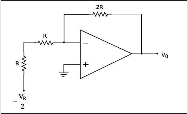
In the above circuit, there exist a series combination of two resistors. Replace this combination with a single resistor. The final circuit diagram after simplification is shown in the following figure −
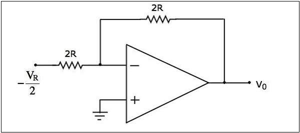
Now, the above circuit diagram looks like an inverting amplifier. It is having an input voltage of $-\frac{V_{R}}{2}$ volts, input resistance of $2R\Omega$ and feedback resistance of $2R\Omega$.
The output voltage of the circuit shown above will be −
$$V_{0}=-\frac{2R}{2R}\left(-\frac{V_{R}}{2}\right)$$
$$V_{0}=\frac{V_{R}}{2}$$
Therefore, the output voltage of 3-bit R-2R Ladder DAC is $\frac{V_{R}}{2}$ volts for a binary input, $b_{2}b_{1}b_{0}$ = 100.
Direct Type ADCs
An Analog to Digital Converter (ADC) converts an analog signal into a digital signal. The digital signal is represented with a binary code, which is a combination of bits 0 and 1.
The block diagram of an ADC is shown in the following figure −
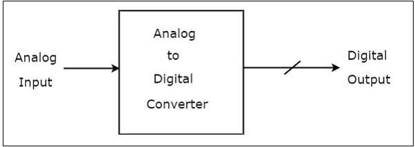
Observe that in the figure shown above, an Analog to Digital Converter (ADC) consists of a single analog input and many binary outputs. In general, the number of binary outputs of ADC will be a power of two.
There are two types of ADCs: Direct type ADCs and Indirect type ADC. This chapter discusses about the Direct type ADCs in detail.
If the ADC performs the analog to digital conversion directly by utilizing the internally generated equivalent digital (binary) code for comparing with the analog input, then it is called as Direct type ADC.
The following are the examples of Direct type ADCs −
- Counter type ADC
- Successive Approximation ADC
- Flash type ADC
This section discusses about these Direct type ADCs in detail.
Counter type ADC
A counter type ADC produces a digital output, which is approximately equal to the analog input by using counter operation internally.
The block diagram of a counter type ADC is shown in the following figure −
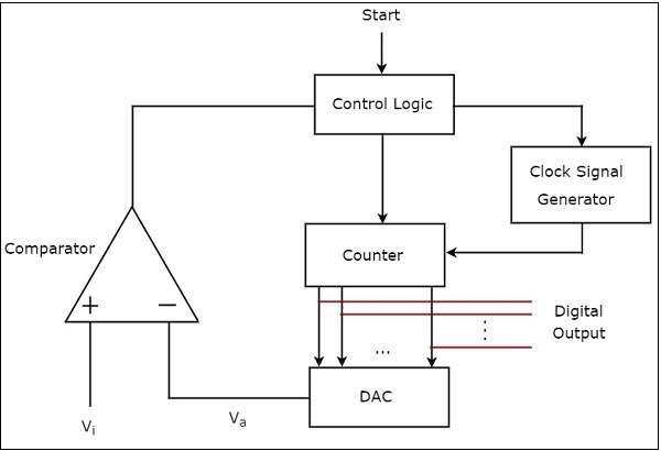
The counter type ADC mainly consists of 5 blocks: Clock signal generator, Counter, DAC, Comparator and Control logic.
The working of a counter type ADC is as follows −
The control logic resets the counter and enables the clock signal generator in order to send the clock pulses to the counter, when it received the start commanding signal.
The counter gets incremented by one for every clock pulse and its value will be in binary (digital) format. This output of the counter is applied as an input of DAC.
DAC converts the received binary (digital) input, which is the output of counter, into an analog output. Comparator compares this analog value,$V_{a}$ with the external analog input value $V_{i}$.
The output of comparator will be 1 as long as is greater than. The operations mentioned in above two steps will be continued as long as the control logic receives 1 from the output of comparator.
The output of comparator will be 0 when $V_{i}$ is less than or equal to $V_{a}$. So, the control logic receives 0 from the output of comparator. Then, the control logic disables the clock signal generator so that it doesnt send any clock pulse to the counter.
At this instant, the output of the counter will be displayed as the digital output. It is almost equivalent to the corresponding external analog input value $V_{i}$.
Successive Approximation ADC
A successive approximation type ADC produces a digital output, which is approximately equal to the analog input by using successive approximation technique internally.
The block diagram of a successive approximation ADC is shown in the following figure
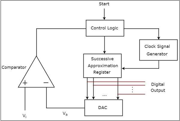
The successive approximation ADC mainly consists of 5 blocks− Clock signal generator, Successive Approximation Register (SAR), DAC, comparator and Control logic.
The working of a successive approximation ADC is as follows −
The control logic resets all the bits of SAR and enables the clock signal generator in order to send the clock pulses to SAR, when it received the start commanding signal.
The binary (digital) data present in SAR will be updated for every clock pulse based on the output of comparator. The output of SAR is applied as an input of DAC.
DAC converts the received digital input, which is the output of SAR, into an analog output. The comparator compares this analog value $V_{a}$ with the external analog input value $V_{i}$.
The output of a comparator will be 1 as long as $V_{i}$ is greater than $V_{a}$. Similarly, the output of comparator will be 0, when $V_{i}$ is less than or equal to $V_{a}$.
The operations mentioned in above steps will be continued until the digital output is a valid one.
The digital output will be a valid one, when it is almost equivalent to the corresponding external analog input value $V_{i}$.
Flash type ADC
A flash type ADC produces an equivalent digital output for a corresponding analog input in no time. Hence, flash type ADC is the fastest ADC.
The circuit diagram of a 3-bit flash type ADC is shown in the following figure −
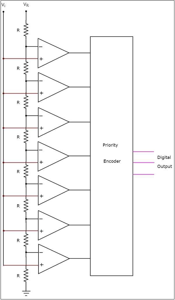
The 3-bit flash type ADC consists of a voltage divider network, 7 comparators and a priority encoder.
The working of a 3-bit flash type ADC is as follows.
The voltage divider networkcontains 8 equal resistors. A reference voltage $V_{R}$ is applied across that entire network with respect to the ground. The voltage drop across each resistor from bottom to top with respect to ground will be the integer multiples (from 1 to 8) of $\frac{V_{R}}{8}$.
The external input voltage $V_{i}$ is applied to the non-inverting terminal of all comparators. The voltage drop across each resistor from bottom to top with respect to ground is applied to the inverting terminal of comparators from bottom to top.
At a time, all the comparators compare the external input voltage with the voltage drops present at the respective other input terminal. That means, the comparison operations take place by each comparator parallelly.
The output of the comparator will be 1 as long as $V_{i}$ is greater than the voltage drop present at the respective other input terminal. Similarly, the output of comparator will be 0, when, $V_{i}$ is less than or equal to the voltage drop present at the respective other input terminal.
All the outputs of comparators are connected as the inputs of priority encoder.This priority encoder produces a binary code (digital output), which is corresponding to the high priority input that has 1.
Therefore, the output of priority encoder is nothing but the binary equivalent (digital output) of external analog input voltage, $V_{i}$.
The flash type ADC is used in the applications where the conversion speed of analog input into digital data should be very high.
Indirect type ADC
In the previous chapter, we discussed about what an ADC is and the examples of a Direct type ADC. This chapter discusses about the Indirect type ADC.
If an ADC performs the analog to digital conversion by an indirect method, then it is called an Indirect type ADC. In general, first it converts the analog input into a linear function of time (or frequency) and then it will produce the digital (binary) output.
Dual slope ADC is the best example of an Indirect type ADC. This chapter discusses about it in detail.
Dual Slope ADC
As the name suggests, a dual slope ADC produces an equivalent digital output for a corresponding analog input by using two (dual) slope technique.
The block diagram of a dual slope ADC is shown in the following figure −
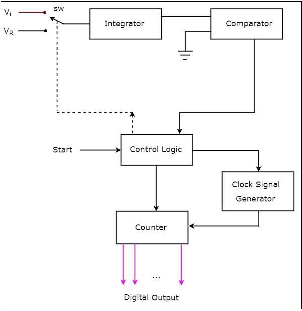
The dual slope ADC mainly consists of 5 blocks: Integrator, Comparator, Clock signal generator, Control logic and Counter.
The working of a dual slope ADC is as follows −
The control logic resets the counter and enables the clock signal generator in order to send the clock pulses to the counter, when it is received the start commanding signal.
Control logic pushes the switch sw to connect to the external analog input voltage $V_{i}$, when it is received the start commanding signal. This input voltage is applied to an integrator.
The output of the integrator is connected to one of the two inputs of the comparator and the other input of comparator is connected to ground.
Comparator compares the output of the integrator with zero volts (ground) and produces an output, which is applied to the control logic.
The counter gets incremented by one for every clock pulse and its value will be in binary (digital) format. It produces an overflow signal to the control logic, when it is incremented after reaching the maximum count value. At this instant, all the bits of counter will be having zeros only.
Now, the control logic pushes the switch sw to connect to the negative reference voltage $-V_{ref}$. This negative reference voltage is applied to an integrator. It removes the charge stored in the capacitor until it becomes zero.
At this instant, both the inputs of a comparator are having zero volts. So, comparator sends a signal to the control logic. Now, the control logic disables the clock signal generator and retains (holds) the counter value. The counter value is proportional to the external analog input voltage.
At this instant, the output of the counter will be displayed as the digital output. It is almost equivalent to the corresponding external analog input value $V_{i}$.
The dual slope ADC is used in the applications, where accuracy is more important while converting analog input into its equivalent digital (binary) data.
