- Home
- Basics of Integrated Circuits Applications
- Basics Operational Amplifier
- Op-Amp applications
- Arithmetic Circuits
- Differentiator & Integrator
- Converters Of Electrical Quantities
- Comparators
- Log & Anti-Log Amplifiers
- Rectifiers
- Clippers
- Clampers
- Active Filters
- Sinusoidal Oscillators
- Waveform Generators
- 555 Timer
- Phase Locked Loop Ic
- Voltage Regulators
- Data Converters
- Digital to Analog Converters
- DAC Example Problem
- Direct Type ADCs
- Indirect Type ADC
555 Timer
The 555 Timer IC got its name from the three $5K\Omega$ resistors that are used in its voltage divider network. This IC is useful for generating accurate time delays and oscillations. This chapter explains about 555 Timer in detail.
Pin Diagram and Functional Diagram
In this section, first let us discuss about the pin diagram of 555 Timer IC and then its functional diagram.
Pin Diagram
The 555 Timer IC is an 8 pin mini Dual-Inline Package (DIP). The pin diagram of a 555 Timer IC is shown in the following figure −
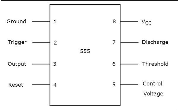
The significance of each pin is self-explanatory from the above diagram. This 555 Timer IC can be operated with a DC supply of +5V to +18V. It is mainly useful for generating non-sinusoidal wave forms like square, ramp, pulse & etc
Functional Diagram
The pictorial representation showing the internal details of a 555 Timer is known as functional diagram.
The functional diagram of 555 Timer IC is shown in the following figure −
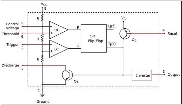
Observe that the functional diagram of 555 Timer contains a voltage divider network, two comparators, one SR flip-flop, two transistors and an inverter. This section discusses about the purpose of each block or component in detail −
Voltage Divider Network
The voltage divider network consists of a three $5K\Omega$ resistors that are connected in series between the supply voltage $V_{cc}$ and ground.
This network provides a voltage of $\frac{V_{cc} }{3}$ between a point and ground, if there exists only one $5K\Omega$ resistor. Similarly, it provides a voltage of $\frac{2V_{cc} }{3}$ between a point and ground, if there exists only two $5K\Omega$ resistors.
Comparator
The functional diagram of a 555 Timer IC consists of two comparators: an Upper Comparator (UC) and a Lower Comparator (LC).
Recall that a comparator compares the two inputs that are applied to it and produces an output.
If the voltage present at the non-inverting terminal of an op-amp is greater than the voltage present at its inverting terminal, then the output of comparator will be $+V_{sat}$. This can be considered as Logic High ('1') in digital representation.
If the voltage present at the non-inverting terminal of op-amp is less than or equal to the voltage at its inverting terminal, then the output of comparator will be $-V_{sat}$. This can be considered as Logic Low ('0') in digital representation.
SR Flip-Flop
Recall that a SR flip-flop operates with either positive clock transitions or negative clock transitions. It has two inputs: S and R, and two outputs: Q(t) and Q(t). The outputs, Q(t) & Q(t) are complement to each other.
The following table shows the state table of a SR flip-flop
| S | R | Q(t+1) |
|---|---|---|
| 0 | 0 | Q(t) |
| 0 | 1 | 0 |
| 1 | 0 | 1 |
| 1 | 1 | - |
Here, Q(t) & Q(t+1) are present state & next state respectively. So, SR flip-flop can be used for one of these three functions such as Hold, Reset & Set based on the input conditions, when positive (negative) transition of clock signal is applied.
The outputs of Lower Comparator (LC) and Upper Comparator (UC) are applied as inputs of SR flip-flop as shown in the functional diagram of 555 Timer IC.
Transistors and Inverter
The functional diagram of a 555 Timer IC consists of one npn transistor $Q_{1}$ and one pnp transistor $Q_{2}$. The npn transistor $Q_{1}$ will be turned ON if its base to emitter voltage is positive and greater than cut-in voltage. Otherwise, it will be turned-OFF.
The pnp transistor $Q_{2}$ is used as buffer in order to isolate the reset input from SR flip-flop and npn transistor $Q_{1}$.
The inverter used in the functional diagram of a 555 Timer IC not only performs the inverting action but also amplifies the power level.
The 555 Timer IC can be used in mono stable operation in order to produce a pulse at the output. Similarly, it can be used in astable operation in order to produce a square wave at the output.
