- Home
- Basics of Integrated Circuits Applications
- Basics Operational Amplifier
- Op-Amp applications
- Arithmetic Circuits
- Differentiator & Integrator
- Converters Of Electrical Quantities
- Comparators
- Log & Anti-Log Amplifiers
- Rectifiers
- Clippers
- Clampers
- Active Filters
- Sinusoidal Oscillators
- Waveform Generators
- 555 Timer
- Phase Locked Loop Ic
- Voltage Regulators
- Data Converters
- Digital to Analog Converters
- DAC Example Problem
- Direct Type ADCs
- Indirect Type ADC
Digital to Analog Converters
A Digital to Analog Converter (DAC) converts a digital input signal into an analog output signal. The digital signal is represented with a binary code, which is a combination of bits 0 and 1. This chapter deals with Digital to Analog Converters in detail.
The block diagram of DAC is shown in the following figure −
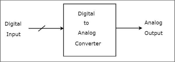
A Digital to Analog Converter (DAC) consists of a number of binary inputs and a single output. In general, the number of binary inputs of a DAC will be a power of two.
Types of DACs
There are two types of DACs
- Weighted Resistor DAC
- R-2R Ladder DAC
This section discusses about these two types of DACs in detail −
Weighted Resistor DAC
A weighted resistor DAC produces an analog output, which is almost equal to the digital (binary) input by using binary weighted resistors in the inverting adder circuit. In short, a binary weighted resistor DAC is called as weighted resistor DAC.
The circuit diagram of a 3-bit binary weighted resistor DAC is shown in the following figure −
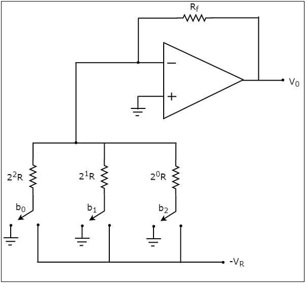
Recall that the bits of a binary number can have only one of the two values. i.e., either 0 or 1. Let the 3-bit binary input is $b_{2}b_{1}b_{0}$. Here, the bits $b_{2}$ and $b_{0}$ denote the Most Significant Bit (MSB) and Least Significant Bit (LSB) respectively.
The digital switches shown in the above figure will be connected to ground, when the corresponding input bits are equal to 0. Similarly, the digital switches shown in the above figure will be connected to the negative reference voltage, $-V_{R}$ when the corresponding input bits are equal to 1.
In the above circuit, the non-inverting input terminal of an op-amp is connected to ground. That means zero volts is applied at the non-inverting input terminal of op-amp.
According to the virtual short concept, the voltage at the inverting input terminal of opamp is same as that of the voltage present at its non-inverting input terminal. So, the voltage at the inverting input terminals node will be zero volts.
The nodal equation at the inverting input terminals node is:
$$\frac{0+V_{R}b_{2}}{2^{0}R}+\frac{0+V_{R}b_{1}}{2^{1}R}+\frac{0+V_{R}b_{0}}{2^{2}R}+\frac{0-V_{0}}{R_{f}}=0$$
$$=>\frac{V_{0}}{R_{f}}=\frac{V_{R}b_{2}}{2^{0}R}+\frac{V_{R}b_{1}}{2^{1}R}+\frac{V_{R}b_{0}}{2^{2}R}$$
$$=>V_{0}=\frac{V_{R}R_{f}}{R}\left \{\frac{b_{2}}{2^{0}}+\frac{b_{1}}{2^{1}}+\frac{b_{0}}{2^{2}}\right \}$$
Substituting, $R=2R_{f}$ in above equation.
$$=>V_{0}=\frac{V_{R}R_{f}}{2R_{f}}\left \{\frac{b_{2}}{2^{0}}+\frac{b_{1}}{2^{1}}+\frac{b_{0}}{2^{2}}\right \}$$
$$=>V_{0}=\frac{V_{R}}{2}\left \{\frac{b_{2}}{2^{0}}+\frac{b_{1}}{2^{1}}+\frac{b_{0}}{2^{2}}\right \}$$
The above equation represents the output voltage equation of a 3-bit binary weighted resistor DAC. Since the number of bits are three in the binary (digital) input, we will get seven possible values of output voltage by varying the binary input from 000 to 111 for a fixed reference voltage, $V_{R}$.
We can write the generalized output voltage equation of an N-bit binary weighted resistor DAC as shown below based on the output voltage equation of a 3-bit binary weighted resistor DAC.
$$=>V_{0}=\frac{V_{R}}{2}\left \{ \frac{b_{N-1}}{2^{0}}+ \frac{b_{N-2}}{2^{1}}+....+\frac{b_{0}}{2^{N-1}} \right \}$$
The disadvantages of a binary weighted resistor DAC are as follows −
The difference between the resistance values corresponding to LSB & MSB will increase as the number of bits present in the digital input increases.
It is difficult to design more accurate resistors as the number of bits present in the digital input increases.
R-2R Ladder DAC
The R-2R Ladder DAC overcomes the disadvantages of a binary weighted resistor DAC. As the name suggests, R-2R Ladder DAC produces an analog output, which is almost equal to the digital (binary) input by using a R-2R ladder network in the inverting adder circuit.
Thecircuit diagramof a 3-bit R-2R Ladder DAC is shown in the following figure −
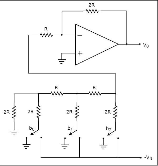
Recall that the bits of a binary number can have only one of the two values. i.e., either 0 or 1. Let the 3-bit binary input is $b_{2}b_{1}b_{0}$. Here, the bits $b_{2}$ and $b_{0}$ denote the Most Significant Bit (MSB) and Least Significant Bit (LSB) respectively.
The digital switches shown in the above figure will be connected to ground, when the corresponding input bits are equal to 0. Similarly, the digital switches shown in above figure will be connected to the negative reference voltage, $-V_{R}$ when the corresponding input bits are equal to 1.
It is difficult to get the generalized output voltage equation of a R-2R Ladder DAC. But, we can find the analog output voltage values of R-2R Ladder DAC for individual binary input combinations easily.
The advantages of a R-2R Ladder DAC are as follows −
R-2R Ladder DAC contains only two values of resistor: R and 2R. So, it is easy to select and design more accurate resistors.
If more number of bits are present in the digital input, then we have to include required number of R-2R sections additionally.
Due to the above advantages, R-2R Ladder DAC is preferable over binary weighted resistor DAC.
