- Home
- Basics of Integrated Circuits Applications
- Basics Operational Amplifier
- Op-Amp applications
- Arithmetic Circuits
- Differentiator & Integrator
- Converters Of Electrical Quantities
- Comparators
- Log & Anti-Log Amplifiers
- Rectifiers
- Clippers
- Clampers
- Active Filters
- Sinusoidal Oscillators
- Waveform Generators
- 555 Timer
- Phase Locked Loop Ic
- Voltage Regulators
- Data Converters
- Digital to Analog Converters
- DAC Example Problem
- Direct Type ADCs
- Indirect Type ADC
Phase Locked Loop IC
Phase Locked Loop (PLL) is one of the vital blocks in linear systems. It is useful in communication systems such as radars, satellites, FMs, etc.
This chapter discusses about the block diagram of PLL and IC 565 in detail.
Block Diagram of PLL
A Phase Locked Loop (PLL) mainly consists of the following three blocks −
- Phase Detector
- Active Low Pass Filter
- Voltage Controlled Oscillator (VCO)
The block diagram of PLL is shown in the following figure −
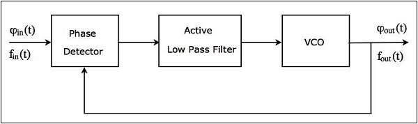
The output of a phase detector is applied as an input of active low pass filter. Similarly, the output of active low pass filter is applied as an input of VCO.
The working of a PLL is as follows −
Phase detector produces a DC voltage, which is proportional to the phase difference between the input signal having frequency of $f_{in}$ and feedback (output) signal having frequency of $f_{out}$.
A Phase detector is a multiplier and it produces two frequency components at its output − sum of the frequencies $f_{in}$ and $f_{out}$ and difference of frequencies $f_{in}$ & $f_{out}$.
An active low pass filter produces a DC voltage at its output, after eliminating high frequency component present in the output of the phase detector. It also amplifies the signal.
A VCO produces a signal having a certain frequency, when there is no input applied to it. This frequency can be shifted to either side by applying a DC voltage to it. Therefore, the frequency deviation is directly proportional to the DC voltage present at the output of a low pass filter.
The above operations take place until the VCO frequency equals to the input signal frequency. Based on the type of application, we can use either the output of active low pass filter or output of a VCO. PLLs are used in many applications such as FM demodulator, clock generator etc.
PLL operates in one of the following three modes −
- Free running mode
- Capture mode
- Lock mode
Initially, PLL operates in free running mode when no input is applied to it. When an input signal having some frequency is applied to PLL, then the output signal frequency of VCO will start change. At this stage, the PLL is said to be operating in the capture mode. The output signal frequency of VCO will change continuously until it is equal to the input signal frequency. Now, it is said to be PLL is operating in the lock mode.
IC 565
IC 565 is the most commonly used phase locked loop IC. It is a 14 pin Dual-Inline Package (DIP). The pin diagram of IC 565 is shown in the following figure −
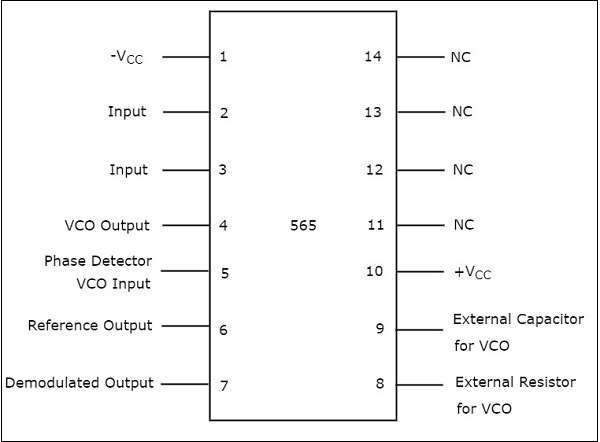
The purpose of each pin is self-explanatory from the above diagram. Out of 14 pins, only 10 pins (pin number 1 to 10) are utilized for the operation of PLL. So, the remaining 4 pins (pin number 11 to 14) are labelled with NC (No Connection).
The VCO produces an output at pin number 4 of IC 565, when the pin numbers 2 and 3 are grounded. Mathematically, we can write the output frequency, $f_{out}$ of the VCO as.
$$f_{out}=\frac{0.25}{R_VC_V}$$
where,
$R_{V}$ is the external resistor that is connected to the pin number 8
$C_{V}$ is the external capacitor that is connected to the pin number 9
By choosing proper values of $R_{V}$ and $C_{V}$, we can fix (determine) the output frequency, $f_{out}$ of VCO.
Pin numbers 4 and 5are to be shorted with an external wire so that the output of VCO can be applied as one of the inputs of phase detector.
IC 565 has an internal resistance of $3.6K\Omega$. A capacitor, C has to be connected between pin numbers 7 and 10 in order to make a low pass filter with that internal resistance.
Note that as per the requirement, we have to properly configure the pins of IC 565.