- Amplifiers Tutorial
- Amplifiers - Home
- Materials - Introduction
- Transistors
- Transistors - Overview
- Transistor Configurations
- Transistor Regions of Operation
- Transistor Load Line Analysis
- Operating Point
- Transistor as an Amplifier
- Transistor Biasing
- Methods of Transistor Biasing
- Bias Compensation
- Amplifiers
- Basic Amplifier
- Classification of Amplifiers
- Based on Configurations
- Multi-Stage Transistor Amplifier
- RC Coupling Amplifier
- Transformer Coupled Amplifier
- Direct Coupled Amplifier
- Power Amplifiers
- Classification of Power Amplifiers
- Class A Power Amplifiers
- Transformer Coupled Class A Power Amplifier
- Push-Pull Class A Power Amplifier
- Class B Power Amplifier
- Class AB and C Power Amplifiers
- Tuned Amplifiers
- Types of Tuned Amplifiers
- Feedback Amplifiers
- Negative Feedback Amplifiers
- Emitter Follower & Darlington Amplifier
- Noise in Amplifiers
- Amplifiers Useful Resources
- Amplifiers - Quick Guide
- Amplifiers - Useful Resources
- Amplifiers - Discussion
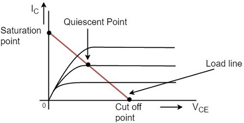
Operating Point
When a line is drawn joining the saturation and cut off points, such a line can be called as Load line. This line, when drawn over the output characteristic curve, makes contact at a point called as Operating point.
This operating point is also called as quiescent point or simply Q-point. There can be many such intersecting points, but the Q-point is selected in such a way that irrespective of AC signal swing, the transistor remains in the active region.
The following graph shows how to represent the operating point.
The operating point should not get disturbed as it should remain stable to achieve faithful amplification. Hence the quiescent point or Q-point is the value where the Faithful Amplification is achieved.
Faithful Amplification
The process of increasing the signal strength is called as Amplification. This amplification when done without any loss in the components of the signal, is called as Faithful amplification.
Faithful amplification is the process of obtaining complete portions of input signal by increasing the signal strength. This is done when AC signal is applied at its input.
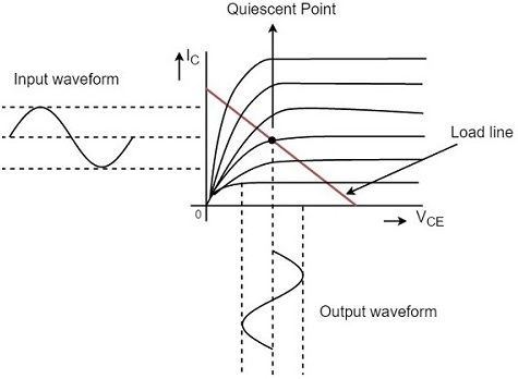
In the above graph, the input signal applied is completely amplified and reproduced without any losses. This can be understood as Faithful Amplification.
The operating point is so chosen such that it lies in the active region and it helps in the reproduction of complete signal without any loss.
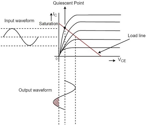
If the operating point is considered near saturation point, then the amplification will be as under.
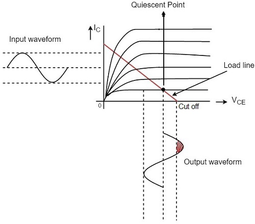
If the operation point is considered near cut off point, then the amplification will be as under.
Hence the placement of operating point is an important factor to achieve faithful amplification. But for the transistor to function properly as an amplifier, its input circuit (i.e., the base-emitter junction) remains forward biased and its output circuit (i.e., collector-base junction) remains reverse biased.
The amplified signal thus contains the same information as in the input signal whereas the strength of the signal is increased.
Key factors for Faithful Amplification
To ensure faithful amplification, the following basic conditions must be satisfied.
- Proper zero signal collector current
- Minimum proper base-emitter voltage (VBE) at any instant.
- Minimum proper collector-emitter voltage (VCE) at any instant.
The fulfillment of these conditions ensures that the transistor works over the active region having input forward biased and output reverse biased.
Proper Zero Signal Collector Current
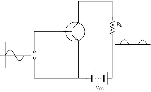
In order to understand this, let us consider a NPN transistor circuit as shown in the figure below. The base-emitter junction is forward biased and the collector-emitter junction is reverse biased. When a signal is applied at the input, the base-emitter junction of the NPN transistor gets forward biased for positive half cycle of the input and hence it appears at the output.
For negative half cycle, the same junction gets reverse biased and hence the circuit doesn’t conduct. This leads to unfaithful amplification as shown in the figure below.
Let us now introduce a battery VBB in the base circuit. The magnitude of this voltage should be such that the base-emitter junction of the transistor should remain in forward biased, even for negative half cycle of input signal. When no input signal is applied, a DC current flows in the circuit, due to VBB. This is known as zero signal collector current IC.
During the positive half cycle of the input, the base-emitter junction is more forward biased and hence the collector current increases. During the negative half cycle of the input, the input junction is less forward biased and hence the collector current decreases. Hence both the cycles of the input appear in the output and hence faithful amplification results, as shown in the below figure.
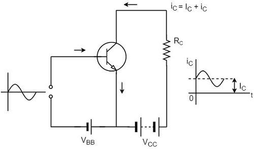
Hence for faithful amplification, proper zero signal collector current must flow. The value of zero signal collector current should be at least equal to the maximum collector current due to the signal alone.
Proper Minimum VBE at any instant
The minimum base to emitter voltage VBE should be greater than the cut-in voltage for the junction to be forward biased. The minimum voltage needed for a silicon transistor to conduct is 0.7v and for a germanium transistor to conduct is 0.5v. If the base-emitter voltage VBE is greater than this voltage, the potential barrier is overcome and hence the base current and collector currents increase sharply.
Hence if VBE falls low for any part of the input signal, that part will be amplified to a lesser extent due to the resultant small collector current, which results in unfaithful amplification.
Proper Minimum VCE at any instant
To achieve a faithful amplification, the collector emitter voltage VCE should not fall below the cut-in voltage, which is called as Knee Voltage. If VCE is lesser than the knee voltage, the collector base junction will not be properly reverse biased. Then the collector cannot attract the electrons which are emitted by the emitter and they will flow towards base which increases the base current. Thus the value of β falls.
Therefore, if VCE falls low for any part of the input signal, that part will be multiplied to a lesser extent, resulting in unfaithful amplification. So if VCE is greater than VKNEE the collector-base junction is properly reverse biased and the value of β remains constant, resulting in faithful amplification.