- Amplifiers Tutorial
- Amplifiers - Home
- Materials - Introduction
- Transistors
- Transistors - Overview
- Transistor Configurations
- Transistor Regions of Operation
- Transistor Load Line Analysis
- Operating Point
- Transistor as an Amplifier
- Transistor Biasing
- Methods of Transistor Biasing
- Bias Compensation
- Amplifiers
- Basic Amplifier
- Classification of Amplifiers
- Based on Configurations
- Multi-Stage Transistor Amplifier
- RC Coupling Amplifier
- Transformer Coupled Amplifier
- Direct Coupled Amplifier
- Power Amplifiers
- Classification of Power Amplifiers
- Class A Power Amplifiers
- Transformer Coupled Class A Power Amplifier
- Push-Pull Class A Power Amplifier
- Class B Power Amplifier
- Class AB and C Power Amplifiers
- Tuned Amplifiers
- Types of Tuned Amplifiers
- Feedback Amplifiers
- Negative Feedback Amplifiers
- Emitter Follower & Darlington Amplifier
- Noise in Amplifiers
- Amplifiers Useful Resources
- Amplifiers - Quick Guide
- Amplifiers - Useful Resources
- Amplifiers - Discussion
Amplifiers - Quick Guide
Materials - Introduction
Every material in nature has certain properties. These properties define the behavior of the materials. Material Science is a branch of electronics that deals with the study of flow of electrons in various materials or spaces, when they are subjected to various conditions.
Due to the intermixing of atoms in solids, instead of single energy levels, there will be bands of energy levels formed. These set of energy levels, which are closely packed are called as Energy bands.
Types of Materials
The energy band in which valence electrons are present is called Valence band, while the band in which conduction electrons are present is called Conduction band. The energy gap between these two bands is called as Forbidden energy gap.
Electronically, the materials are broadly classified as Insulators, Semiconductors, and Conductors.
Insulators − Insulators are such materials in which the conduction cannot take place, due to the large forbidden gap. Examples: Wood, Rubber.
Semiconductors − Semiconductors are such materials in which the forbidden energy gap is small and the conduction takes place if some external energy is applied. Examples: Silicon, Germanium.
Conductors − Conductors are such materials in which the forbidden energy gap disappears as the valence band and conduction band become very close that they overlap. Examples: Copper, Aluminum.
Of all the three, insulators are used where resistivity to electricity is desired and conductors are used where the conduction has to be high. The semiconductors are the ones which give rise to a specific interest of how they are used.
Semiconductors
A Semiconductor is a substance whose resistivity lies between the conductors and insulators. The property of resistivity is not the only one that decides a material as a semiconductor, but it has few properties as follows.
Semiconductors have the resistivity which is less than insulators and more than conductors.
Semiconductors have negative temperature co-efficient. The resistance in semiconductors, increases with the decrease in temperature and vice versa.
The Conducting properties of a Semi-conductor changes, when a suitable metallic impurity is added to it, which is a very important property.
The Semiconductor devices are extensively used in the field of electronics. The transistor has replaced the bulky vacuum tubes, from which the size and cost of the devices got decreased and this revolution has kept on increasing its pace leading to the new inventions like integrated electronics. Semiconductors can be classified as shown below.
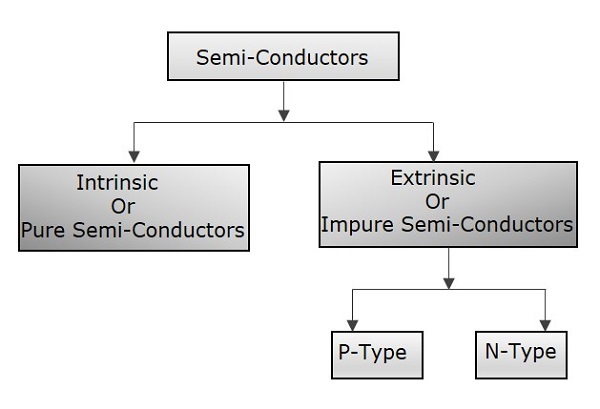
A semiconductor in its extremely pure form is said to be an intrinsic semiconductor. But the conduction capability of this pure form is too low. In order to increase the conduction capability of intrinsic semiconductor, it is better to add some impurities. This process of adding impurities is called as Doping. Now, this doped intrinsic semiconductor is called as an Extrinsic Semiconductor.
The impurities added, are generally pentavalent and trivalent impurities. Depending upon these types of impurities, another classification is done. When a pentavalent impurity is added to a pure semiconductor, it is called as N-type extrinsic Semiconductor. As well, when a trivalent impurity is added to a pure semiconductor, it is called as P-type extrinsic Semiconductor.
P-N Junction
When an electron moves from its place, a hole is said to be formed there. So, a hole is the absence of an electron. If an electron is said to be moved from negative to positive terminal, it means that a hole is being moved from positive to negative terminal.
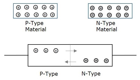
The materials mentioned above are the basics of semiconductor technology. The N-type material formed by adding pentavalent impurities has electrons as its majority carriers and holes as minority carriers. While, the P-type material formed by adding trivalent impurities has holes as its majority carriers and electrons as minority carriers.
Let us try to understand what happens when the P and N materials are joined together.
If a P-type and an N-type material are brought close to each other, both of them join to form a junction, as shown in the figure below.
A P-type material has holes as the majority carriers and an N-type material has electrons as the majority carriers. As opposite charges attract, few holes in P-type tend to go to n-side, whereas few electrons in N-type tend to go to P-side.
As both of them travel towards the junction, holes and electrons recombine with each other to neutralize and forms ions. Now, in this junction, there exists a region where the positive and negative ions are formed, called as PN junction or junction barrier as shown in the figure.
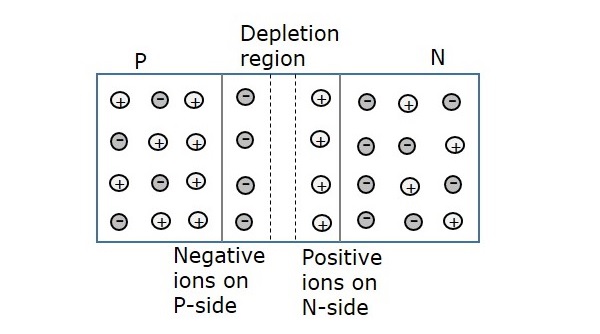
The formation of negative ions on P-side and positive ions on N-side results in the formation of a narrow charged region on either side of the PN junction. This region is now free from movable charge carriers. The ions present here have been stationary and maintain a region of space between them without any charge carriers.
As this region acts as a barrier between P and N type materials, this is also called as Barrier junction. This has another name called as Depletion region meaning it depletes both the regions. There occurs a potential difference VD due to the formation of ions, across the junction called as Potential Barrier as it prevents further movement of holes and electrons through the junction. This formation is called as a Diode.
Biasing of a Diode
When a diode or any two terminal components are connected in a circuit, it has two biased conditions with the given supply. They are Forward biased condition and Reverse biased condition.
Forward Biased Condition
When a diode is connected in a circuit, with its anode to the positive terminal and cathode to the negative terminal of the supply, then such a connection is said to be forward biased condition.
This kind of connection makes the circuit more and more forward biased and helps in more conduction. A diode conducts well in forward biased condition.
Reverse Biased Condition
When a diode is connected in a circuit, with its anode to the negative terminal and cathode to the positive terminal of the supply, then such a connection is said to be Reverse biased condition.
This kind of connection makes the circuit more and more reverse biased and helps in minimizing and preventing the conduction. A diode cannot conduct in reverse biased condition.
With the above information, we now have a good idea of what a PN junction is. With this knowledge, let us move on and learn about transistors in the next chapter.
Transistor - Overview
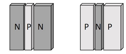
After knowing the details about a single PN junction, or simply a diode, let us try to go for the two PN junction connection. If another P-type material or N-type material is added to a single PN junction, another junction will be formed. Such a formation is simply called as a Transistor.
A Transistor is a three terminal semiconductor device that regulates current or voltage flow and acts as a switch or gate for signals.
Uses of a transistor
A transistor acts as an Amplifier, where the signal strength has to be increased.
A transistor also acts as a switch to choose between available options.
It also regulates the incoming current and voltage of the signals.
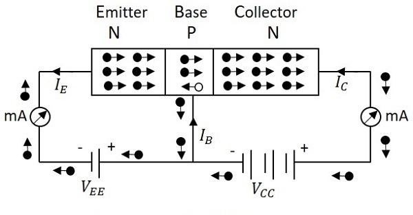
Constructional Details of a Transistor
The Transistor is a three terminal solid state device which is formed by connecting two diodes back to back. Hence it has got two PN junctions. Three terminals are drawn out of the three semiconductor materials present in it. This type of connection offers two types of transistors. They are PNP and NPN which means an N-type material between two Ptypes and the other is a P-type material between two N-types respectively.
The following illustration shows the basic construction of transistors
The three terminals drawn from the transistor indicate Emitter, Base and Collector terminals. They have their functionality as discussed below.
Emitter
The left-hand side of the above shown structure can be understood as Emitter.
This has a moderate size and is heavily doped as its main function is to supply a number of majority carriers, i.e. either electrons or holes.
As this emits electrons, it is called as an Emitter.
This is simply indicated with the letter E.
Base
The middle material in the above figure is the Base.
This is thin and lightly doped.
Its main function is to pass the majority carriers from the emitter to the collector.
This is indicated by the letter B.
Collector
The right side material in the above figure can be understood as a Collector.
Its name implies its function of collecting the carriers.
This is a bit larger in size than emitter and base. It is moderately doped.
This is indicated by the letter C.
The symbols of PNP and NPN transistors are as shown below.
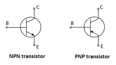
The arrow-head in the above figures indicated the emitter of a transistor. As the collector of a transistor has to dissipate much greater power, it is made large. Due to the specific functions of emitter and collector, they are not interchangeable. Hence the terminals are always to be kept in mind while using a transistor.
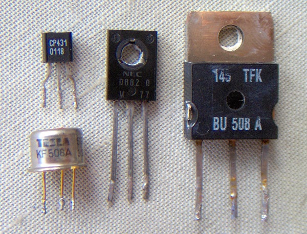
In a Practical transistor, there is a notch present near the emitter lead for identification. The PNP and NPN transistors can be differentiated using a Multimeter. The following image shows how different practical transistors look like.
We have so far discussed the constructional details of a transistor, but to understand the operation of a transistor, first we need to know about the biasing.
Transistor Biasing
As we know that a transistor is a combination of two diodes, we have two junctions here. As one junction is between the emitter and base, that is called as Emitter-Base junction and likewise, the other is Collector-Base junction.
Biasing is controlling the operation of the circuit by providing power supply. The function of both the PN junctions is controlled by providing bias to the circuit through some dc supply. The figure below shows how a transistor is biased.
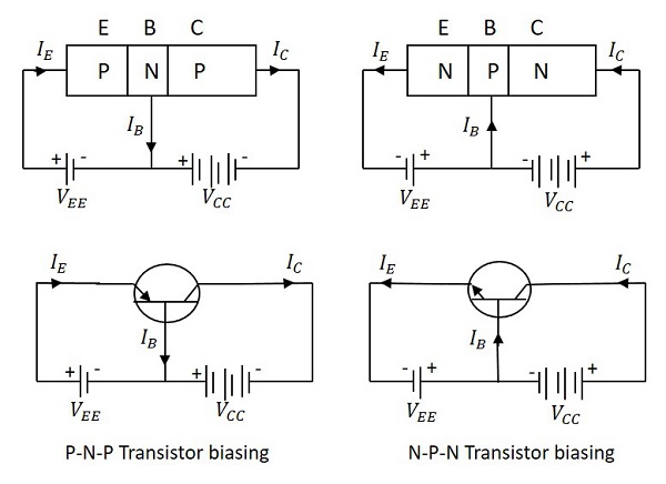
By having a look at the above figure, it is understood that
The N-type material is provided negative supply and P-type material is given positive supply to make the circuit Forward bias.
The N-type material is provided positive supply and P-type material is given negative supply to make the circuit Reverse bias.
By applying the power, the emitter base junction is always forward biased as the emitter resistance is very small. The collector base junction is reverse biased and its resistance is a bit higher. A small forward bias is sufficient at the emitter junction whereas a high reverse bias has to be applied at the collector junction.
The direction of current indicated in the circuits above, also called as the Conventional Current, is the movement of hole current which is opposite to the electron current.
Operation of PNP Transistor
The operation of a PNP transistor can be explained by having a look at the following figure, in which emitter-base junction is forward biased and collector-base junction is reverse biased.
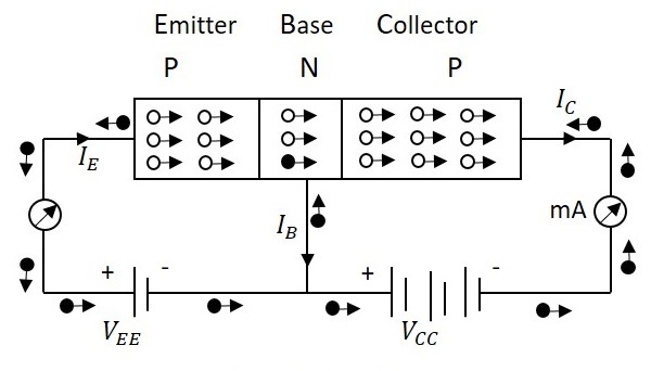
The voltage VEE provides a positive potential at the emitter which repels the holes in the P-type material and these holes cross the emitter-base junction, to reach the base region. There a very low percent of holes re-combine with free electrons of N-region. This provides very low current which constitutes the base current IB. The remaining holes cross the collector-base junction, to constitute collector current IC, which is the hole current.
As a hole reaches the collector terminal, an electron from the battery negative terminal fills the space in the collector. This flow slowly increases and the electron minority current flows through the emitter, where each electron entering the positive terminal of VEE, is replaced by a hole by moving towards the emitter junction. This constitutes emitter current IE.
Hence we can understand that −
The conduction in a PNP transistor takes place through holes.
The collector current is slightly less than the emitter current.
The increase or decrease in the emitter current affects the collector current.
Operation of NPN Transistor
The operation of an NPN transistor can be explained by having a look at the following figure, in which emitter-base junction is forward biased and collector-base junction is reverse biased.
The voltage VEE provides a negative potential at the emitter which repels the electrons in the N-type material and these electrons cross the emitter-base junction, to reach the base region. There, a very low percent of electrons re-combine with free holes of P-region. This provides very low current which constitutes the base current IB. The remaining holes cross the collector-base junction, to constitute the collector current IC.
As an electron reaches out of the collector terminal, and enters the positive terminal of the battery, an electron from the negative terminal of the battery VEE enters the emitter region. This flow slowly increases and the electron current flows through the transistor.
Hence we can understand that −
The conduction in a NPN transistor takes place through electrons.
The collector current is higher than the emitter current.
The increase or decrease in the emitter current affects the collector current.
Advantages of Transistors
There are many advantages of using a transistor, such as −
- High voltage gain.
- Lower supply voltage is sufficient.
- Most suitable for low power applications.
- Smaller and lighter in weight.
- Mechanically stronger than vacuum tubes.
- No external heating required like vacuum tubes.
- Very suitable to integrate with resistors and diodes to produce ICs.
There are few disadvantages such as they cannot be used for high power applications due to lower power dissipation. They have lower input impedance and they are temperature dependent.
Transistor Configurations
Any transistor has three terminals, the emitter, the base, and the collector. Using these 3 terminals the transistor can be connected in a circuit with one terminal common to both input and output in three different possible configurations.
The three types of configurations are Common Base, Common Emitter and Common Collector configurations. In every configuration, the emitter junction is forward biased and the collector junction is reverse biased.
Common Base (CB) Configuration
The name itself implies that the Base terminal is taken as common terminal for both input and output of the transistor. The common base connection for both NPN and PNP transistors is as shown in the following figure.
For the sake of understanding, let us consider NPN transistor in CB configuration. When the emitter voltage is applied, as it is forward biased, the electrons from the negative terminal repel the emitter electrons and current flows through the emitter and base to the collector to contribute collector current. The collector voltage VCB is kept constant throughout this.
In the CB configuration, the input current is the emitter current IE and the output current is the collector current IC.
Current Amplification Factor (α)
The ratio of change in collector current (ΔIC) to the change in emitter current (ΔIE) when collector voltage VCB is kept constant, is called as Current amplification factor. It is denoted by α.
$\alpha = \frac{\Delta I_C}{\Delta I_E}$ at constant VCB
Expression for Collector current
With the above idea, let us try to draw some expression for collector current.
Along with the emitter current flowing, there is some amount of base current IB which flows through the base terminal due to electron hole recombination. As collector-base junction is reverse biased, there is another current which is flown due to minority charge carriers. This is the leakage current which can be understood as Ileakage. This is due to minority charge carriers and hence very small.
The emitter current that reaches the collector terminal is
$$\alpha I_E$$
Total collector current
$$I_C = \alpha I_E + I_{leakage}$$
If the emitter-base voltage VEB = 0, even then, there flows a small leakage current, which can be termed as ICBO (collector-base current with output open).
The collector current therefore can be expressed as
$$I_C = \alpha I_E + I_{CBO}$$
$$I_E = I_C + I_B$$
$$I_C = \alpha (I_C + I_B) + I_{CBO}$$
$$I_C (1 - \alpha) = \alpha I_B + I_{CBO}$$
$$I_C = \frac{\alpha}{1 - \alpha}I_B + \frac{I_{CBO}}{1 - \alpha}$$
$$I_C = \left ( \frac{\alpha}{1 - \alpha} \right )I_B + \left ( \frac{1}{1 - \alpha} \right )I_{CBO}$$
Hence the above derived is the expression for collector current. The value of collector current depends on base current and leakage current along with the current amplification factor of that transistor in use.
Characteristics of CB configuration
This configuration provides voltage gain but no current gain.
Being VCB constant, with a small increase in the Emitter-base voltage VEB, Emitter current IE gets increased.
Emitter Current IE is independent of Collector voltage VCB.
Collector Voltage VCB can affect the collector current IC only at low voltages, when VEB is kept constant.
The input resistance Ri is the ratio of change in emitter-base voltage (ΔVEB) to the change in emitter current (ΔIE) at constant collector base voltage VCB.
$R_i = \frac{\Delta V_{EB}}{\Delta I_E}$ at constant VCB
As the input resistance is of very low value, a small value of VEB is enough to produce a large current flow of emitter current IE.
The output resistance Ro is the ratio of change in the collector base voltage (ΔVCB) to the change in collector current (ΔIC) at constant emitter current IE.
$R_o = \frac{\Delta V_{CB}}{\Delta I_C}$ at constant IE
As the output resistance is of very high value, a large change in VCB produces a very little change in collector current IC.
This Configuration provides good stability against increase in temperature.
The CB configuration is used for high frequency applications.
Common Emitter (CE) Configuration
The name itself implies that the Emitter terminal is taken as common terminal for both input and output of the transistor. The common emitter connection for both NPN and PNP transistors is as shown in the following figure.
Just as in CB configuration, the emitter junction is forward biased and the collector junction is reverse biased. The flow of electrons is controlled in the same manner. The input current is the base current IB and the output current is the collector current IC here.
Base Current Amplification factor (β)
The ratio of change in collector current (ΔIC) to the change in base current (ΔIB) is known as Base Current Amplification Factor. It is denoted by β.
$$\beta = \frac{\Delta I_C}{\Delta I_B}$$
Relation between β and α
Let us try to derive the relation between base current amplification factor and emitter current amplification factor.
$$\beta = \frac{\Delta I_C}{\Delta I_B}$$
$$\alpha = \frac{\Delta I_C}{\Delta I_E}$$
$$I_E = I_B + I_C$$
$$\Delta I_E = \Delta I_B + \Delta I_C$$
$$\Delta I_B = \Delta I_E - \Delta I_C$$
We can write
$$\beta = \frac{\Delta I_C}{\Delta I_E - \Delta I_C}$$
Dividing by ΔIE
$$\beta = \frac{\Delta I_C/\Delta I_E}{\frac{\Delta I_E}{\Delta I_E} - \frac{\Delta I_C}{\Delta I_E}}$$
We have
$$\alpha = \Delta I_C / \Delta I_E$$
Therefore,
$$\beta = \frac{\alpha}{1 - \alpha}$$
From the above equation, it is evident that, as α approaches 1, β reaches infinity.
Hence, the current gain in Common Emitter connection is very high. This is the reason this circuit connection is mostly used in all transistor applications.
Expression for Collector Current
In the Common Emitter configuration, IB is the input current and IC is the output current.
We know
$$I_E = I_B + I_C$$
And
$$I_C = \alpha I_E + I_{CBO}$$
$$= \alpha(I_B + I_C) + I_{CBO}$$
$$I_C(1 - \alpha) = \alpha I_B + I_{CBO}$$
$$I_C = \frac{\alpha}{1 - \alpha}I_B + \frac{1}{1 - \alpha}I_{CBO}$$
If base circuit is open, i.e. if IB = 0,
The collector emitter current with base open is ICEO
$$I_{CEO} = \frac{1}{1 - \alpha}I_{CBO}$$
Substituting the value of this in the previous equation, we get
$$I_C = \frac{\alpha}{1 - \alpha}I_B + I_{CEO}$$
$$I_C = \beta I_B + I_{CEO}$$
Hence the equation for collector current is obtained.
Knee Voltage
In CE configuration, by keeping the base current IB constant, if VCE is varied, IC increases nearly to 1v of VCE and stays constant thereafter. This value of VCE up to which collector current IC changes with VCE is called the Knee Voltage. The transistors while operating in CE configuration, they are operated above this knee voltage.
Characteristics of CE Configuration
This configuration provides good current gain and voltage gain.
Keeping VCE constant, with a small increase in VBE the base current IB increases rapidly than in CB configurations.
For any value of VCE above knee voltage, IC is approximately equal to βIB.
The input resistance Ri is the ratio of change in base emitter voltage (ΔVBE) to the change in base current (ΔIB) at constant collector emitter voltage VCE.
$R_i = \frac{\Delta V_{BE}}{\Delta I_B}$ at constant VCE
As the input resistance is of very low value, a small value of VBE is enough to produce a large current flow of base current IB.
The output resistance Ro is the ratio of change in collector emitter voltage (ΔVCE) to the change in collector current (ΔIC) at constant IB.
$R_o = \frac{\Delta V_{CE}}{\Delta I_C}$ at constant IB
As the output resistance of CE circuit is less than that of CB circuit.
This configuration is usually used for bias stabilization methods and audio frequency applications.
Common Collector (CC) Configuration
The name itself implies that the Collector terminal is taken as common terminal for both input and output of the transistor. The common collector connection for both NPN and PNP transistors is as shown in the following figure.
Just as in CB and CE configurations, the emitter junction is forward biased and the collector junction is reverse biased. The flow of electrons is controlled in the same manner. The input current is the base current IB and the output current is the emitter current IE here.
Current Amplification Factor (γ)
The ratio of change in emitter current (ΔIE) to the change in base current (ΔIB) is known as Current Amplification factor in common collector (CC) configuration. It is denoted by γ.
$$\gamma = \frac{\Delta I_E}{\Delta I_B}$$
- The current gain in CC configuration is same as in CE configuration.
- The voltage gain in CC configuration is always less than 1.
Relation between γ and α
Let us try to draw some relation between γ and α
$$\gamma = \frac{\Delta I_E}{\Delta I_B}$$
$$\alpha = \frac{\Delta I_C}{\Delta I_E}$$
$$I_E = I_B + I_C$$
$$\Delta I_E = \Delta I_B + \Delta I_C$$
$$\Delta I_B = \Delta I_E - \Delta I_C$$
Substituting the value of IB, we get
$$\gamma = \frac{\Delta I_E}{\Delta I_E - \Delta I_C}$$
Dividing by ΔIE
$$\gamma = \frac{\Delta I_E / \Delta I_E}{\frac{\Delta I_E}{\Delta I_E} - \frac{\Delta I_C}{\Delta I_E}}$$
$$= \frac{1}{1 - \alpha}$$
$$\gamma = \frac{1}{1 - \alpha}$$
Expression for collector current
We know
$$I_C = \alpha I_E + I_{CBO}$$
$$I_E = I_B + I_C = I_B + (\alpha I_E + I_{CBO})$$
$$I_E(1 - \alpha) = I_B + I_{CBO}$$
$$I_E = \frac{I_B}{1 - \alpha} + \frac{I_{CBO}}{1 - \alpha}$$
$$I_C \cong I_E = (\beta + 1)I_B + (\beta + 1)I_{CBO}$$
The above is the expression for collector current.
Characteristics of CC Configuration
This configuration provides current gain but no voltage gain.
In CC configuration, the input resistance is high and the output resistance is low.
The voltage gain provided by this circuit is less than 1.
The sum of collector current and base current equals emitter current.
The input and output signals are in phase.
This configuration works as non-inverting amplifier output.
This circuit is mostly used for impedance matching. That means, to drive a low impedance load from a high impedance source.
Transistor Regions of Operation
The DC supply is provided for the operation of a transistor. This DC supply is given to the two PN junctions of a transistor which influences the actions of majority carriers in these emitter and collector junctions.
The junctions are forward biased and reverse biased based on our requirement. Forward biased is the condition where a positive voltage is applied to the p-type and negative voltage is applied to the n-type material. Reverse biased is the condition where a positive voltage is applied to the n-type and negative voltage is applied to the p-type material.
Transistor Biasing
The supply of suitable external dc voltage is called as biasing. Either forward or reverse biasing is done to the emitter and collector junctions of the transistor.
These biasing methods make the transistor circuit to work in four kinds of regions such as Active region, Saturation region, Cutoff region and Inverse active region (seldom used). This is understood by having a look at the following table.
| Emitter Junction | Collector Junction | Region of Operation |
|---|---|---|
| Forward biased | Forward biased | Saturation region |
| Forward biased | Reverse biased | Active region |
| Reverse biased | Forward biased | Inverse active region |
| Reverse biased | Reverse biased | Cut off region |
Among these regions, Inverse active region, which is just the inverse of active region, is not suitable for any applications and hence not used.
Active Region
This is the region in which transistors have many applications. This is also called as linear region. A transistor while in this region, acts better as an Amplifier.
The following circuit diagram shows a transistor working in active region.
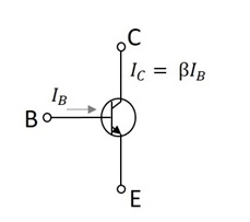
This region lies between saturation and cutoff. The transistor operates in active region when the emitter junction is forward biased and collector junction is reverse biased.
In the active state, collector current is β times the base current, i.e.
$$I_C = \beta I_B$$
Where IC = collector current, β = current amplification factor, and IB = base current.
Saturation Region
This is the region in which transistor tends to behave as a closed switch. The transistor has the effect of its collector and emitter being shorted. The collector and emitter currents are maximum in this mode of operation.
The following figure shows a transistor working in saturation region.
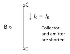
The transistor operates in saturation region when both the emitter and collector junctions are forward biased.
In saturation mode,
$$\beta < \frac{I_C}{I_B}$$
As in the saturation region the transistor tends to behave as a closed switch,
$$I_C = I_E$$
Where IC = collector current and IE = emitter current.
Cutoff Region
This is the region in which transistor tends to behave as an open switch. The transistor has the effect of its collector and base being opened. The collector, emitter and base currents are all zero in this mode of operation.
The figure below shows a transistor working in cutoff region.
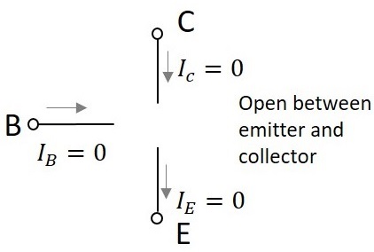
The transistor operates in cutoff region when both the emitter and collector junctions are reverse biased.
As in cutoff region, the collector current, emitter current and base currents are nil, we can write as
$$I_C = I_E = I_B = 0$$
Where IC = collector current, IE = emitter current, and IB = base current.
Transistor Load Line Analysis
Till now we have discussed different regions of operation for a transistor. But among all these regions, we have found that the transistor operates well in active region and hence it is also called as linear region. The outputs of the transistor are the collector current and collector voltages.
Output Characteristics
When the output characteristics of a transistor are considered, the curve looks as below for different input values.
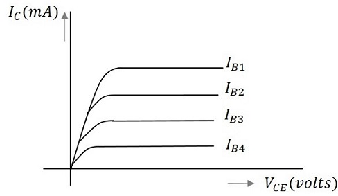
In the above figure, the output characteristics are drawn between collector current IC and collector voltage VCE for different values of base current IB. These are considered here for different input values to obtain different output curves.
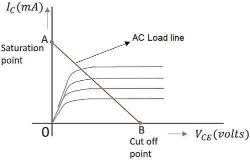
Load Line
When a value for the maximum possible collector current is considered, that point will be present on the Y-axis, which is nothing but the Saturation point. As well, when a value for the maximum possible collector emitter voltage is considered, that point will be present on the X-axis, which is the Cutoff point.
When a line is drawn joining these two points, such a line can be called as Load line. This is called so as it symbolizes the output at the load. This line, when drawn over the output characteristic curve, makes contact at a point called as Operating point or quiescent point or simply Q-point.
The concept of load line can be understood from the following graph.
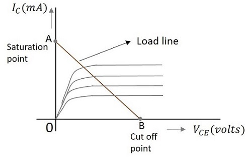
The load line is drawn by joining the saturation and cut off points. The region that lies between these two is the linear region. A transistor acts as a good amplifier in this linear region.
If this load line is drawn only when DC biasing is given to the transistor, but no input signal is applied, then such a load line is called as DC load line. Whereas the load line drawn under the conditions when an input signal along with the DC voltages are applied, such a line is called as an AC load line.
DC Load Line
When the transistor is given the bias and no signal is applied at its input, the load line drawn under such conditions, can be understood as DC condition. Here there will be no amplification as the signal is absent. The circuit will be as shown below.
The value of collector emitter voltage at any given time will be
$$V_{CE} = V_{CC} - I_C R_C$$
As VCC and RC are fixed values, the above one is a first degree equation and hence will be a straight line on the output characteristics. This line is called as D.C. Load line. The figure below shows the DC load line.
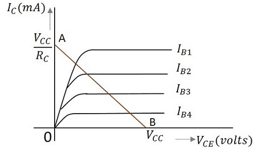
To obtain the load line, the two end points of the straight line are to be determined. Let those two points be A and B.
To obtain A
When collector emitter voltage VCE = 0, the collector current is maximum and is equal to VCC/RC. This gives the maximum value of VCE. This is shown as
$$V_{CE} = V_{CC} - I_C R_C$$
$$0 = V_{CC} - I_C R_C$$
$$I_C = V_{CC}/R_C$$
This gives the point A (OA = VCC/RC) on collector current axis, shown in the above figure.
To obtain B
When the collector current IC = 0, then collector emitter voltage is maximum and will be equal to the VCC. This gives the maximum value of IC. This is shown as
$$V_{CE} = V_{CC} - I_C R_C$$
$$= V_{CC}$$
(AS IC = 0)
This gives the point B, which means (OB = VCC) on the collector emitter voltage axis shown in the above figure.
Hence we got both the saturation and cutoff point determined and learnt that the load line is a straight line. So, a DC load line can be drawn.
AC Load Line
The DC load line discussed previously, analyzes the variation of collector currents and voltages, when no AC voltage is applied. Whereas the AC load line gives the peak-to-peak voltage, or the maximum possible output swing for a given amplifier.
We shall consider an AC equivalent circuit of a CE amplifier for our understanding.
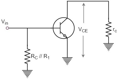
From the above figure,
$$V_{CE} = (R_C // R_1) \times I_C$$
$$r_C = R_C // R_1$$
For a transistor to operate as an amplifier, it should stay in active region. The quiescent point is so chosen in such a way that the maximum input signal excursion is symmetrical on both negative and positive half cycles.
Hence,
$V_{max} = V_{CEQ}$ and $V_{min} = -V_{CEQ}$
Where VCEQ is the emitter-collector voltage at quiescent point
The following graph represents the AC load line which is drawn between saturation and cut off points.
From the graph above, the current IC at the saturation point is
$$I_{C(sat)} = I_{CQ} + (V_{CEQ}/r_C)$$
The voltage VCE at the cutoff point is
$$V_{CE(off)} = V_{CEQ} + I_{CQ}r_C$$
Hence the maximum current for that corresponding VCEQ = VCEQ / (RC // R1) is
$$I_{CQ} = I_{CQ} * (R_C // R_1)$$
Hence by adding quiescent currents the end points of AC load line are
$$I_{C(sat)} = I_{CQ} + V_{CEQ}/ (R_C // R_1)$$
$$V_{CE(off)} = V_{CEQ} + I_{CQ} * (R_C // R_1)$$
AC and DC Load Line
When AC and DC Load lines are represented in a graph, it can be understood that they are not identical. Both of these lines intersect at the Q-point or quiescent point. The endpoints of AC load line are saturation and cut off points. This is understood from the figure below.
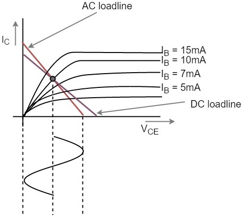
From the above figure, it is understood that the quiescent point (the dark dot) is obtained when the value of base current IB is 10mA. This is the point where both the AC and DC load lines intersect.
In the next chapter, we will discuss the concept of quiescent point or the operating point in detail.
Operating Point
When a line is drawn joining the saturation and cut off points, such a line can be called as Load line. This line, when drawn over the output characteristic curve, makes contact at a point called as Operating point.
This operating point is also called as quiescent point or simply Q-point. There can be many such intersecting points, but the Q-point is selected in such a way that irrespective of AC signal swing, the transistor remains in the active region.
The following graph shows how to represent the operating point.
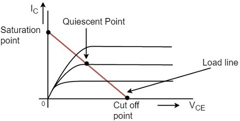
The operating point should not get disturbed as it should remain stable to achieve faithful amplification. Hence the quiescent point or Q-point is the value where the Faithful Amplification is achieved.
Faithful Amplification
The process of increasing the signal strength is called as Amplification. This amplification when done without any loss in the components of the signal, is called as Faithful amplification.
Faithful amplification is the process of obtaining complete portions of input signal by increasing the signal strength. This is done when AC signal is applied at its input.
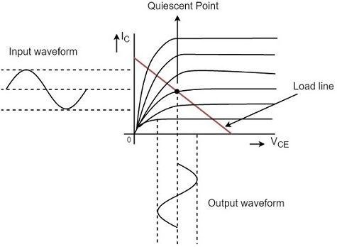
In the above graph, the input signal applied is completely amplified and reproduced without any losses. This can be understood as Faithful Amplification.
The operating point is so chosen such that it lies in the active region and it helps in the reproduction of complete signal without any loss.
If the operating point is considered near saturation point, then the amplification will be as under.
If the operation point is considered near cut off point, then the amplification will be as under.
Hence the placement of operating point is an important factor to achieve faithful amplification. But for the transistor to function properly as an amplifier, its input circuit (i.e., the base-emitter junction) remains forward biased and its output circuit (i.e., collector-base junction) remains reverse biased.
The amplified signal thus contains the same information as in the input signal whereas the strength of the signal is increased.
Key factors for Faithful Amplification
To ensure faithful amplification, the following basic conditions must be satisfied.
- Proper zero signal collector current
- Minimum proper base-emitter voltage (VBE) at any instant.
- Minimum proper collector-emitter voltage (VCE) at any instant.
The fulfillment of these conditions ensures that the transistor works over the active region having input forward biased and output reverse biased.
Proper Zero Signal Collector Current
In order to understand this, let us consider a NPN transistor circuit as shown in the figure below. The base-emitter junction is forward biased and the collector-emitter junction is reverse biased. When a signal is applied at the input, the base-emitter junction of the NPN transistor gets forward biased for positive half cycle of the input and hence it appears at the output.
For negative half cycle, the same junction gets reverse biased and hence the circuit doesn’t conduct. This leads to unfaithful amplification as shown in the figure below.
Let us now introduce a battery VBB in the base circuit. The magnitude of this voltage should be such that the base-emitter junction of the transistor should remain in forward biased, even for negative half cycle of input signal. When no input signal is applied, a DC current flows in the circuit, due to VBB. This is known as zero signal collector current IC.
During the positive half cycle of the input, the base-emitter junction is more forward biased and hence the collector current increases. During the negative half cycle of the input, the input junction is less forward biased and hence the collector current decreases. Hence both the cycles of the input appear in the output and hence faithful amplification results, as shown in the below figure.
Hence for faithful amplification, proper zero signal collector current must flow. The value of zero signal collector current should be at least equal to the maximum collector current due to the signal alone.
Proper Minimum VBE at any instant
The minimum base to emitter voltage VBE should be greater than the cut-in voltage for the junction to be forward biased. The minimum voltage needed for a silicon transistor to conduct is 0.7v and for a germanium transistor to conduct is 0.5v. If the base-emitter voltage VBE is greater than this voltage, the potential barrier is overcome and hence the base current and collector currents increase sharply.
Hence if VBE falls low for any part of the input signal, that part will be amplified to a lesser extent due to the resultant small collector current, which results in unfaithful amplification.
Proper Minimum VCE at any instant
To achieve a faithful amplification, the collector emitter voltage VCE should not fall below the cut-in voltage, which is called as Knee Voltage. If VCE is lesser than the knee voltage, the collector base junction will not be properly reverse biased. Then the collector cannot attract the electrons which are emitted by the emitter and they will flow towards base which increases the base current. Thus the value of β falls.
Therefore, if VCE falls low for any part of the input signal, that part will be multiplied to a lesser extent, resulting in unfaithful amplification. So if VCE is greater than VKNEE the collector-base junction is properly reverse biased and the value of β remains constant, resulting in faithful amplification.
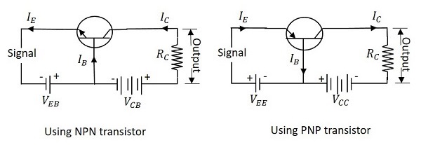
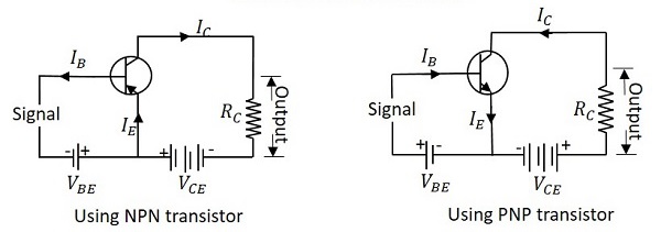
Transistor as an Amplifier
For a transistor to act as an amplifier, it should be properly biased. We will discuss the need for proper biasing in the next chapter. Here, let us focus how a transistor works as an amplifier.
Transistor Amplifier
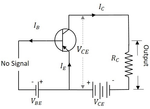
A transistor acts as an amplifier by raising the strength of a weak signal. The DC bias voltage applied to the emitter base junction, makes it remain in forward biased condition. This forward bias is maintained regardless of the polarity of the signal. The below figure shows how a transistor looks like when connected as an amplifier.
The low resistance in input circuit, lets any small change in input signal to result in an appreciable change in the output. The emitter current caused by the input signal contributes the collector current, which when flows through the load resistor RL, results in a large voltage drop across it. Thus a small input voltage results in a large output voltage, which shows that the transistor works as an amplifier.
Example
Let there be a change of 0.1v in the input voltage being applied, which further produces a change of 1mA in the emitter current. This emitter current will obviously produce a change in collector current, which would also be 1mA.
A load resistance of 5kΩ placed in the collector would produce a voltage of
5 kΩ × 1 mA = 5V
Hence it is observed that a change of 0.1v in the input gives a change of 5v in the output, which means the voltage level of the signal is amplified.
Performance of Amplifier
As the common emitter mode of connection is mostly adopted, let us first understand a few important terms with reference to this mode of connection.
Input Resistance
As the input circuit is forward biased, the input resistance will be low. The input resistance is the opposition offered by the base-emitter junction to the signal flow.
By definition, it is the ratio of small change in base-emitter voltage (ΔVBE) to the resulting change in base current (ΔIB) at constant collector-emitter voltage.
Input resistance, $R_i = \frac{\Delta V_{BE}}{\Delta I_B}$
Where Ri = input resistance, VBE = base-emitter voltage, and IB = base current.
Output Resistance
The output resistance of a transistor amplifier is very high. The collector current changes very slightly with the change in collector-emitter voltage.
By definition, it is the ratio of change in collector-emitter voltage (ΔVCE) to the resulting change in collector current (ΔIC) at constant base current.
Output resistance = $R_o = \frac{\Delta V_{CE}}{\Delta I_C}$
Where Ro = Output resistance, VCE = Collector-emitter voltage, and IC = Collector-emitter voltage.
Effective Collector Load
The load is connected at the collector of a transistor and for a single-stage amplifier, the output voltage is taken from the collector of the transistor and for a multi-stage amplifier, the same is collected from a cascaded stages of transistor circuit.
By definition, it is the total load as seen by the a.c. collector current. In case of single stage amplifiers, the effective collector load is a parallel combination of RC and Ro.
Effective Collector Load, $R_{AC} = R_C // R_o$
$$= \frac{R_C \times R_o}{R_C + R_o} = R_{AC}$$
Hence for a single stage amplifier, effective load is equal to collector load RC.
In a multi-stage amplifier (i.e. having more than one amplification stage), the input resistance Ri of the next stage also comes into picture.
Effective collector load becomes parallel combination of RC, Ro and Ri i.e,
Effective Collector Load, $R_{AC} = R_C // R_o // R_i$
$$R_C // R_i = \frac{R_C R_i}{R_C + R_i}$$
As input resistance Ri is quite small, therefore effective load is reduced.
Current Gain
The gain in terms of current when the changes in input and output currents are observed, is called as Current gain. By definition, it is the ratio of change in collector current (ΔIC) to the change in base current (ΔIB).
Current gain, $\beta = \frac{\Delta I_C}{\Delta I_B}$
The value of β ranges from 20 to 500. The current gain indicates that input current becomes β times in the collector current.
Voltage Gain
The gain in terms of voltage when the changes in input and output currents are observed, is called as Voltage gain. By definition, it is the ratio of change in output voltage (ΔVCE) to the change in input voltage (ΔVBE).
Voltage gain, $A_V = \frac{\Delta V_{CE}}{\Delta V_{BE}}$
$$= \frac{Change \: in\: output \: current \times effective\: load}{Change \: in\: input \: current \times input \: resistance}$$
$$= \frac{\Delta I_C \times R_{AC}}{\Delta I_B \times R_i} = \frac{\Delta I_C}{\Delta I_B} \times \frac{R_{AC}}{R_i} = \beta \times \frac{R_{AC}}{R_i}$$
For a single stage, RAC = RC.
However, for Multistage,
$$R_{AC} = \frac{R_C \times R_i}{R_C + R_i}$$
Where Ri is the input resistance of the next stage.
Power Gain
The gain in terms of power when the changes in input and output currents are observed, is called as Power gain.
By definition, it is the ratio of output signal power to the input signal power.
Power gain, $A_P = \frac{(\Delta I_C)^2 \times R_{AC}}{(\Delta I_B)^2 \times R_i}$
$$= \left ( \frac{\Delta I_C}{\Delta I_B} \right ) \times \frac{\Delta I_C \times R_{AC}}{\Delta I_B \times R_i}$$
= Current gain × Voltage gain
Hence these are all the important terms which refer the performance of amplifiers.
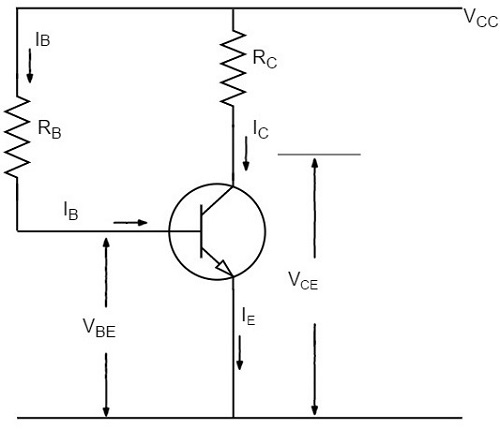
Transistor Biasing
Biasing is the process of providing DC voltage which helps in the functioning of the circuit. A transistor is based in order to make the emitter base junction forward biased and collector base junction reverse biased, so that it maintains in active region, to work as an amplifier.
In the previous chapter, we explained how a transistor acts as a good amplifier, if both the input and output sections are biased.
Transistor Biasing
The proper flow of zero signal collector current and the maintenance of proper collectoremitter voltage during the passage of signal is known as Transistor Biasing. The circuit which provides transistor biasing is called as Biasing Circuit.
Need for DC biasing
If a signal of very small voltage is given to the input of BJT, it cannot be amplified. Because, for a BJT, to amplify a signal, two conditions have to be met.
The input voltage should exceed cut-in voltage for the transistor to be ON.
The BJT should be in the active region, to be operated as an amplifier.
If appropriate DC voltages and currents are given through BJT by external sources, so that BJT operates in active region and superimpose the AC signals to be amplified, then this problem can be avoided. The given DC voltage and currents are so chosen that the transistor remains in active region for entire input AC cycle. Hence DC biasing is needed.
The below figure shows a transistor amplifier that is provided with DC biasing on both input and output circuits.

For a transistor to be operated as a faithful amplifier, the operating point should be stabilized. Let us have a look at the factors that affect the stabilization of operating point.
Factors affecting the operating point
The main factor that affect the operating point is the temperature. The operating point shifts due to change in temperature.
As temperature increases, the values of ICE, β, VBE gets affected.
- ICBO gets doubled (for every 10o rise)
- VBE decreases by 2.5mv (for every 1o rise)
So the main problem which affects the operating point is temperature. Hence operating point should be made independent of the temperature so as to achieve stability. To achieve this, biasing circuits are introduced.
Stabilization
The process of making the operating point independent of temperature changes or variations in transistor parameters is known as Stabilization.
Once the stabilization is achieved, the values of IC and VCE become independent of temperature variations or replacement of transistor. A good biasing circuit helps in the stabilization of operating point.
Need for Stabilization
Stabilization of the operating point has to be achieved due to the following reasons.
- Temperature dependence of IC
- Individual variations
- Thermal runaway
Let us understand these concepts in detail.
Temperature Dependence of IC
As the expression for collector current IC is
$$I_C = \beta I_B + I_{CEO}$$
$$= \beta I_B + (\beta + 1) I_{CBO}$$
The collector leakage current ICBO is greatly influenced by temperature variations. To come out of this, the biasing conditions are set so that zero signal collector current IC = 1 mA. Therefore, the operating point needs to be stabilized i.e. it is necessary to keep IC constant.
Individual Variations
As the value of β and the value of VBE are not same for every transistor, whenever a transistor is replaced, the operating point tends to change. Hence it is necessary to stabilize the operating point.
Thermal Runaway
As the expression for collector current IC is
$$I_C = \beta I_B + I_{CEO}$$
$$= \beta I_B + (\beta + 1)I_{CBO}$$
The flow of collector current and also the collector leakage current causes heat dissipation. If the operating point is not stabilized, there occurs a cumulative effect which increases this heat dissipation.
The self-destruction of such an unstabilized transistor is known as Thermal run away.
In order to avoid thermal runaway and the destruction of transistor, it is necessary to stabilize the operating point, i.e., to keep IC constant.
Stability Factor
It is understood that IC should be kept constant in spite of variations of ICBO or ICO. The extent to which a biasing circuit is successful in maintaining this is measured by Stability factor. It denoted by S.
By definition, the rate of change of collector current IC with respect to the collector leakage current ICO at constant β and IB is called Stability factor.
$S = \frac{d I_C}{d I_{CO}}$ at constant IB and β
Hence we can understand that any change in collector leakage current changes the collector current to a great extent. The stability factor should be as low as possible so that the collector current doesn’t get affected. S=1 is the ideal value.
The general expression of stability factor for a CE configuration can be obtained as under.
$$I_C = \beta I_B + (\beta + 1)I_{CO}$$
Differentiating above expression with respect to IC, we get
$$1 = \beta \frac{d I_B}{d I_C} + (\beta + 1)\frac{d I_{CO}}{dI_C}$$
Or
$$1 = \beta \frac{d I_B}{d I_C} + \frac{(\beta + 1)}{S}$$
Since $\frac{d I_{CO}}{d I_C} = \frac{1}{S}$
Or
$$S = \frac{\beta + 1}{1 - \beta \left (\frac{d I_B}{d I_C} \right )}$$
Hence the stability factor S depends on β, IB and IC.
Methods of Transistor Biasing
The biasing in transistor circuits is done by using two DC sources VBB and VCC. It is economical to minimize the DC source to one supply instead of two which also makes the circuit simple.
The commonly used methods of transistor biasing are
- Base Resistor method
- Collector to Base bias
- Biasing with Collector feedback resistor
- Voltage-divider bias
All of these methods have the same basic principle of obtaining the required value of IB and IC from VCC in the zero signal conditions.
Base Resistor Method
In this method, a resistor RB of high resistance is connected in base, as the name implies. The required zero signal base current is provided by VCC which flows through RB. The base emitter junction is forward biased, as base is positive with respect to emitter.
The required value of zero signal base current and hence the collector current (as IC = βIB) can be made to flow by selecting the proper value of base resistor RB. Hence the value of RB is to be known. The figure below shows how a base resistor method of biasing circuit looks like.
Let IC be the required zero signal collector current. Therefore,
$$I_B = \frac{I_C}{\beta}$$
Considering the closed circuit from VCC, base, emitter and ground, while applying the Kirchhoff’s voltage law, we get,
$$V_{CC} = I_B R_B + V_{BE}$$
Or
$$I_B R_B = V_{CC} - V_{BE}$$
Therefore
$$R_B = \frac{V_{CC} - V_{BE}}{I_B}$$
Since VBE is generally quite small as compared to VCC, the former can be neglected with little error. Then,
$$R_B = \frac{V_{CC}}{I_B}$$
We know that VCC is a fixed known quantity and IB is chosen at some suitable value. As RB can be found directly, this method is called as fixed bias method.
Stability factor
$$S = \frac{\beta + 1}{1 - \beta \left ( \frac{d I_B}{d I_C} \right )}$$
In fixed-bias method of biasing, IB is independent of IC so that,
$$\frac{d I_B}{d I_C} = 0$$
Substituting the above value in the previous equation,
Stability factor, $S = \beta + 1$
Thus the stability factor in a fixed bias is (β+1) which means that IC changes (β+1) times as much as any change in ICO.
Advantages
- The circuit is simple.
- Only one resistor RE is required.
- Biasing conditions are set easily.
- No loading effect as no resistor is present at base-emitter junction.
Disadvantages
The stabilization is poor as heat development can’t be stopped.
The stability factor is very high. So, there are strong chances of thermal run away.
Hence, this method is rarely employed.
Collector to Base Bias
The collector to base bias circuit is same as base bias circuit except that the base resistor RB is returned to collector, rather than to VCC supply as shown in the figure below.
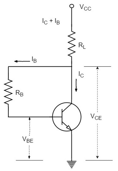
This circuit helps in improving the stability considerably. If the value of IC increases, the voltage across RL increases and hence the VCE also increases. This in turn reduces the base current IB. This action somewhat compensates the original increase.
The required value of RB needed to give the zero signal collector current IC can be calculated as follows.
Voltage drop across RL will be
$$R_L = (I_C + I_B)R_L \cong I_C R_L$$
From the figure,
$$I_C R_L + I_B R_B + V_{BE} = V_{CC}$$
Or
$$I_B R_B = V_{CC} - V_{BE} - I_C R_L$$
Therefore
$$R_B = \frac{V_{CC} - V_{BE} - I_C R_L}{I_B}$$
Or
$$R_B = \frac{(V_{CC} - V_{BE} - I_C R_L)\beta}{I_C}$$
Applying KVL we have
$$(I_B + I_C)R_L + I_B R_B + V_{BE} = V_{CC}$$
Or
$$I_B(R_L + R_B) + I_C R_L + V_{BE} = V_{CC}$$
Therefore
$$I_B = \frac{V_{CC} - V_{BE} - I_C R_L}{R_L + R_B}$$
Since VBE is almost independent of collector current, we get
$$\frac{d I_B}{d I_C} = - \frac{R_L}{R_L + R_B}$$
We know that
$$S = \frac{1 + \beta}{1 - \beta (d I_B / d I_C)}$$
Therefore
$$S = \frac{1 + \beta}{1 + \beta \left ( \frac{R_L}{R_L + R_B} \right )}$$
This value is smaller than (1+β) which is obtained for fixed bias circuit. Thus there is an improvement in the stability.
This circuit provides a negative feedback which reduces the gain of the amplifier. So the increased stability of the collector to base bias circuit is obtained at the cost of AC voltage gain.
Biasing with Collector Feedback resistor
In this method, the base resistor RB has its one end connected to base and the other to the collector as its name implies. In this circuit, the zero signal base current is determined by VCB but not by VCC.
It is clear that VCB forward biases the base-emitter junction and hence base current IB flows through RB. This causes the zero signal collector current to flow in the circuit. The below figure shows the biasing with collector feedback resistor circuit.
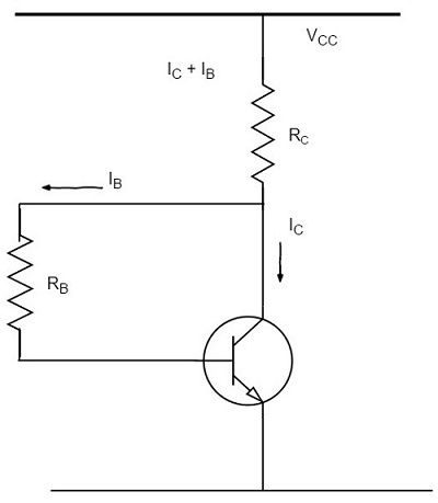
The required value of RB needed to give the zero signal current IC can be determined as follows.
$$V_{CC} = I_C R_C + I_B R_B + V_{BE}$$
Or
$$R_B = \frac{V_{CC} - V_{BE} - I_C R_C}{I_B}$$
$$= \frac{V_{CC} - V_{BE} - \beta I_B R_C}{I_B}$$
Since $I_C = \beta I_B$
Alternatively,
$$V_{CE} = V_{BE} + V_{CB}$$
Or
$$V_{CB} = V_{CE} - V_{BE}$$
Since
$$R_B = \frac{V_{CB}}{I_B} = \frac{V_{CE} - V_{BE}}{I_B}$$
Where
$$I_B = \frac{I_C}{\beta}$$
Mathematically,
Stability factor, $S < (\beta + 1)$
Therefore, this method provides better thermal stability than the fixed bias.
The Q-point values for the circuit are shown as
$$I_C = \frac{V_{CC} - V_{BE}}{R_B/ \beta + R_C}$$
$$V_{CE} = V_{CC} - I_C R_C$$
Advantages
- The circuit is simple as it needs only one resistor.
- This circuit provides some stabilization, for lesser changes.
Disadvantages
- The circuit doesn’t provide good stabilization.
- The circuit provides negative feedback.
Voltage Divider Bias Method
Among all the methods of providing biasing and stabilization, the voltage divider bias method is the most prominent one. Here, two resistors R1 and R2 are employed, which are connected to VCC and provide biasing. The resistor RE employed in the emitter provides stabilization.
The name voltage divider comes from the voltage divider formed by R1 and R2. The voltage drop across R2 forward biases the base-emitter junction. This causes the base current and hence collector current flow in the zero signal conditions. The figure below shows the circuit of voltage divider bias method.
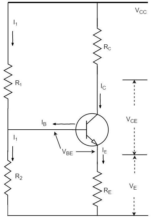
Suppose that the current flowing through resistance R1 is I1. As base current IB is very small, therefore, it can be assumed with reasonable accuracy that current flowing through R2 is also I1.
Now let us try to derive the expressions for collector current and collector voltage.
Collector Current, IC
From the circuit, it is evident that,
$$I_1 = \frac{V_{CC}}{R_1 + R_2}$$
Therefore, the voltage across resistance R2 is
$$V_2 = \left ( \frac{V_{CC}}{R_1 + R_2}\right ) R_2$$
Applying Kirchhoff’s voltage law to the base circuit,
$$V_2 = V_{BE} + V_E$$
$$V_2 = V_{BE} + I_E R_E$$
$$I_E = \frac{V_2 - V_{BE}}{R_E}$$
Since IE ≈ IC,
$$I_C = \frac{V_2 - V_{BE}}{R_E}$$
From the above expression, it is evident that IC doesn’t depend upon β. VBE is very small that IC doesn’t get affected by VBE at all. Thus IC in this circuit is almost independent of transistor parameters and hence good stabilization is achieved.
Collector-Emitter Voltage, VCE
Applying Kirchhoff’s voltage law to the collector side,
$$V_{CC} = I_C R_C + V_{CE} + I_E R_E$$
Since IE ≅ IC
$$= I_C R_C + V_{CE} + I_C R_E$$
$$= I_C(R_C + R_E) + V_{CE}$$
Therefore,
$$V_{CE} = V_{CC} - I_C(R_C + R_E)$$
RE provides excellent stabilization in this circuit.
$$V_2 = V_{BE} + I_C R_E$$
Suppose there is a rise in temperature, then the collector current IC decreases, which causes the voltage drop across RE to increase. As the voltage drop across R2 is V2, which is independent of IC, the value of VBE decreases. The reduced value of IB tends to restore IC to the original value.
Stability Factor
The equation for Stability factor of this circuit is obtained as
Stability Factor = $S = \frac{(\beta + 1) (R_0 + R_3)}{R_0 + R_E + \beta R_E}$
$$= (\beta + 1) \times \frac{1 + \frac{R_0}{R_E}}{\beta + 1 + \frac{R_0}{R_E}}$$
Where
$$R_0 = \frac{R_1 R_2}{R_1 + R_2}$$
If the ratio R0/RE is very small, then R0/RE can be neglected as compared to 1 and the stability factor becomes
Stability Factor = $S = (\beta + 1) \times \frac{1}{\beta + 1} = 1$
This is the smallest possible value of S and leads to the maximum possible thermal stability.
Bias Compensation
So far we have seen different stabilization techniques. The stabilization occurs due to negative feedback action. The negative feedback, although improves the stability of operating point, it reduces the gain of the amplifier.
As the gain of the amplifier is a very important consideration, some compensation techniques are used to maintain excellent bias and thermal stabilization. Let us now go through such bias compensation techniques.
Diode Compensation for Instability
These are the circuits that implement compensation techniques using diodes to deal with biasing instability. The stabilization techniques refer to the use of resistive biasing circuits which permit IB to vary so as to keep IC relatively constant.
There are two types of diode compensation methods. They are −
- Diode compensation for instability due to VBE variation
- Diode compensation for instability due to ICO variation
Let us understand these two compensation methods in detail.
Diode Compensation for Instability due to VBE Variation
In a Silicon transistor, the changes in the value of VBE results in the changes in IC. A diode can be employed in the emitter circuit in order to compensate the variations in VBE or ICO. As the diode and transistor used are of same material, the voltage VD across the diode has same temperature coefficient as VBE of the transistor.
The following figure shows self-bias with stabilization and compensation.
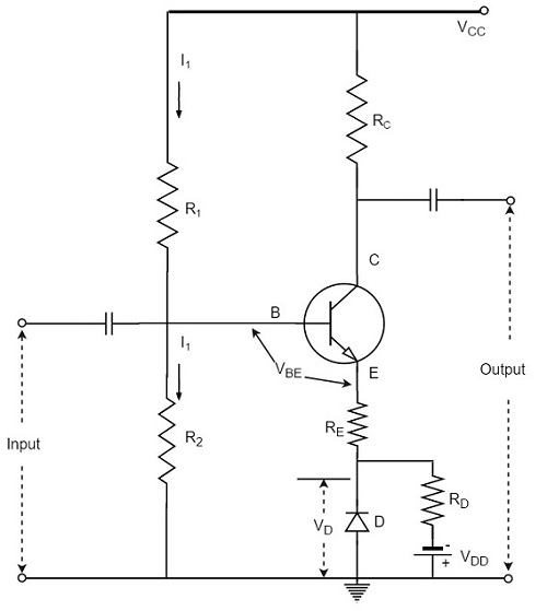
The diode D is forward biased by the source VDD and the resistor RD. The variation in VBE with temperature is same as the variation in VD with temperature, hence the quantity (VBE – VD) remains constant. So the current IC remains constant in spite of the variation in VBE.
Diode Compensation for Instability due to ICO Variation
The following figure shows the circuit diagram of a transistor amplifier with diode D used for compensation of variation in ICO.
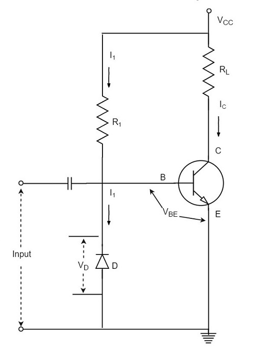
So, the reverse saturation current IO of the diode will increase with temperature at the same rate as the transistor collector saturation current ICO.
$$I = \frac{V_{CC} - V_{BE}}{R} \cong \frac{V_{CC}}{R} = Constant$$
The diode D is reverse biased by VBE and the current through it is the reverse saturation current IO.
Now the base current is,
$$I_B = I - I_O$$
Substituting the above value in the expression for collector current.
$$I_C = \beta (I - I_O) + (1 + \beta)I_{CO}$$
If β ≫ 1,
$$I_C = \beta I - \beta I_O + \beta I_{CO}$$
I is almost constant and if IO of diode and ICO of transistor track each other over the operating temperature range, then IC remains constant.
Other Compensations
There are other compensation techniques which refer to the use of temperature sensitive devices such as diodes, transistors, thermistors, Sensistors, etc. to compensate for the variation in currents.
There are two popular types of circuits in this method, one using a thermistor and the other using a Sensistor. Let us have a look at them.
Thermistor Compensation
Thermistor is a temperature sensitive device. It has negative temperature coefficient. The resistance of a thermistor increases when the temperature decreases and it decreases when the temperature increases. The below figure shows a self-bias amplifier with thermistor compensation.
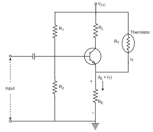
In an amplifier circuit, the changes that occur in ICO, VBE and β with temperature, increases the collector current. Thermistor is employed to minimize the increase in collector current. As the temperature increases, the resistance RT of thermistor decreases, which increases the current through it and the resistor RE. Now, the voltage developed across RE increases, which reverse biases the emitter junction. This reverse bias is so high that the effect of resistors R1 and R2 providing forward bias also gets reduced. This action reduces the rise in collector current.
Thus the temperature sensitivity of thermistor compensates the increase in collector current, occurred due to temperature.
Sensistor Compensation
A Sensistor is a heavily doped semiconductor that has positive temperature coefficient. The resistance of a Sensistor increases with the increase in temperature and decreases with the decrease in temperature. The figure below shows a self-bias amplifier with Sensistor compensation.
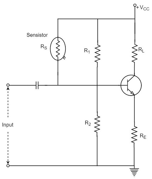
In the above figure, the Sensistor may be placed in parallel with R1 or in parallel with RE. As the temperature increases, the resistance of the parallel combination, thermistor and R1 increases and their voltage drop also increases. This decreases the voltage drop across R2. Due to the decrease of this voltage, the net forward emitter bias decreases. As a result of this, IC decreases.
Hence by employing the Sensistor, the rise in the collector current which is caused by the increase of ICO, VBE and β due to temperature, gets controlled.
Thermal Resistance
The transistor is a temperature dependent device. When the transistor is operated, the collector junction gets heavy flow of electrons and hence has much heat generated. This heat if increased further beyond the permissible limit, damages the junction and thus the transistor.
In order to protect itself from damage, the transistor dissipates heat from the junction to the transistor case and from there to the open air surrounding it.
Let, the ambient temperature or the temperature of surrounding air = TAoC
And, the temperature of collector-base junction of the transistor = TJoC
As TJ > TA, the difference TJ - TA is greater than the power dissipated in the transistor PD will be greater. Thus,
$$T_J - T_A \propto P_D$$
$$T_J - T_A = HP_D$$
Where H is the constant of proportionality, and is called as Thermal resistance.
Thermal resistance is the resistance to heat flow from junction to surrounding air. It is denoted by H.
$$H = \frac{T_J - T_A}{P_D}$$
The unit of H is oC/watt.
If the thermal resistance is low, the transfer of heat from the transistor into the air, will be easy. If the transistor case is larger, the heat dissipation will be better. This is achieved by the use of Heat sink.
Heat Sink
The transistor that handle larger powers, dissipates more heat during operation. This heat if not dissipated properly, could damage the transistor. Hence the power transistors are generally mounted on large metal cases to provide a larger area to get the heat radiated that is generated during its operation.
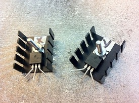
The metal sheet that helps to dissipate the additional heat from the transistor is known as the heat sink. The ability of a heat sink depends upon its material, volume, area, shape, contact between case and sink, and the movement of air around the sink.
The heat sink is selected after considering all these factors. The image shows a power transistor with a heat sink.
A tiny transistor in the above image is fixed to a larger metal sheet in order to dissipate its heat, so that the transistor doesn’t get damaged.
Thermal Runaway
The use of heat sink avoids the problem of Thermal Runaway. It is a situation where an increase in temperature leads to the condition that further increase in temperature, leads to the destruction of the device itself. This is a kind of uncontrollable positive feedback.
Heat sink is not the only consideration; other factors such as operating point, ambient temperature, and the type of transistor used can also cause thermal runaway.
Basic Amplifier
We hope that you have gained sufficient knowledge on operating point, its stability and the compensation techniques in the previous chapter. Let us now try to understand the fundamental concepts of a basic amplifier circuit.
An electronic signal contains some information which cannot be utilized if doesn’t have proper strength. The process of increasing the signal strength is called as Amplification. Almost all electronic equipment must include some means for amplifying the signals. We find the use of amplifiers in medical devices, scientific equipment, automation, military tools, communication devices, and even in household equipment.
Amplification in practical applications is done using Multi-stage amplifiers. A number of single-stage amplifiers are cascaded to form a Multi-stage amplifier. Let us see how a single-stage amplifier is built, which is the basic for a Multi-stage amplifier.
Single-stage Transistor Amplifier
When only one transistor with associated circuitry is used for amplifying a weak signal, the circuit is known as single-stage amplifier.
Analyzing the working of a Single-stage amplifier circuit, makes us easy to understand the formation and working of Multi-stage amplifier circuits. A Single stage transistor amplifier has one transistor, bias circuit and other auxiliary components. The following circuit diagram shows how a single stage transistor amplifier looks like.
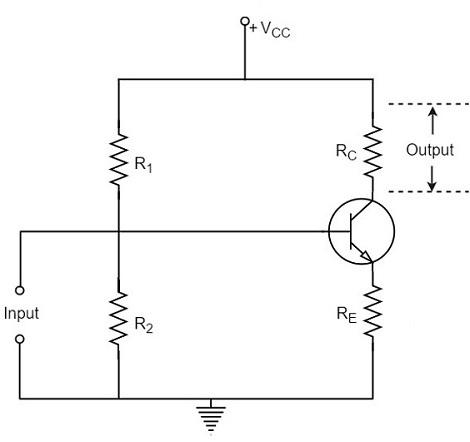
When a weak input signal is given to the base of the transistor as shown in the figure, a small amount of base current flows. Due to the transistor action, a larger current flows in the collector of the transistor. (As the collector current is β times of the base current which means IC = βIB). Now, as the collector current increases, the voltage drop across the resistor RC also increases, which is collected as the output.
Hence a small input at the base gets amplified as the signal of larger magnitude and strength at the collector output. Hence this transistor acts as an amplifier.
Practical Circuit of a Transistor Amplifier
The circuit of a practical transistor amplifier is as shown below, which represents a voltage divider biasing circuit.
The various prominent circuit elements and their functions are as described below.
Biasing Circuit
The resistors R1, R2 and RE form the biasing and stabilization circuit, which helps in establishing a proper operating point.
Input Capacitor Cin
This capacitor couples the input signal to the base of the transistor. The input capacitor Cin allows AC signal, but isolates the signal source from R2. If this capacitor is not present, the input signal gets directly applied, which changes the bias at R2.
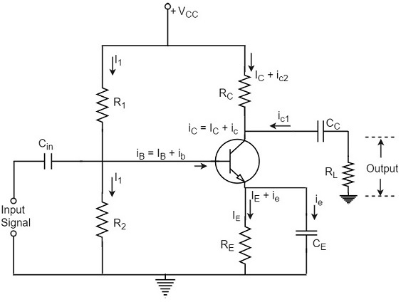
Coupling Capacitor CC
This capacitor is present at the end of one stage and connects it to the other stage. As it couples two stages it is called as coupling capacitor. This capacitor blocks DC of one stage to enter the other but allows AC to pass. Hence it is also called as blocking capacitor.
Due to the presence of coupling capacitor CC, the output across the resistor RL is free from the collector’s DC voltage. If this is not present, the bias conditions of the next stage will be drastically changed due to the shunting effect of RC, as it would come in parallel to R2 of the next stage.
Emitter by-pass capacitor CE
This capacitor is employed in parallel to the emitter resistor RE. The amplified AC signal is by passed through this. If this is not present, that signal will pass through RE which produces a voltage drop across RE that will feedback the input signal reducing the output voltage.
The Load resistor RL
The resistance RL connected at the output is known as Load resistor. When a number of stages are used, then RL represents the input resistance of the next stage.
Various Circuit currents
Let us go through various circuit currents in the complete amplifier circuit. These are already mentioned in the above figure.
Base Current
When no signal is applied in the base circuit, DC base current IB flows due to biasing circuit. When AC signal is applied, AC base current ib also flows. Therefore, with the application of signal, total base current iB is given by
$$i_B = I_B + i_b$$
Collector Current
When no signal is applied, a DC collector current IC flows due to biasing circuit. When AC signal is applied, AC collector current ic also flows. Therefore, the total collector current iC is given by
$$i_C = I_C + i_c$$
Where
$I_C = \beta I_B$ = zero signal collecor current
$i_c = \beta i_b$ = collecor current due to signal
Emitter Current
When no signal is applied, a DC emitter current IE flows. With the application of signal, total emitter current iE is given by
$$i_E = I_E + i_e$$
It should be remembered that
$$I_E = I_B + I_C$$
$$i_e = i_b + i_c$$
As base current is usually small, it is to be noted that
$I_E \cong I_C$ and $i_e \cong i_c$
These are the important considerations for the practical circuit of transistor amplifier. Now let us know about the classification of Amplifiers.
Amplifiers Classification
An Amplifier circuit is one which strengthens the signal. The amplifier action and the important considerations for the practical circuit of transistor amplifier were also detailed in previous chapters.
Let us now try to understand the classification of amplifiers. Amplifiers are classified according to many considerations.
Based on number of stages
Depending upon the number of stages of Amplification, there are Single-stage amplifiers and Multi-stage amplifiers.
Single-stage Amplifiers − This has only one transistor circuit, which is a singlestage amplification.
Multi-stage Amplifiers − This has multiple transistor circuit, which provides multi-stage amplification.
Based on its output
Depending upon the parameter that is amplified at the output, there are voltage and power amplifiers.
Voltage Amplifiers − The amplifier circuit that increases the voltage level of the input signal, is called as Voltage amplifier.
Power Amplifiers − The amplifier circuit that increases the power level of the input signal, is called as Power amplifier.
Based on the input signals
Depending upon the magnitude of the input signal applied, they can be categorized as Small signal and large signal amplifiers.
Small signal Amplifiers − When the input signal is so weak so as to produce small fluctuations in the collector current compared to its quiescent value, the amplifier is known as Small signal amplifier.
Large signal amplifiers − When the fluctuations in collector current are large i.e. beyond the linear portion of the characteristics, the amplifier is known as large signal amplifier.
Based on the frequency range
Depending upon the frequency range of the signals being used, there are audio and radio amplifiers.
Audio Amplifiers − The amplifier circuit that amplifies the signals that lie in the audio frequency range i.e. from 20Hz to 20 KHz frequency range, is called as audio amplifier.
Power Amplifiers − The amplifier circuit that amplifies the signals that lie in a very high frequency range, is called as Power amplifier.
Based on Biasing Conditions
Depending upon their mode of operation, there are class A, class B and class C amplifiers.
Class A amplifier − The biasing conditions in class A power amplifier are such that the collector current flows for the entire AC signal applied.
Class B amplifier − The biasing conditions in class B power amplifier are such that the collector current flows for half-cycle of input AC signal applied.
Class C amplifier − The biasing conditions in class C power amplifier are such that the collector current flows for less than half cycle of input AC signal applied.
Class AB amplifier − The class AB power amplifier is one which is created by combining both class A and class B in order to have all the advantages of both the classes and to minimize the problems they have.
Based on the Coupling method
Depending upon the method of coupling one stage to the other, there are RC coupled, Transformer coupled and direct coupled amplifier.
RC Coupled amplifier − A Multi-stage amplifier circuit that is coupled to the next stage using resistor and capacitor (RC) combination can be called as a RC coupled amplifier.
Transformer Coupled amplifier − A Multi-stage amplifier circuit that is coupled to the next stage, with the help of a transformer, can be called as a Transformer coupled amplifier.
Direct Coupled amplifier − A Multi-stage amplifier circuit that is coupled to the next stage directly, can be called as a direct coupled amplifier.
Based on the Transistor Configuration
Depending upon the type of transistor configuration, there are CE CB and CC amplifiers.
CE amplifier − The amplifier circuit that is formed using a CE configured transistor combination is called as CE amplifier.
CB amplifier − The amplifier circuit that is formed using a CB configured transistor combination is called as CB amplifier.
CC amplifier − The amplifier circuit that is formed using a CC configured transistor combination is called as CC amplifier.
Based on Configurations
Any transistor amplifier, uses a transistor to amplify the signals which is connected in one of the three configurations. For an amplifier it is a better state to have a high input impedance, in order to avoid loading effect in Multi-stage circuits and lower output impedance, in order to deliver maximum output to the load. The voltage gain and power gain should also be high to produce a better output.
Let us now study different configurations to understand which configuration suits better for a transistor to work as an amplifier.
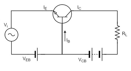
CB Amplifier
The amplifier circuit that is formed using a CB configured transistor combination is called as CB amplifier.
Construction
The common base amplifier circuit using NPN transistor is as shown below, the input signal being applied at emitter base junction and the output signal being taken from collector base junction.
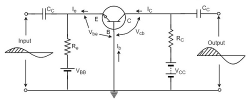
The emitter base junction is forward biased by VEE and collector base junction is reverse biased by VCC. The operating point is adjusted with the help of resistors Re and Rc. Thus the values of Ic, Ib and Icb are decided by VCC, VEE, Re and Rc.
Operation
When no input is applied, the quiescent conditions are formed and no output is present. As Vbe is at negative with respect to ground, the forward bias is decreased, for the positive half of the input signal. As a result of this, the base current IB also gets decreased.
The below figure shows the CB amplifier with self-bias circuit.
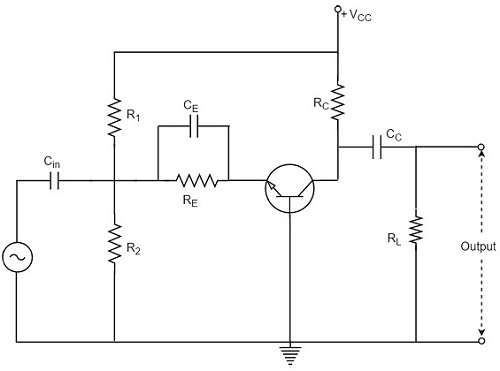
As we know that,
$$I_C \cong I_E \cong \beta I_B$$
Both the collector current and emitter current get decreased.
The voltage drop across RC is
$$V_C = I_C R_C$$
This VC also gets decreased.
As ICRC decreases, VCB increases. It is because,
$$V_{CB} = V_{CC} - I_C R_C$$
Thus, a positive half cycle output is produced.
In CB configuration, a positive input produces a positive output and hence input and output are in phase. So, there is no phase reversal between input and output in a CB amplifier.
If CB configuration is considered for amplification, it has low input impedance and high output impedance. The voltage gain is also low compared to CE configuration. Hence CB configured amplifiers are used at high frequency applications.
CE Amplifier
The amplifier circuit that is formed using a CE configured transistor combination is called as CE amplifier.
Construction
The common emitter amplifier circuit using NPN transistor is as shown below, the input signal being applied at emitter base junction and the output signal being taken from collector base junction.
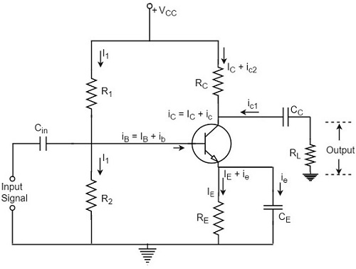
The emitter base junction is forward biased by VEE and collector base junction is reverse biased by VCC. The operating point is adjusted with the help of resistors Re and Rc. Thus the values of Ic, Ib and Icb are decided by VCC, VEE, Re and Rc.
Operation
When no input is applied, the quiescent conditions are formed and no output is present. When positive half of the signal is being applied, the voltage between base and emitter Vbe is increased because it is already positive with respect to ground.
As forward bias increases, the base current too increases accordingly. Since IC = βIB, the collector current increases as well.
The following circuit diagram shows a CE amplifier with self-bias circuit.
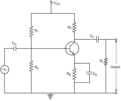
The collector current when flows through RC, the voltage drop increases.
$$V_C = I_C R_C$$
As a consequence of this, the voltage between collector and emitter decreases. Because,
$$V_{CB} = V_{CC} - I_C R_C$$
Thus, the amplified voltage appears across RC.
Therefore, in a CE amplifier, as the positive going signal appears as a negative going signal, it is understood that there is a phase shift of 180o between input and output.
CE amplifier has a high input impedance and lower output impedance than CB amplifier. The voltage gain and power gain are also high in CE amplifier and hence this is mostly used in Audio amplifiers.
CC Amplifier
The amplifier circuit that is formed using a CC configured transistor combination is called as CC amplifier.
Construction
The common collector amplifier circuit using NPN transistor is as shown below, the input signal being applied at base collector junction and the output signal being taken from emitter collector junction.
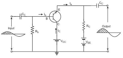
The emitter base junction is forward biased by VEE and collector base junction is reverse biased by VCC. The Q-values of Ib and Ie are adjusted by Rb and Re.
Operation
When no input is applied, the quiescent conditions are formed and no output is present. When positive half of the signal is being applied, the forward bias is increased because Vbe is positive with respect to collector or ground. With this, the base current IB and the collector current IC are increased.
The following circuit diagram shows a CC amplifier with self-bias circuit.
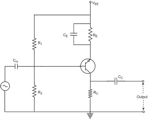
Consequently, the voltage drop across Re i.e. the output voltage is increased. As a result, positive half cycle is obtained. As the input and output are in phase, there is no phase reversal.
If CC configuration is considered for amplification, though CC amplifier has better input impedance and lower output impedance than CE amplifier, the voltage gain of CC is very less which limits its applications to impedance matching only.
Comparison between CB CE CC Amplifiers
Let us compare the characteristic details of CB, CE, and CC amplifiers.
| Characteristic | CE | CB | CC |
|---|---|---|---|
| Input resistance | Low (1K to 2K) | Very low (30-150 Ω) | High (20-500 KΩ) |
| Output resistance | Large (≈ 50 K) | High (≈ 500 K) | Low (50-1000 KΩ) |
| Current gain | B high | α < 1 | High (1 + β) |
| Voltage gain | High (≈ 1500) | High (≈ 1500) | Less than one |
| Power gain | High (≈ 10,000) | High (≈ 7500) | Low (250-500) |
| Phase between input and output | reversed | same | same |
Due to the compatibility and characteristic features, the common-emitter configuration is mostly used in amplifier circuits.
Multi-Stage Transistor Amplifier
In practical applications, the output of a single state amplifier is usually insufficient, though it is a voltage or power amplifier. Hence they are replaced by Multi-stage transistor amplifiers.
In Multi-stage amplifiers, the output of first stage is coupled to the input of next stage using a coupling device. These coupling devices can usually be a capacitor or a transformer. This process of joining two amplifier stages using a coupling device can be called as Cascading.
The following figure shows a two-stage amplifier connected in cascade.
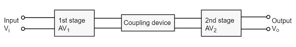
The overall gain is the product of voltage gain of individual stages.
$$A_V = A_{V1} \times A_{V2} = \frac{V_2}{V_1} \times \frac{V_0}{V_2} = \frac{V_0}{V_1}$$
Where AV = Overall gain, AV1 = Voltage gain of 1st stage, and AV2 = Voltage gain of 2nd stage.
If there are n number of stages, the product of voltage gains of those n stages will be the overall gain of that multistage amplifier circuit.
Purpose of coupling device
The basic purposes of a coupling device are
To transfer the AC from the output of one stage to the input of next stage.
To block the DC to pass from the output of one stage to the input of next stage, which means to isolate the DC conditions.
Types of Coupling
Joining one amplifier stage with the other in cascade, using coupling devices form a Multi-stage amplifier circuit. There are four basic methods of coupling, using these coupling devices such as resistors, capacitors, transformers etc. Let us have an idea about them.
Resistance-Capacitance Coupling
This is the mostly used method of coupling, formed using simple resistor-capacitor combination. The capacitor which allows AC and blocks DC is the main coupling element used here.
The coupling capacitor passes the AC from the output of one stage to the input of its next stage. While blocking the DC components from DC bias voltages to effect the next stage. Let us get into the details of this method of coupling in the coming chapters.
Impedance Coupling
The coupling network that uses inductance and capacitance as coupling elements can be called as Impedance coupling network.
In this impedance coupling method, the impedance of coupling coil depends on its inductance and signal frequency which is jwL. This method is not so popular and is seldom employed.
Transformer Coupling
The coupling method that uses a transformer as the coupling device can be called as Transformer coupling. There is no capacitor used in this method of coupling because the transformer itself conveys the AC component directly to the base of second stage.
The secondary winding of the transformer provides a base return path and hence there is no need of base resistance. This coupling is popular for its efficiency and its impedance matching and hence it is mostly used.
Direct Coupling
If the previous amplifier stage is connected to the next amplifier stage directly, it is called as direct coupling. The individual amplifier stage bias conditions are so designed that the stages can be directly connected without DC isolation.
The direct coupling method is mostly used when the load is connected in series, with the output terminal of the active circuit element. For example, head-phones, loud speakers etc.
Role of Capacitors in Amplifiers
Other than the coupling purpose, there are other purposes for which few capacitors are especially employed in amplifiers. To understand this, let us know about the role of capacitors in Amplifiers.
The Input Capacitor Cin
The input capacitor Cin present at the initial stage of the amplifier, couples AC signal to the base of the transistor. This capacitor Cin if not present, the signal source will be in parallel to resistor R2 and the bias voltage of the transistor base will be changed.
Hence Cin allows, the AC signal from source to flow into input circuit, without affecting the bias conditions.
The Emitter By-pass Capacitor Ce
The emitter by-pass capacitor Ce is connected in parallel to the emitter resistor. It offers a low reactance path to the amplified AC signal.
In the absence of this capacitor, the voltage developed across RE will feedback to the input side thereby reducing the output voltage. Thus in the presence of Ce the amplified AC will pass through this.
Coupling Capacitor CC
The capacitor CC is the coupling capacitor that connects two stages and prevents DC interference between the stages and controls the operating point from shifting. This is also called as blocking capacitor because it does not allow the DC voltage to pass through it.
In the absence of this capacitor, RC will come in parallel with the resistance R1 of the biasing network of the next stage and thereby changing the biasing conditions of the next stage.
Amplifier Consideration
For an amplifier circuit, the overall gain of the amplifier is an important consideration. To achieve maximum voltage gain, let us find the most suitable transistor configuration for cascading.
CC Amplifier
- Its voltage gain is less than unity.
- It is not suitable for intermediate stages.
CB Amplifier
- Its voltage gain is less than unity.
- Hence not suitable for cascading.
CE Amplifier
- Its voltage gain is greater than unity.
- Voltage gain is further increased by cascading.
The characteristics of CE amplifier are such that, this configuration is very suitable for cascading in amplifier circuits. Hence most of the amplifier circuits use CE configuration.
In the subsequent chapters of this tutorial, we will explain the types of coupling amplifiers.
RC Coupling Amplifier
The resistance-capacitance coupling is, in short termed as RC coupling. This is the mostly used coupling technique in amplifiers.
Construction of a Two-stage RC Coupled Amplifier
The constructional details of a two-stage RC coupled transistor amplifier circuit are as follows. The two stage amplifier circuit has two transistors, connected in CE configuration and a common power supply VCC is used. The potential divider network R1 and R2 and the resistor Re form the biasing and stabilization network. The emitter by-pass capacitor Ce offers a low reactance path to the signal.
The resistor RL is used as a load impedance. The input capacitor Cin present at the initial stage of the amplifier couples AC signal to the base of the transistor. The capacitor CC is the coupling capacitor that connects two stages and prevents DC interference between the stages and controls the shift of operating point. The figure below shows the circuit diagram of RC coupled amplifier.
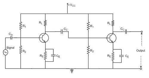
Operation of RC Coupled Amplifier
When an AC input signal is applied to the base of first transistor, it gets amplified and appears at the collector load RL which is then passed through the coupling capacitor CC to the next stage. This becomes the input of the next stage, whose amplified output again appears across its collector load. Thus the signal is amplified in stage by stage action.
The important point that has to be noted here is that the total gain is less than the product of the gains of individual stages. This is because when a second stage is made to follow the first stage, the effective load resistance of the first stage is reduced due to the shunting effect of the input resistance of the second stage. Hence, in a multistage amplifier, only the gain of the last stage remains unchanged.
As we consider a two stage amplifier here, the output phase is same as input. Because the phase reversal is done two times by the two stage CE configured amplifier circuit.
Frequency Response of RC Coupled Amplifier
Frequency response curve is a graph that indicates the relationship between voltage gain and function of frequency. The frequency response of a RC coupled amplifier is as shown in the following graph.
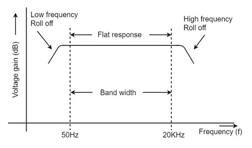
From the above graph, it is understood that the frequency rolls off or decreases for the frequencies below 50Hz and for the frequencies above 20 KHz. whereas the voltage gain for the range of frequencies between 50Hz and 20 KHz is constant.
We know that,
$$X_C = \frac{1}{2 \pi f_c}$$
It means that the capacitive reactance is inversely proportional to the frequency.
At Low frequencies (i.e. below 50 Hz)
The capacitive reactance is inversely proportional to the frequency. At low frequencies, the reactance is quite high. The reactance of input capacitor Cin and the coupling capacitor CC are so high that only small part of the input signal is allowed. The reactance of the emitter by pass capacitor CE is also very high during low frequencies. Hence it cannot shunt the emitter resistance effectively. With all these factors, the voltage gain rolls off at low frequencies.
At High frequencies (i.e. above 20 KHz)
Again considering the same point, we know that the capacitive reactance is low at high frequencies. So, a capacitor behaves as a short circuit, at high frequencies. As a result of this, the loading effect of the next stage increases, which reduces the voltage gain. Along with this, as the capacitance of emitter diode decreases, it increases the base current of the transistor due to which the current gain (β) reduces. Hence the voltage gain rolls off at high frequencies.
At Mid-frequencies (i.e. 50 Hz to 20 KHz)
The voltage gain of the capacitors is maintained constant in this range of frequencies, as shown in figure. If the frequency increases, the reactance of the capacitor CC decreases which tends to increase the gain. But this lower capacitance reactive increases the loading effect of the next stage by which there is a reduction in gain.
Due to these two factors, the gain is maintained constant.
Advantages of RC Coupled Amplifier
The following are the advantages of RC coupled amplifier.
The frequency response of RC amplifier provides constant gain over a wide frequency range, hence most suitable for audio applications.
The circuit is simple and has lower cost because it employs resistors and capacitors which are cheap.
It becomes more compact with the upgrading technology.
Disadvantages of RC Coupled Amplifier
The following are the disadvantages of RC coupled amplifier.
The voltage and power gain are low because of the effective load resistance.
They become noisy with age.
Due to poor impedance matching, power transfer will be low.
Applications of RC Coupled Amplifier
The following are the applications of RC coupled amplifier.
They have excellent audio fidelity over a wide range of frequency.
Widely used as Voltage amplifiers
Due to poor impedance matching, RC coupling is rarely used in the final stages.
Transformer Coupled Amplifier
We have observed that the main drawback of RC coupled amplifier is that the effective load resistance gets reduced. This is because, the input impedance of an amplifier is low, while its output impedance is high.
When they are coupled to make a multistage amplifier, the high output impedance of one stage comes in parallel with the low input impedance of next stage. Hence, effective load resistance is decreased. This problem can be overcome by a transformer coupled amplifier.
In a transformer-coupled amplifier, the stages of amplifier are coupled using a transformer. Let us go into the constructional and operational details of a transformer coupled amplifier.
Construction of Transformer Coupled Amplifier
The amplifier circuit in which, the previous stage is connected to the next stage using a coupling transformer, is called as Transformer coupled amplifier.
The coupling transformer T1 is used to feed the output of 1st stage to the input of 2nd stage. The collector load is replaced by the primary winding of the transformer. The secondary winding is connected between the potential divider and the base of 2nd stage, which provides the input to the 2nd stage. Instead of coupling capacitor like in RC coupled amplifier, a transformer is used for coupling any two stages, in the transformer coupled amplifier circuit.
The figure below shows the circuit diagram of transformer coupled amplifier.
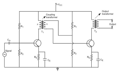
The potential divider network R1 and R2 and the resistor Re together form the biasing and stabilization network. The emitter by-pass capacitor Ce offers a low reactance path to the signal. The resistor RL is used as a load impedance. The input capacitor Cin present at the initial stage of the amplifier couples AC signal to the base of the transistor. The capacitor CC is the coupling capacitor that connects two stages and prevents DC interference between the stages and controls the shift of operating point.
Operation of Transformer Coupled Amplifier
When an AC signal is applied to the input of the base of the first transistor then it gets amplified by the transistor and appears at the collector to which the primary of the transformer is connected.
The transformer which is used as a coupling device in this circuit has the property of impedance changing, which means the low resistance of a stage (or load) can be reflected as a high load resistance to the previous stage. Hence the voltage at the primary is transferred according to the turns ratio of the secondary winding of the transformer.
This transformer coupling provides good impedance matching between the stages of amplifier. The transformer coupled amplifier is generally used for power amplification.
Frequency Response of Transformer Coupled Amplifier
The figure below shows the frequency response of a transformer coupled amplifier. The gain of the amplifier is constant only for a small range of frequencies. The output voltage is equal to the collector current multiplied by the reactance of primary.
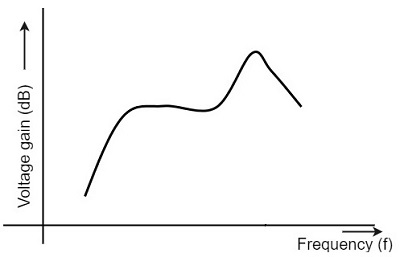
At low frequencies, the reactance of primary begins to fall, resulting in decreased gain. At high frequencies, the capacitance between turns of windings acts as a bypass condenser to reduce the output voltage and hence gain.
So, the amplification of audio signals will not be proportionate and some distortion will also get introduced, which is called as Frequency distortion.
Advantages of Transformer Coupled Amplifier
The following are the advantages of a transformer coupled amplifier −
- An excellent impedance matching is provided.
- Gain achieved is higher.
- There will be no power loss in collector and base resistors.
- Efficient in operation.
Disadvantages of Transformer Coupled Amplifier
The following are the disadvantages of a transformer coupled amplifier −
Though the gain is high, it varies considerably with frequency. Hence a poor frequency response.
Frequency distortion is higher.
Transformers tend to produce hum noise.
Transformers are bulky and costly.
Applications
The following are the applications of a transformer coupled amplifier −
- Mostly used for impedance matching purposes.
- Used for Power amplification.
- Used in applications where maximum power transfer is needed.
Direct Coupled Amplifier
The other type of coupling amplifier is the direct coupled amplifier, which is especially used to amplify lower frequencies, such as amplifying photo-electric current or thermo-couple current or so.
Direct Coupled Amplifier
As no coupling devices are used, the coupling of the amplifier stages is done directly and hence called as Direct coupled amplifier.
Construction
The figure below indicates the three stage direct coupled transistor amplifier. The output of first stage transistor T1 is connected to the input of second stage transistor T2.
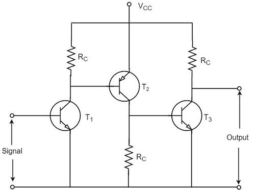
The transistor in the first stage will be an NPN transistor, while the transistor in the next stage will be a PNP transistor and so on. This is because, the variations in one transistor tend to cancel the variations in the other. The rise in the collector current and the variation in β of one transistor gets cancelled by the decrease in the other.
Operation
The input signal when applied at the base of transistor T1, it gets amplified due to the transistor action and the amplified output appears at the collector resistor Rc of transistor T1. This output is applied to the base of transistor T2 which further amplifies the signal. In this way, a signal is amplified in a direct coupled amplifier circuit.
Advantages
The advantages of direct coupled amplifier are as follows.
The circuit arrangement is simple because of minimum use of resistors.
The circuit is of low cost because of the absence of expensive coupling devices.
Disadvantages
The disadvantages of direct coupled amplifier are as follows.
- It cannot be used for amplifying high frequencies.
- The operating point is shifted due to temperature variations.
Applications
The applications of direct coupled amplifier are as follows.
- Low frequency amplifications.
- Low current amplifications.
Comparisions
Let us try to compare the characteristics of different types of coupling methods discussed till now.
| S.No | Particular | RC Coupling | Transformer Coupling | Direct Coupling |
|---|---|---|---|---|
| 1 | Frequency response | Excellent in audio frequency range | Poor | Best |
| 2 | Cost | Less | More | Least |
| 3 | Space and Weight | Less | More | Least |
| 4 | Impedance matching | Not good | Excellent | Good |
| 5 | Use | For voltage amplification | For Power amplification | For amplifying extremely low frequencies |
Power Amplifiers
In practice, any amplifier consists of few stages of amplification. If we consider audio amplification, it has several stages of amplification, depending upon our requirement.
Power Amplifier
After the audio signal is converted into electrical signal, it has several voltage amplifications done, after which the power amplification of the amplified signal is done just before the loud speaker stage. This is clearly shown in the below figure.
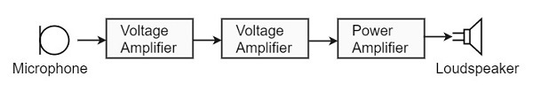
While the voltage amplifier raises the voltage level of the signal, the power amplifier raises the power level of the signal. Besides raising the power level, it can also be said that a power amplifier is a device which converts DC power to AC power and whose action is controlled by the input signal.
The DC power is distributed according to the relation,
DC power input = AC power output + losses
Power Transistor
For such Power amplification, a normal transistor would not do. A transistor that is manufactured to suit the purpose of power amplification is called as a Power transistor.
A Power transistor differs from the other transistors, in the following factors.
It is larger in size, in order to handle large powers.
The collector region of the transistor is made large and a heat sink is placed at the collector-base junction in order to minimize heat generated.
The emitter and base regions of a power transistor are heavily doped.
Due to the low input resistance, it requires low input power.
Hence there is a lot of difference in voltage amplification and power amplification. So, let us now try to get into the details to understand the differences between a voltage amplifier and a power amplifier.
Difference between Voltage and Power Amplifiers
Let us try to differentiate between voltage and power amplifier.
Voltage Amplifier
The function of a voltage amplifier is to raise the voltage level of the signal. A voltage amplifier is designed to achieve maximum voltage amplification.
The voltage gain of an amplifier is given by
$$A_v = \beta \left (\frac{R_c}{R_{in}} \right )$$
The characteristics of a voltage amplifier are as follows −
The base of the transistor should be thin and hence the value of β should be greater than 100.
The resistance of the input resistor Rin should be low when compared to collector load RC.
The collector load RC should be relatively high. To permit high collector load, the voltage amplifiers are always operated at low collector current.
The voltage amplifiers are used for small signal voltages.
Power Amplifier
The function of a power amplifier is to raise the power level of input signal. It is required to deliver a large amount of power and has to handle large current.
The characteristics of a power amplifier are as follows −
The base of transistor is made thicken to handle large currents. The value of β being (β > 100) high.
The size of the transistor is made larger, in order to dissipate more heat, which is produced during transistor operation.
Transformer coupling is used for impedance matching.
Collector resistance is made low.
The comparison between voltage and power amplifiers is given below in a tabular form.
| S.No | Particular | Voltage Amplifier | Power Amplifier |
|---|---|---|---|
| 1 | β | High (>100) | Low (5 to 20) |
| 2 | RC | High (4-10 KΩ) | Low (5 to 20 Ω) |
| 3 | Coupling | Usually R-C coupling | Invariably transformer coupling |
| 4 | Input voltage | Low (a few m V) | High (2-4 V) |
| 5 | Collector current | Low (≈ 1 mA) | High (> 100 mA) |
| 6 | Power output | Low | High |
| 7 | Output impendence | High (≈ 12 K Ω) | Low (200 Ω) |
Classification of Power Amplifiers
The Power amplifiers amplify the power level of the signal. This amplification is done in the last stage in audio applications. The applications related to radio frequencies employ radio power amplifiers. But the operating point of a transistor, plays a very important role in determining the efficiency of the amplifier. The main classification is done based on this mode of operation.
The classification is done based on their frequencies and also based on their mode of operation.
Classification Based on Frequencies
Power amplifiers are divided into two categories, based on the frequencies they handle. They are as follows.
Audio Power Amplifiers − The audio power amplifiers raise the power level of signals that have audio frequency range (20 Hz to 20 KHz). They are also known as Small signal power amplifiers.
Radio Power Amplifiers − Radio Power Amplifiers or tuned power amplifiers raise the power level of signals that have radio frequency range (3 KHz to 300 GHz). They are also known as large signal power amplifiers.
Classification Based on Mode of Operation
On the basis of the mode of operation, i.e., the portion of the input cycle during which collector current flows, the power amplifiers may be classified as follows.
Class A Power amplifier − When the collector current flows at all times during the full cycle of signal, the power amplifier is known as class A power amplifier.
Class B Power amplifier − When the collector current flows only during the positive half cycle of the input signal, the power amplifier is known as class B power amplifier.
Class C Power amplifier − When the collector current flows for less than half cycle of the input signal, the power amplifier is known as class C power amplifier.
There forms another amplifier called Class AB amplifier, if we combine the class A and class B amplifiers so as to utilize the advantages of both.
Before going into the details of these amplifiers, let us have a look at the important terms that have to be considered to determine the efficiency of an amplifier.
Terms Considering Performance
The primary objective of a power amplifier is to obtain maximum output power. In order to achieve this, the important factors to be considered are collector efficiency, power dissipation capability and distortion. Let us go through them in detail.
Collector Efficiency
This explains how well an amplifier converts DC power to AC power. When the DC supply is given by the battery but no AC signal input is given, the collector output at such a condition is observed as collector efficiency.
The collector efficiency is defined as
$$\eta = \frac{average\: a.c \: power \: output}{average \: d.c \: power\: input\: to \: transistor}$$
For example, if the battery supplies 15W and AC output power is 3W. Then the transistor efficiency will be 20%.
The main aim of a power amplifier is to obtain maximum collector efficiency. Hence the higher the value of collector efficiency, the efficient the amplifier will be.
Power Dissipation Capacity
Every transistor gets heated up during its operation. As a power transistor handles large currents, it gets more heated up. This heat increases the temperature of the transistor, which alters the operating point of the transistor.
So, in order to maintain the operating point stability, the temperature of the transistor has to be kept in permissible limits. For this, the heat produced has to be dissipated. Such a capacity is called as Power dissipation capability.
Power dissipation capability can be defined as the ability of a power transistor to dissipate the heat developed in it. Metal cases called heat sinks are used in order to dissipate the heat produced in power transistors.
Distortion
A transistor is a non-linear device. When compared with the input, there occur few variations in the output. In voltage amplifiers, this problem is not pre-dominant as small currents are used. But in power amplifiers, as large currents are in use, the problem of distortion certainly arises.
Distortion is defined as the change of output wave shape from the input wave shape of the amplifier. An amplifier that has lesser distortion, produces a better output and hence considered efficient.
Class A Power Amplifiers
We have already come across the details of transistor biasing, which is very important for the operation of a transistor as an amplifier. Hence to achieve faithful amplification, the biasing of the transistor has to be done such that the amplifier operates over the linear region.
A Class A power amplifier is one in which the output current flows for the entire cycle of the AC input supply. Hence the complete signal present at the input is amplified at the output. The following figure shows the circuit diagram for Class A Power amplifier.
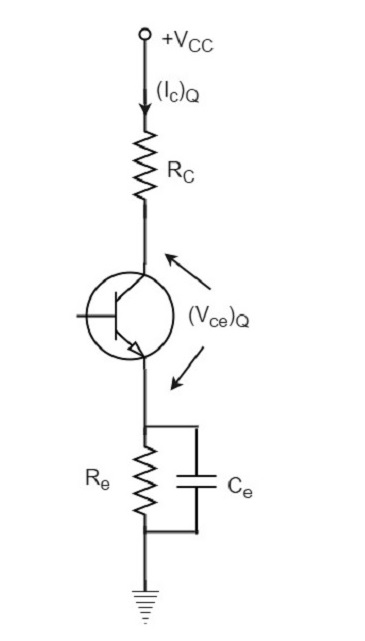
From the above figure, it can be observed that the transformer is present at the collector as a load. The use of transformer permits the impedance matching, resulting in the transference of maximum power to the load e.g. loud speaker.
The operating point of this amplifier is present in the linear region. It is so selected that the current flows for the entire ac input cycle. The below figure explains the selection of operating point.
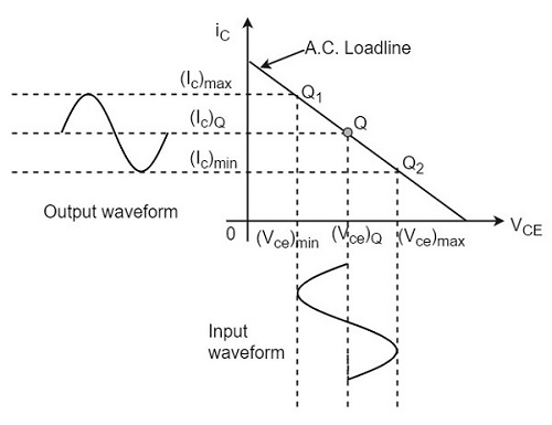
The output characteristics with operating point Q is shown in the figure above. Here (Ic)Q and (Vce)Q represent no signal collector current and voltage between collector and emitter respectively. When signal is applied, the Q-point shifts to Q1 and Q2. The output current increases to (Ic)max and decreases to (Ic)min. Similarly, the collector-emitter voltage increases to (Vce)max and decreases to (Vce)min.
D.C. Power drawn from collector battery Vcc is given by
$$P_{in} = voltage \times current = V_{CC}(I_C)_Q$$
This power is used in the following two parts −
- Power dissipated in the collector load as heat is given by
$$P_{RC} = (current)^2 \times resistance = (I_C)^2_Q R_C$$
- Power given to transistor is given by
$$P_{tr} = P_{in} - P_{RC} = V_{CC} - (I_C)^2_Q R_C$$
When signal is applied, the power given to transistor is used in the following two parts −
A.C. Power developed across load resistors RC which constitutes the a.c. power output.
$$(P_O)_{ac} = I^2 R_C = \frac{V^2}{R_C} = \left ( \frac{V_m}{\sqrt{2}}\right )^2 \frac{1}{R_C} = \frac{V_m^2}{2R_C}$$
Where I is the R.M.S. value of a.c. output current through load, V is the R.M.S. value of a.c. voltage, and Vm is the maximum value of V.
The D.C. power dissipated by the transistor (collector region) in the form of heat, i.e., (PC)dc
We have represented the whole power flow in the following diagram.
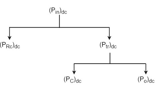
This class A power amplifier can amplify small signals with least distortion and the output will be an exact replica of the input with increased strength.
Let us now try to draw some expressions to represent efficiencies.
Overall Efficiency
The overall efficiency of the amplifier circuit is given by
$$(\eta)_{overall} = \frac{a.c \: power \:delivered\: to \: the\: load}{total \: power\: delivered \: by \: d.c\: supply}$$
$$= \frac{(P_O)_{ac}}{(P_{in})_{dc}}$$
Collector Efficiency
The collector efficiency of the transistor is defined as
$$(\eta)_{collector} = \frac{average\: a.c \: power \:output}{average \:d.c\: power\: input\: to\: transistor}$$
$$= \frac{(P_O)_{ac}}{(P_{tr})_{dc}}$$
Expression for overall efficiency
$$(P_O)_{ac} = V_{rms} \times I_{rms}$$
$$= \frac{1}{\sqrt{2}} \left [ \frac{(V_{ce})_{max} - (V_{ce})_{min}}{2} \right ] \times \frac{1}{\sqrt{2}} \left [ \frac{(I_C)_{max} - (I_C)_{min}}{2}\right ]$$
$$= \frac{[(V_{ce})_{max} - (V_{ce})_{min}] \times [(I_C)_{max} - (I_C)_{min}]}{8}$$
Therefore
$$(\eta)_{overall} = \frac{[(V_{ce})_{max} - (V_{ce})_{min}] \times [(I_C)_{max} - (I_C)_{min}]}{8 \times V_{CC} (I_C)_Q}$$
Advantages of Class A Amplifiers
The advantages of Class A power amplifier are as follows −
- The current flows for complete input cycle
- It can amplify small signals
- The output is same as input
- No distortion is present
Disadvantages of Class A Amplifiers
The advantages of Class A power amplifier are as follows −
- Low power output
- Low collector efficiency
Transformer Coupled Class A Power Amplifier
The class A power amplifier as discussed in the previous chapter, is the circuit in which the output current flows for the entire cycle of the AC input supply. We also have learnt about the disadvantages it has such as low output power and efficiency. In order to minimize those effects, the transformer coupled class A power amplifier has been introduced.
The construction of class A power amplifier can be understood with the help of below figure. This is similar to the normal amplifier circuit but connected with a transformer in the collector load.
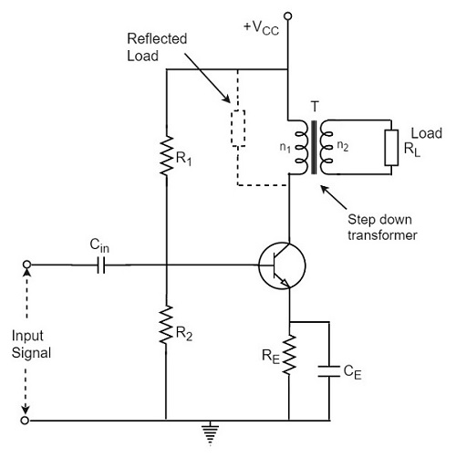
Here R1 and R2 provide potential divider arrangement. The resistor Re provides stabilization, Ce is the bypass capacitor and Re to prevent a.c. voltage. The transformer used here is a step-down transformer.
The high impedance primary of the transformer is connected to the high impedance collector circuit. The low impedance secondary is connected to the load (generally loud speaker).
Transformer Action
The transformer used in the collector circuit is for impedance matching. RL is the load connected in the secondary of a transformer. RL’ is the reflected load in the primary of the transformer.
The number of turns in the primary are n1 and the secondary are n2. Let V1 and V2 be the primary and secondary voltages and I1 and I2 be the primary and secondary currents respectively. The below figure shows the transformer clearly.
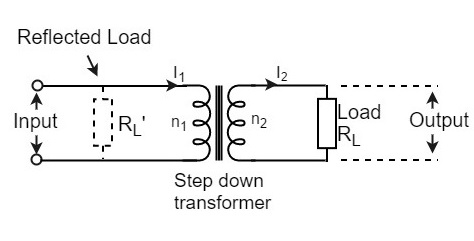
We know that
$$\frac{V_1}{V_2} = \frac{n_1}{n_2}\: and\: \frac{I_1}{I_2} = \frac{n_1}{n_2}$$
Or
$$V_1 = \frac{n_1}{n_2}V_2 \: and\: I_1 = \frac{n_1}{n_2}I_2$$
Hence
$$\frac{V_1}{I_1} = \left ( \frac{n_1}{n_2} \right )^2 \frac{V_2}{I_2}$$
But V1/I1 = RL’ = effective input resistance
And V2/I2 = RL = effective output resistance
Therefore,
$$R_L’ = \left ( \frac{n_1}{n_2}\right )^2 R_L = n^2 R_L$$
Where
$$n = \frac{number \: of \: turns \: in \: primary}{number\: of\: turns\: in\: secondary} = \frac{n_1}{n_2}$$
A power amplifier may be matched by taking proper turn ratio in step down transformer.
Circuit Operation
If the peak value of the collector current due to signal is equal to zero signal collector current, then the maximum a.c. power output is obtained. So, in order to achieve complete amplification, the operating point should lie at the center of the load line.
The operating point obviously varies when the signal is applied. The collector voltage varies in opposite phase to the collector current. The variation of collector voltage appears across the primary of the transformer.
Circuit Analysis
The power loss in the primary is assumed to be negligible, as its resistance is very small.
The input power under dc condition will be
$$(P_{in})_{dc} = (P_{tr})_{dc} = V_{CC} \times (I_C)_Q$$
Under maximum capacity of class A amplifier, voltage swings from (Vce)max to zero and current from (Ic)max to zero.
Hence
$$V_{rms} = \frac{1}{\sqrt{2}} \left [\frac{(V_{ce})_{max} - (V_{ce})_{min}}{2} \right ] = \frac{1}{\sqrt{2}} \left[ \frac{(V_{ce})_{max}}{2}\right ] = \frac{2V_{CC}}{2\sqrt{2}} = \frac{V_{CC}}{\sqrt{2}}$$
$$I_{rms} = \frac{1}{\sqrt{2}} \left [\frac{(I_C)_{max} - (I_C)_{min}}{2} \right ] = \frac{1}{\sqrt{2}} \left[ \frac{(I_C)_{max}}{2}\right ] = \frac{2(I_C)_Q}{2\sqrt{2}} = \frac{(I_C)_Q}{\sqrt{2}}$$
Therefore,
$$(P_O)_{ac} = V_{rms} \times I_{rms} = \frac{V_{CC}}{\sqrt{2}} \times \frac{(I_C)_Q}{\sqrt{2}} = \frac{V_{CC} \times (I_C)_Q}{2}$$
Therefore,
Collector Efficiency = $\frac{(P_O)_{ac}}{(P_{tr})_{dc}}$
Or,
$$(\eta)_{collector} = \frac{V_{CC} \times (I_C)_Q}{2 \times V_{CC} \times (I_C)_Q} = \frac{1}{2}$$
$$= \frac{1}{2} \times 100 = 50\%$$
The efficiency of a class A power amplifier is nearly than 30% whereas it has got improved to 50% by using the transformer coupled class A power amplifier.
Advantages
The advantages of transformer coupled class A power amplifier are as follows.
- No loss of signal power in the base or collector resistors.
- Excellent impedance matching is achieved.
- Gain is high.
- DC isolation is provided.
Disadvantages
The disadvantages of transformer coupled class A power amplifier are as follows.
- Low frequency signals are less amplified comparatively.
- Hum noise is introduced by transformers.
- Transformers are bulky and costly.
- Poor frequency response.
Applications
The applications of transformer coupled class A power amplifier are as follows.
This circuit is where impedance matching is the main criterion.
These are used as driver amplifiers and sometimes as output amplifiers.
Push-Pull Class A Power Amplifier
So far, we have seen two types of class A power amplifiers. The main problems that should be dealt with are low power output and efficiency. It is possible to obtain greater power output and efficiency than that of the Class A amplifier by using a combinational transistor pair called as Push-Pull configuration.
In this circuit, we use two complementary transistors in the output stage with one transistor being an NPN or N-channel type while the other transistor is a PNP or P-channel (the complement) type connected in order to operate them like PUSH a transistor to ON and PULL another transistor to OFF at the same time. This push-pull configuration can be made in class A, class B, class C or class AB amplifiers.
Construction of Push-Pull Class A Power Amplifier
The construction of the class A power amplifier circuit in push-pull configuration is shown as in the figure below. This arrangement mainly reduces the harmonic distortion introduced by the non-linearity of the transfer characteristics of a single transistor amplifier.
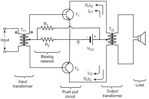
In Push-pull arrangement, the two identical transistors T1 and T2 have their emitter terminals shorted. The input signal is applied to the transistors through the transformer Tr1 which provides opposite polarity signals to both the transistor bases. The collectors of both the transistors are connected to the primary of output transformer Tr2. Both the transformers are center tapped. The VCC supply is provided to the collectors of both the transistors through the primary of the output transformer.
The resistors R1 and R2 provide the biasing arrangement. The load is generally a loudspeaker which is connected across the secondary of the output transformer. The turns ratio of the output transformer is chosen in such a way that the load is well matched with the output impedance of the transistor. So maximum power is delivered to the load by the amplifier.
Circuit Operation
The output is collected from the output transformer Tr2. The primary of this transformer Tr2 has practically no dc component through it. The transistors T1 and T2 have their collectors connected to the primary of transformer Tr2 so that their currents are equal in magnitude and flow in opposite directions through the primary of transformer Tr2.
When the a.c. input signal is applied, the base of transistor T1 is more positive while the base of transistor T2 is less positive. Hence the collector current ic1 of transistor T1 increases while the collector current ic2 of transistor T2 decreases. These currents flow in opposite directions in two halves of the primary of output transformer. Moreover, the flux produced by these currents will also be in opposite directions.
Hence, the voltage across the load will be induced voltage whose magnitude will be proportional to the difference of collector currents i.e.
$$(i_{c1} - i_{c2})$$
Similarly, for the negative input signal, the collector current ic2 will be more than ic1. In this case, the voltage developed across the load will again be due to the difference
$$(i_{c1} - i_{c2})$$
As $i_{c2} > i_{c1}$
The polarity of voltage induced across load will be reversed.
$$i_{c1} - i_{c2} = i_{c1} + (-i_{c2})$$
To have a better understanding, let us consider the below figure.
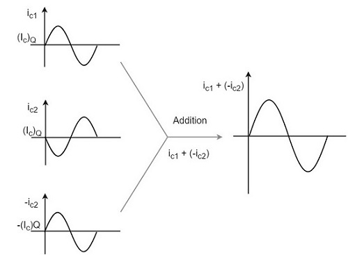
The overall operation results in an a.c. voltage induced in the secondary of output transformer and hence a.c. power is delivered to that load.
It is understood that, during any given half cycle of input signal, one transistor is being driven (or pushed) deep into conduction while the other being non-conducting (pulled out). Hence the name Push-pull amplifier. The harmonic distortion in Push-pull amplifier is minimized such that all the even harmonics are eliminated.
Advantages
The advantages of class A Push-pull amplifier are as follows
High a.c. output is obtained.
The output is free from even harmonics.
The effect of ripple voltages are balanced out. These are present in the power supply due to inadequate filtering.
Disadvantages
The disadvantages of class A Push-pull amplifier are as follows
- The transistors are to be identical, to produce equal amplification.
- Center-tapping is required for the transformers.
- The transformers are bulky and costly.
Class B Power Amplifier
When the collector current flows only during the positive half cycle of the input signal, the power amplifier is known as class B power amplifier.
Class B Operation
The biasing of the transistor in class B operation is in such a way that at zero signal condition, there will be no collector current. The operating point is selected to be at collector cut off voltage. So, when the signal is applied, only the positive half cycle is amplified at the output.
The figure below shows the input and output waveforms during class B operation.
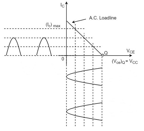
When the signal is applied, the circuit is forward biased for the positive half cycle of the input and hence the collector current flows. But during the negative half cycle of the input, the circuit is reverse biased and the collector current will be absent. Hence only the positive half cycle is amplified at the output.
As the negative half cycle is completely absent, the signal distortion will be high. Also, when the applied signal increases, the power dissipation will be more. But when compared to class A power amplifier, the output efficiency is increased.
Well, in order to minimize the disadvantages and achieve low distortion, high efficiency and high output power, the push-pull configuration is used in this class B amplifier.
Class B Push-Pull Amplifier
Though the efficiency of class B power amplifier is higher than class A, as only one half cycle of the input is used, the distortion is high. Also, the input power is not completely utilized. In order to compensate these problems, the push-pull configuration is introduced in class B amplifier.
Construction
The circuit of a push-pull class B power amplifier consists of two identical transistors T1 and T2 whose bases are connected to the secondary of the center-tapped input transformer Tr1. The emitters are shorted and the collectors are given the VCC supply through the primary of the output transformer Tr2.
The circuit arrangement of class B push-pull amplifier, is same as that of class A push-pull amplifier except that the transistors are biased at cut off, instead of using the biasing resistors. The figure below gives the detailing of the construction of a push-pull class B power amplifier.
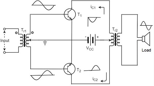
The circuit operation of class B push pull amplifier is detailed below.
Operation
The circuit of class B push-pull amplifier shown in the above figure clears that both the transformers are center-tapped. When no signal is applied at the input, the transistors T1 and T2 are in cut off condition and hence no collector currents flow. As no current is drawn from VCC, no power is wasted.
When input signal is given, it is applied to the input transformer Tr1 which splits the signal into two signals that are 180o out of phase with each other. These two signals are given to the two identical transistors T1 and T2. For the positive half cycle, the base of the transistor T1 becomes positive and collector current flows. At the same time, the transistor T2 has negative half cycle, which throws the transistor T2 into cutoff condition and hence no collector current flows. The waveform is produced as shown in the following figure.
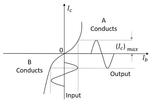
For the next half cycle, the transistor T1 gets into cut off condition and the transistor T2 gets into conduction, to contribute the output. Hence for both the cycles, each transistor conducts alternately. The output transformer Tr3 serves to join the two currents producing an almost undistorted output waveform.
Power Efficiency of Class B Push-Pull Amplifier
The current in each transistor is the average value of half sine loop.
For half sine loop, Idc is given by
$$I_{dc} = \frac{(I_C)_{max}}{\pi}$$
Therefore,
$$(p_{in})_{dc} = 2 \times \left [ \frac{(I_C)_{max}}{\pi} \times V_{CC} \right ]$$
Here factor 2 is introduced as there are two transistors in push-pull amplifier.
R.M.S. value of collector current = $(I_C)_{max}/ \sqrt{2}$
R.M.S. value of output voltage = $V_{CC} / \sqrt{2}$
Under ideal conditions of maximum power
Therefore,
$$(P_O)_{ac} = \frac{(I_C)_{max}}{\sqrt{2}} \times \frac{V_{CC}}{\sqrt{2}} = \frac{(I_C)_{max} \times V_{CC}}{2}$$
Now overall maximum efficiency
$$\eta_{overall} = \frac{(P_O)_{ac}}{(P_{in})_{dc}}$$
$$= \frac{(I_C)_{max} \times V_{CC}}{2} \times \frac{\pi}{2 (I_C)_{max} \times V_{CC}}$$
$$= \frac{\pi}{4} = 0.785 = 78.5\%$$
The collector efficiency would be the same.
Hence the class B push-pull amplifier improves the efficiency than the class A push-pull amplifier.
Complementary Symmetry Push-Pull Class B Amplifier
The push pull amplifier which was just discussed improves efficiency but the usage of center-tapped transformers makes the circuit bulky, heavy and costly. To make the circuit simple and to improve the efficiency, the transistors used can be complemented, as shown in the following circuit diagram.
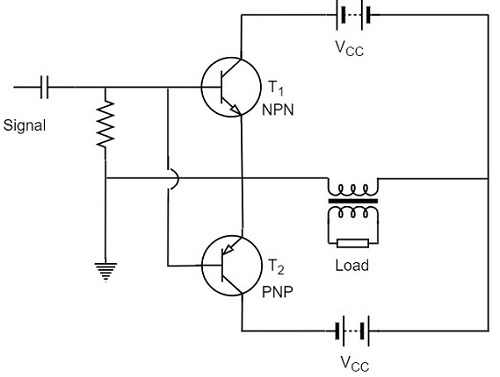
The above circuit employs a NPN transistor and a PNP transistor connected in push pull configuration. When the input signal is applied, during the positive half cycle of the input signal, the NPN transistor conducts and the PNP transistor cuts off. During the negative half cycle, the NPN transistor cuts off and the PNP transistor conducts.
In this way, the NPN transistor amplifies during positive half cycle of the input, while PNP transistor amplifies during negative half cycle of the input. As the transistors are both complement to each other, yet act symmetrically while being connected in push pull configuration of class B, this circuit is termed as Complementary symmetry push pull class B amplifier.
Advantages
The advantages of Complementary symmetry push pull class B amplifier are as follows.
As there is no need of center tapped transformers, the weight and cost are reduced.
Equal and opposite input signal voltages are not required.
Disadvantages
The disadvantages of Complementary symmetry push pull class B amplifier are as follows.
It is difficult to get a pair of transistors (NPN and PNP) that have similar characteristics.
We require both positive and negative supply voltages.
Class AB and Class C Power Amplifiers
The class A and class B amplifier so far discussed has got few limitations. Let us now try to combine these two to get a new circuit which would have all the advantages of both class A and class B amplifier without their inefficiencies. Before that, let us also go through another important problem, called as Cross over distortion, the output of class B encounters with.
Cross-over Distortion
In the push-pull configuration, the two identical transistors get into conduction, one after the other and the output produced will be the combination of both.
When the signal changes or crosses over from one transistor to the other at the zero voltage point, it produces an amount of distortion to the output wave shape. For a transistor in order to conduct, the base emitter junction should cross 0.7v, the cut off voltage. The time taken for a transistor to get ON from OFF or to get OFF from ON state is called the transition period.
At the zero voltage point, the transition period of switching over the transistors from one to the other, has its effect which leads to the instances where both the transistors are OFF at a time. Such instances can be called as Flat spot or Dead band on the output wave shape.
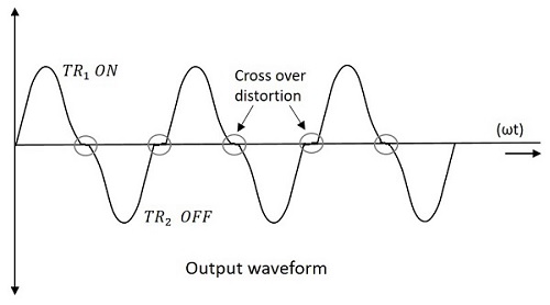
The above figure clearly shows the cross over distortion which is prominent in the output waveform. This is the main disadvantage. This cross over distortion effect also reduces the overall peak to peak value of the output waveform which in turn reduces the maximum power output. This can be more clearly understood through the non-linear characteristic of the waveform as shown below.
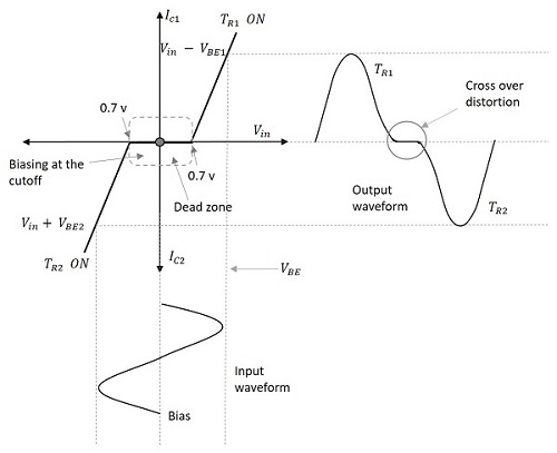
It is understood that this cross-over distortion is less pronounced for large input signals, where as it causes severe disturbance for small input signals. This cross over distortion can be eliminated if the conduction of the amplifier is more than one half cycle, so that both the transistors won’t be OFF at the same time.
This idea leads to the invention of class AB amplifier, which is the combination of both class A and class B amplifiers, as discussed below.
Class AB Power Amplifier
As the name implies, class AB is a combination of class A and class B type of amplifiers. As class A has the problem of low efficiency and class B has distortion problem, this class AB is emerged to eliminate these two problems, by utilizing the advantages of both the classes.
The cross over distortion is the problem that occurs when both the transistors are OFF at the same instant, during the transition period. In order to eliminate this, the condition has to be chosen for more than one half cycle. Hence, the other transistor gets into conduction, before the operating transistor switches to cut off state. This is achieved only by using class AB configuration, as shown in the following circuit diagram.
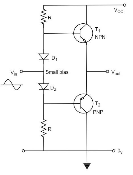
Therefore, in class AB amplifier design, each of the push-pull transistors is conducting for slightly more than the half cycle of conduction in class B, but much less than the full cycle of conduction of class A.
The conduction angle of class AB amplifier is somewhere between 180o to 360o depending upon the operating point selected. This is understood with the help of below figure.
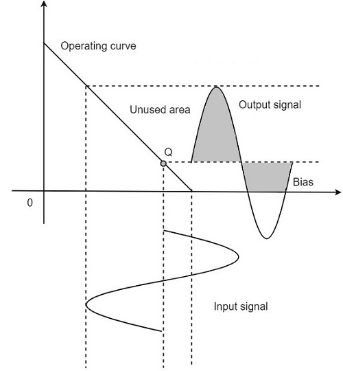
The small bias voltage given using diodes D1 and D2, as shown in the above figure, helps the operating point to be above the cutoff point. Hence the output waveform of class AB results as seen in the above figure. The crossover distortion created by class B is overcome by this class AB, as well the inefficiencies of class A and B don’t affect the circuit.
So, the class AB is a good compromise between class A and class B in terms of efficiency and linearity having the efficiency reaching about 50% to 60%. The class A, B and AB amplifiers are called as linear amplifiers because the output signal amplitude and phase are linearly related to the input signal amplitude and phase.
Class C Power Amplifier
When the collector current flows for less than half cycle of the input signal, the power amplifier is known as class C power amplifier.
The efficiency of class C amplifier is high while linearity is poor. The conduction angle for class C is less than 180o. It is generally around 90o, which means the transistor remains idle for more than half of the input signal. So, the output current will be delivered for less time compared to the application of input signal.
The following figure shows the operating point and output of a class C amplifier.
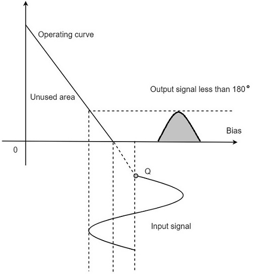
This kind of biasing gives a much improved efficiency of around 80% to the amplifier, but introduces heavy distortion in the output signal. Using the class C amplifier, the pulses produced at its output can be converted to complete sine wave of a particular frequency by using LC circuits in its collector circuit.
Tuned Amplifiers
The types of amplifiers that we have discussed so far cannot work effectively at radio frequencies, even though they are good at audio frequencies. Also, the gain of these amplifiers is such that it will not vary according to the frequency of the signal, over a wide range. This allows the amplification of the signal equally well over a range of frequencies and does not permit the selection of particular desired frequency while rejecting the other frequencies.
So, there occurs a need for a circuit which can select as well as amplify. So, an amplifier circuit along with a selection, such as a tuned circuit makes a Tuned amplifier.
What is a Tuned Amplifier?
Tuned amplifiers are the amplifiers that are employed for the purpose of tuning. Tuning means selecting. Among a set of frequencies available, if there occurs a need to select a particular frequency, while rejecting all other frequencies, such a process is called Selection. This selection is done by using a circuit called as Tuned circuit.
When an amplifier circuit has its load replaced by a tuned circuit, such an amplifier can be called as a Tuned amplifier circuit. The basic tuned amplifier circuit looks as shown below.
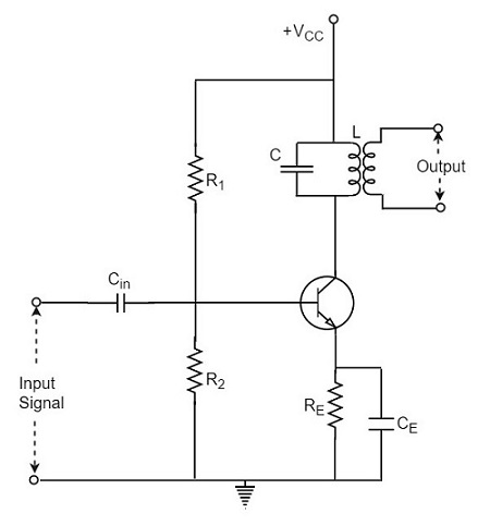
The tuner circuit is nothing but a LC circuit which is also called as resonant or tank circuit. It selects the frequency. A tuned circuit is capable of amplifying a signal over a narrow band of frequencies that are centered at resonant frequency.
When the reactance of the inductor balances the reactance of the capacitor, in the tuned circuit at some frequency, such a frequency can be called as resonant frequency. It is denoted by fr.
The formula for resonance is
$$2 \pi f_L = \frac{1}{2 \pi f_c}$$
$$f_r = \frac{1}{2 \pi \sqrt{LC}}$$
Types of Tuned Circuits
A tuned circuit can be Series tuned circuit (Series resonant circuit) or Parallel tuned circuit (parallel resonant circuit) according to the type of its connection to the main circuit.
Series Tuned Circuit
The inductor and capacitor connected in series make a series tuned circuit, as shown in the following circuit diagram.
At resonant frequency, a series resonant circuit offers low impedance which allows high current through it. A series resonant circuit offers increasingly high impedance to the frequencies far from the resonant frequency.
Parallel Tuned Circuit
The inductor and capacitor connected in parallel make a parallel tuned circuit, as shown in the below figure.
At resonant frequency, a parallel resonant circuit offers high impedance which does not allow high current through it. A parallel resonant circuit offers increasingly low impedance to the frequencies far from the resonant frequency.
Characteristics of a Parallel Tuned Circuit
The frequency at which parallel resonance occurs (i.e. reactive component of circuit current becomes zero) is called the resonant frequency fr. The main characteristics of a tuned circuit are as follows.
Impedance
The ratio of supply voltage to the line current is the impedance of the tuned circuit. Impedance offered by LC circuit is given by
$$\frac{Supply \: voltage}{Line equation} = \frac{V}{I}$$
At resonance, the line current increases while the impedance decreases.
The below figure represents the impedance curve of a parallel resonance circuit.
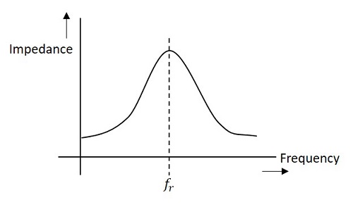
Impedance of the circuit decreases for the values above and below the resonant frequency fr. Hence the selection of a particular frequency and rejection of other frequencies is possible.
To obtain an equation for the circuit impedance, let us consider
Line Current $I = I_L cos \phi$
$$\frac{V}{Z_r} = \frac{V}{Z_L} \times \frac{R}{Z_L}$$
$$\frac{1}{Z_r} = \frac{R}{Z_L^2}$$
$$\frac{1}{Z_r} = \frac{R}{L/C} = \frac{C R}{L}$$
Since, $Z_L^2 = \frac{L}{C}$
Therefore, circuit impedance Zr is obtained as
$$Z_R = \frac{L}{C R}$$
Thus at parallel resonance, the circuit impedance is equal to L/CR.
Circuit Current
At parallel resonance, the circuit or line current I is given by the applied voltage divided by the circuit impedance Zr i.e.,
Line Current $I = \frac{V}{Z_r}$
Where $Z_r = \frac{L}{C R}$
Because Zr is very high, the line current I will be very small.
Quality Factor
For a parallel resonance circuit, the sharpness of the resonance curve determines the selectivity. The smaller the resistance of the coil, the sharper the resonant curve will be. Hence the inductive reactance and resistance of the coil determine the quality of the tuned circuit.
The ratio of inductive reactance of the coil at resonance to its resistance is known as Quality factor. It is denoted by Q.
$$Q = \frac{X_L}{R} = \frac{2 \pi f_r L}{R}$$
The higher the value of Q, the sharper the resonance curve and the better the selectivity will be.
Advantages of Tuned Amplifiers
The following are the advantages of tuned amplifiers.
The usage of reactive components like L and C, minimizes the power loss, which makes the tuned amplifiers efficient.
The selectivity and amplification of desired frequency is high, by providing higher impedance at resonant frequency.
A smaller collector supply VCC would do, because of its little resistance in parallel tuned circuit.
It is important to remember that these advantages are not applicable when there is a high resistive collector load.
Frequency Response of Tuned Amplifier
For an amplifier to be efficient, its gain should be high. This voltage gain depends upon β, input impedance and collector load. The collector load in a tuned amplifier is a tuned circuit.
The voltage gain of such an amplifier is given by
Voltage gain = $\frac{\beta Z_C}{Z_{in}}$
Where ZC = effective collector load and Zin = input impedance of the amplifier.
The value of ZC depends upon the frequency of the tuned amplifier. As ZC is maximum at resonant frequency, the gain of the amplifier is maximum at this resonant frequency.
Bandwidth
The range of frequencies at which the voltage gain of the tuned amplifier falls to 70.7% of the maximum gain is called its Bandwidth.
The range of frequencies between f1 and f2 is called as bandwidth of the tuned amplifier. The bandwidth of a tuned amplifier depends upon the Q of the LC circuit i.e., upon the sharpness of the frequency response. The value of Q and the bandwidth are inversely proportional.
The figure below details the bandwidth and frequency response of the tuned amplifier.
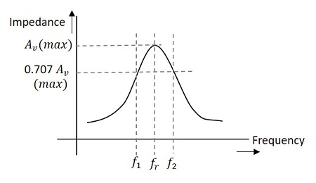
Relation between Q and Bandwidth
The quality factor Q of the bandwidth is defined as the ratio of resonant frequency to bandwidth, i.e.,
$$Q = \frac{f_r}{BW}$$
In general, a practical circuit has its Q value greater than 10.
Under this condition, the resonant frequency at parallel resonance is given by
$$f_r = \frac{1}{2 \pi \sqrt{LC}}$$
Types of Tuned Amplifiers
There are two main types of tuned amplifiers. They are −
- Single tuned amplifier
- Double tuned amplifier
Single Tuned Amplifier
An amplifier circuit with a single tuner section being at the collector of the amplifier circuit is called as Single tuner amplifier circuit.
Construction
A simple transistor amplifier circuit consisting of a parallel tuned circuit in its collector load, makes a single tuned amplifier circuit. The values of capacitance and inductance of the tuned circuit are selected such that its resonant frequency is equal to the frequency to be amplified.
The following circuit diagram shows a single tuned amplifier circuit.
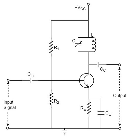
The output can be obtained from the coupling capacitor CC as shown above or from a secondary winding placed at L.
Operation
The high frequency signal that has to be amplified is applied at the input of the amplifier. The resonant frequency of the parallel tuned circuit is made equal to the frequency of the signal applied by altering the capacitance value of the capacitor C, in the tuned circuit.
At this stage, the tuned circuit offers high impedance to the signal frequency, which helps to offer high output across the tuned circuit. As high impedance is offered only for the tuned frequency, all the other frequencies which get lower impedance are rejected by the tuned circuit. Hence the tuned amplifier selects and amplifies the desired frequency signal.
Frequency Response
The parallel resonance occurs at resonant frequency fr when the circuit has a high Q. the resonant frequency fr is given by
$$f_r = \frac{1}{2 \pi \sqrt{LC}}$$
The following graph shows the frequency response of a single tuned amplifier circuit.
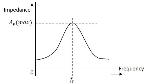
At resonant frequency fr the impedance of parallel tuned circuit is very high and is purely resistive. The voltage across RL is therefore maximum, when the circuit is tuned to resonant frequency. Hence the voltage gain is maximum at resonant frequency and drops off above and below it. The higher the Q, the narrower will the curve be.
Double Tuned Amplifier
An amplifier circuit with a double tuner section being at the collector of the amplifier circuit is called as Double tuner amplifier circuit.
Construction
The construction of double tuned amplifier is understood by having a look at the following figure. This circuit consists of two tuned circuits L1C1 and L2C2 in the collector section of the amplifier. The signal at the output of the tuned circuit L1C1 is coupled to the other tuned circuit L2C2 through mutual coupling method. The remaining circuit details are same as in the single tuned amplifier circuit, as shown in the following circuit diagram.
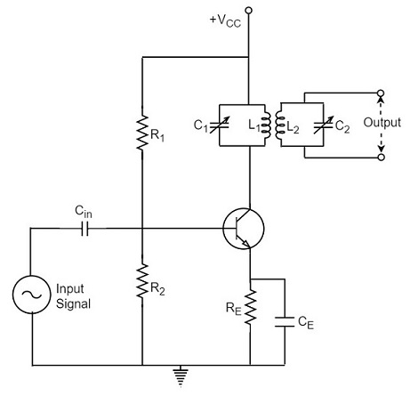
Operation
The high frequency signal which has to be amplified is given to the input of the amplifier. The tuning circuit L1C1 is tuned to the input signal frequency. At this condition, the tuned circuit offers high reactance to the signal frequency. Consequently, large output appears at the output of the tuned circuit L1C1 which is then coupled to the other tuned circuit L2C2 through mutual induction. These double tuned circuits are extensively used for coupling various circuits of radio and television receivers.
Frequency Response of Double Tuned Amplifier
The double tuned amplifier has the special feature of coupling which is important in determining the frequency response of the amplifier. The amount of mutual inductance between the two tuned circuits states the degree of coupling, which determines the frequency response of the circuit.
In order to have an idea on the mutual inductance property, let us go through the basic principle.
Mutual Inductance
As the current carrying coil produces some magnetic field around it, if another coil is brought near this coil, such that it is in the magnetic flux region of the primary, then the varying magnetic flux induces an EMF in the second coil. If this first coil is called as Primary coil, the second one can be called as a Secondary coil.
When the EMF is induced in the secondary coil due to the varying magnetic field of the primary coil, then such phenomenon is called as the Mutual Inductance.
The figure below gives an idea about this.
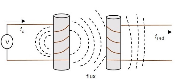
The current is in the figure indicate the source current while iind indicates the induced current. The flux represents the magnetic flux created around the coil. This spreads to the secondary coil also.
With the application of voltage, the current is flows and flux gets created. When the current is varies the flux gets varied, producing iind in the secondary coil, due to the Mutual inductance property.
Coupling
Under the concept of mutual inductance coupling will be as shown in the figure below.
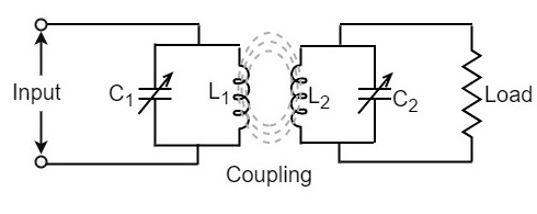
When the coils are spaced apart, the flux linkages of primary coil L1 will not link the secondary coil L2. At this condition, the coils are said to have Loose coupling. The resistance reflected from the secondary coil at this condition is small and the resonance curve will be sharp and the circuit Q is high as shown in the figure below.
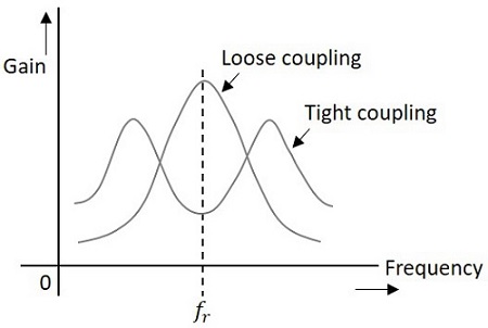
On the contrary, when the primary and secondary coils are brought close together, they have Tight coupling. Under such conditions, the reflected resistance will be large and the circuit Q is lower. Two positions of gain maxima, one above and the other below the resonant frequency are obtained.
Bandwidth of Double Tuned Circuit
The above figure clearly states that the bandwidth increases with the degree of coupling. The determining factor in a double tuned circuit is not Q but the coupling.
We understood that, for a given frequency, the tighter the coupling the greater the bandwidth will be.
The equation for bandwidth is given as
$$BW_{dt} = k f_r$$
Where BWdt = bandwidth for double tuned circuit, K = coefficient of coupling, and fr = resonant frequency.
We hope that now you have gained sufficient knowledge regarding the functioning of tuned amplifiers. In the next chapter, we will learn about feedback amplifiers.
Amplifiers Feedback
An amplifier circuit simply increases the signal strength. But while amplifying, it just increases the strength of its input signal whether it contains information or some noise along with information. This noise or some disturbance is introduced in the amplifiers because of their strong tendency to introduce hum due to sudden temperature changes or stray electric and magnetic fields. Therefore, every high gain amplifier tends to give noise along with signal in its output, which is very undesirable.
The noise level in the amplifier circuits can be considerably reduced by using negative feedback done by injecting a fraction of output in phase opposition to the input signal.
Principle of Feedback Amplifier
A feedback amplifier generally consists of two parts. They are the amplifier and the feedback circuit. The feedback circuit usually consists of resistors. The concept of feedback amplifier can be understood from the following figure.
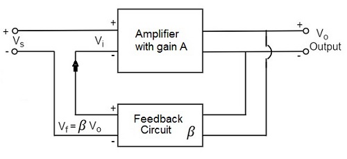
From the above figure, the gain of the amplifier is represented as A. the gain of the amplifier is the ratio of output voltage Vo to the input voltage Vi. the feedback network extracts a voltage Vf = β Vo from the output Vo of the amplifier.
This voltage is added for positive feedback and subtracted for negative feedback, from the signal voltage Vs. Now,
$$V_i = V_s + V_f = V_s + \beta V_o$$
$$V_i = V_s - V_f = V_s - \beta V_o$$
The quantity β = Vf/Vo is called as feedback ratio or feedback fraction.
Let us consider the case of negative feedback. The output Vo must be equal to the input voltage (Vs - βVo) multiplied by the gain A of the amplifier.
Hence,
$$(V_s - \beta V_o)A = V_o$$
Or
$$A V_s - A \beta V_o = V_o$$
Or
$$A V_s = V_o (1 + A \beta)$$
Therefore,
$$\frac{V_o}{V_s} = \frac{A}{1 + A \beta}$$
Let Af be the overall gain (gain with the feedback) of the amplifier. This is defined as the ratio of output voltage Vo to the applied signal voltage Vs, i.e.,
$$A_f = \frac{Output \: voltage}{Input \: signal \: voltage} = \frac{V_o}{V_s}$$
So, from the above two equations, we can understand that,
The equation of gain of the feedback amplifier, with negative feedback is given by
$$A_f = \frac{A}{1 + A \beta}$$
The equation of gain of the feedback amplifier, with positive feedback is given by
$$A_f = \frac{A}{1 - A \beta}$$
These are the standard equations to calculate the gain of feedback amplifiers.
Types of Feedbacks
The process of injecting a fraction of output energy of some device back to the input is known as Feedback. It has been found that feedback is very useful in reducing noise and making the amplifier operation stable.
Depending upon whether the feedback signal aids or opposes the input signal, there are two types of feedbacks used.
Positive Feedback
The feedback in which the feedback energy i.e., either voltage or current is in phase with the input signal and thus aids it is called as Positive feedback.
Both the input signal and feedback signal introduces a phase shift of 180o thus making a 360o resultant phase shift around the loop, to be finally in phase with the input signal.
Though the positive feedback increases the gain of the amplifier, it has the disadvantages such as
- Increasing distortion
- Instability
It is because of these disadvantages the positive feedback is not recommended for the amplifiers. If the positive feedback is sufficiently large, it leads to oscillations, by which oscillator circuits are formed. This concept will be discussed in OSCILLATORS tutorial.
Negative Feedback
The feedback in which the feedback energy i.e., either voltage or current is out of phase with the input and thus opposes it, is called as negative feedback.
In negative feedback, the amplifier introduces a phase shift of 180o into the circuit while the feedback network is so designed that it produces no phase shift or zero phase shift. Thus the resultant feedback voltage Vf is 180o out of phase with the input signal Vin.
Though the gain of negative feedback amplifier is reduced, there are many advantages of negative feedback such as
- Stability of gain is improved
- Reduction in distortion
- Reduction in noise
- Increase in input impedance
- Decrease in output impedance
- Increase in the range of uniform application
It is because of these advantages negative feedback is frequently employed in amplifiers.
Amplifiers Negative Feedback
Negative feedback in an amplifier is the method of feeding a portion of the amplified output to the input but in opposite phase. The phase opposition occurs as the amplifier provides 180o phase shift whereas the feedback network doesn’t.
While the output energy is being applied to the input, for the voltage energy to be taken as feedback, the output is taken in shunt connection and for the current energy to be taken as feedback, the output is taken in series connection.
There are two main types of negative feedback circuits. They are −
- Negative Voltage Feedback
- Negative Current Feedback
Negative Voltage Feedback
In this method, the voltage feedback to the input of amplifier is proportional to the output voltage. This is further classified into two types −
- Voltage-series feedback
- Voltage-shunt feedback
Negative Current Feedback
In this method, the voltage feedback to the input of amplifier is proportional to the output current. This is further classified into two types.
- Current-series feedback
- Current-shunt feedback
Let us have a brief idea on all of them.
Voltage-Series Feedback
In the voltage series feedback circuit, a fraction of the output voltage is applied in series with the input voltage through the feedback circuit. This is also known as shunt-driven series-fed feedback, i.e., a parallel-series circuit.
The following figure shows the block diagram of voltage series feedback, by which it is evident that the feedback circuit is placed in shunt with the output but in series with the input.
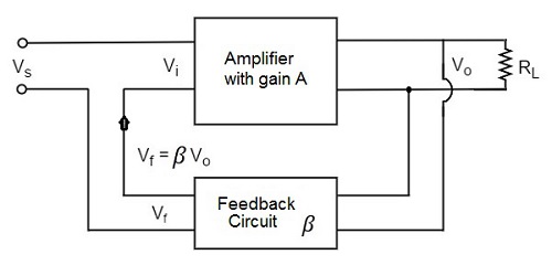
As the feedback circuit is connected in shunt with the output, the output impedance is decreased and due to the series connection with the input, the input impedance is increased.
Voltage-Shunt Feedback
In the voltage shunt feedback circuit, a fraction of the output voltage is applied in parallel with the input voltage through the feedback network. This is also known as shunt-driven shunt-fed feedback i.e., a parallel-parallel proto type.
The below figure shows the block diagram of voltage shunt feedback, by which it is evident that the feedback circuit is placed in shunt with the output and also with the input.
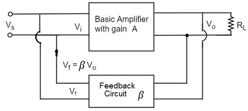
As the feedback circuit is connected in shunt with the output and the input as well, both the output impedance and the input impedance are decreased.
Current-Series Feedback
In the current series feedback circuit, a fraction of the output voltage is applied in series with the input voltage through the feedback circuit. This is also known as series-driven series-fed feedback i.e., a series-series circuit.
The following figure shows the block diagram of current series feedback, by which it is evident that the feedback circuit is placed in series with the output and also with the input.
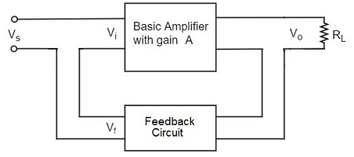
As the feedback circuit is connected in series with the output and the input as well, both the output impedance and the input impedance are increased.
Current-Shunt Feedback
In the current shunt feedback circuit, a fraction of the output voltage is applied in series with the input voltage through the feedback circuit. This is also known as series-driven shunt-fed feedback i.e., a series-parallel circuit.
The below figure shows the block diagram of current shunt feedback, by which it is evident that the feedback circuit is placed in series with the output but in parallel with the input.
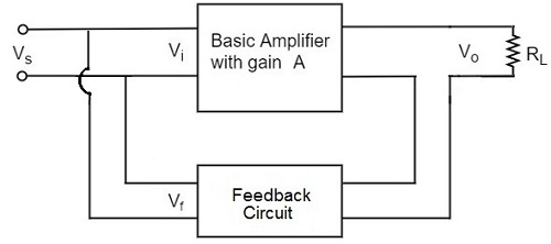
As the feedback circuit is connected in series with the output, the output impedance is increased and due to the parallel connection with the input, the input impedance is decreased.
Let us now tabulate the amplifier characteristics that get affected by different types of negative feedbacks.
| Characteristics | Types of Feedback | |||
|---|---|---|---|---|
| Voltage-Series | Voltage-Shunt | Current-Series | Current-Shunt | |
| Voltage Gain | Decreases | Decreases | Decreases | Decreases |
| Bandwidth | Increases | Increases | Increases | Increases |
| Input resistance | Increases | Decreases | Increases | Decreases |
| Output resistance | Decreases | Decreases | Increases | Increases |
| Harmonic distortion | Decreases | Decreases | Decreases | Decreases |
| Noise | Decreases | Decreases | Decreases | Decreases |
Emitter Follower & Darlington Amplifier
Emitter follower and darlington amplifier are the most common examples for feedback amplifiers. These are the mostly used ones with a number of applications.
Emitter Follower
Emitter follower circuit has a prominent place in feedback amplifiers. Emitter follower is a case of negative current feedback circuit. This is mostly used as a last stage amplifier in signal generator circuits.
The important features of Emitter Follower are −
- It has high input impedance
- It has low output impedance
- It is ideal circuit for impedance matching
All these ideal features allow many applications for the emitter follower circuit. This is a current amplifier circuit that has no voltage gain.
Construction
The constructional details of an emitter follower circuit are nearly similar to a normal amplifier. The main difference is that the load RL is absent at the collector terminal, but present at the emitter terminal of the circuit. Thus the output is taken from the emitter terminal instead of collector terminal.
The biasing is provided either by base resistor method or by potential divider method. The following figure shows the circuit diagram of an Emitter Follower.
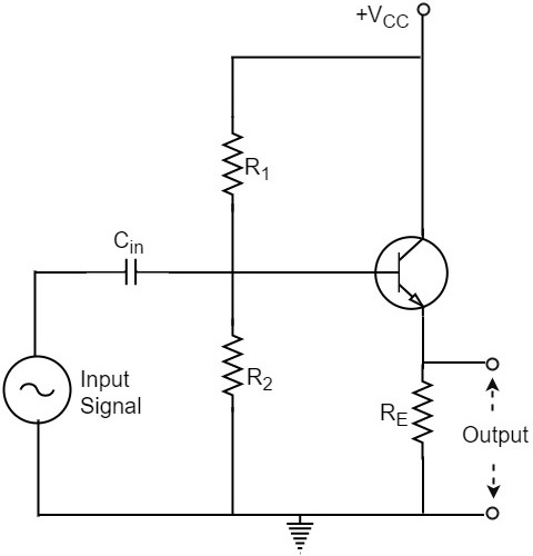
Operation
The input signal voltage applied between base and emitter, develops an output voltage Vo across RE, which is in the emitter section. Therefore,
$$V_o = I_E R_E$$
The whole of this output current is applied to the input through feedback. Hence,
$$V_f = V_o$$
As the output voltage developed across RL is proportional to the emitter current, this emitter follower circuit is a current feedback circuit. Hence,
$$\beta = \frac{V_f}{V_o} = 1$$
It is also noted that the input signal voltage to the transistor (= Vi) is equal to the difference of Vs and Vo i.e.,
$$V_i = V_s - V_o$$
Hence the feedback is negative.
Characteristics
The major characteristics of the emitter follower are as follows −
- No voltage gain. In fact, the voltage gain is nearly 1.
- Relatively high current gain and power gain.
- High input impedance and low output impedance.
- Input and output ac voltages are in phase.
Voltage Gain of Emitter Follower
As the Emitter Follower circuit is a prominent one, let us try to get the equation for the voltage gain of an emitter follower circuit. Our Emitter Follower circuit looks as follows −
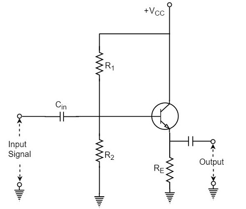
If an AC equivalent circuit of the above circuit is drawn, it would look like the below one, as the emitter by pass capacitor is absent.
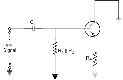
The AC resistance rE of the emitter circuit is given by
$$r_E = r’_E + R_E$$
Where
$$r’_E = \frac{25 mV}{I_E}$$
In order to find the voltage gain of the amplifier, the above figure can be replaced by the following figure.
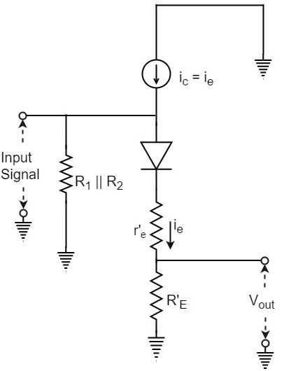
Note that input voltage is applied across the ac resistance of the emitter circuit i.e., (r’E + RE). Assuming the emitter diode to be ideal, the output voltage Vout will be
$$V_{out} = i_e R_E$$
Input voltage Vin will be
$$V_{in} = i_e(r’_e + R_E)$$
Therefore, the Voltage Gain of emitter follower is
$$A_V = \frac{V_{out}}{V_{in}} = \frac{i_e R_E}{i_e(r’_e + R_E)} = \frac{R_E}{(r’_e + R_E)}$$
Or
$$A_V = \frac{R_E}{(r’_e + R_E)}$$
In most practical applications,
$$R_E \gg r’_e$$
So, AV ≈ 1. In practice, the voltage gain of an emitter follower is between 0.8 and 0.999.
Darlington Amplifier
The emitter follower circuit which was just discussed lacks to meet the requirements of the circuit current gain (Ai) and the input impedance (Zi). In order to achieve some increase in the overall values of circuit current gain and input impedance, two transistors are connected as shown in the following circuit diagram, which is known as Darlington configuration.
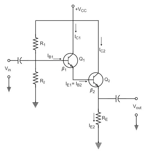
As shown in the above figure, the emitter of the first transistor is connected to the base of the second transistor. The collector terminals of both the transistors are connected together.
Biasing Analysis
Because of this type of connection, the emitter current of the first transistor will also be the base current of the second transistor. Therefore, the current gain of the pair is equal to the product of individual current gains i.e.,
$$\beta = \beta _1 \beta _2$$
A high current gain is generally achieved with a minimum number of components.
As two transistors are used here, two VBE drops are to be considered. The biasing analysis is otherwise similar for one transistor.
Voltage across R2,
$$V_2 = \frac{V_CC}{R_1 + R_2} \times R_2$$
Voltage across RE,
$$V_E = V_2 - 2 V_{BE}$$
Current through RE,
$$I_{E2} = \frac{V_2 - 2 V_{BE}}{R_E}$$
Since the transistors are directly coupled,
$$I_{E1} = I_{B2}$$
Now
$$I_{B2} = \frac{I_{E2}}{\beta _2}$$
Therefore
$$I_{E1} = \frac{I_{E2}}{\beta _2}$$
Which means
$$I_{E1} = I_{E1} \beta _2$$
We have
$I_{E1} = \beta _1 I_{B1}$ since $I_{E1} \cong I_{C1}$
Hence, as
$$I_{E2} = I_{E1} \beta _2$$
We can write
$$I_{E2} = \beta _1 \beta _2 I_{B1}$$
Therefore, Current Gain can be given as
$$\beta = \frac{I_{E2}}{I_{B1}} = \frac{\beta _1 \beta _2 I_{B1}}{I_{B1}} = \beta _1 \beta_2$$
Input impedance of the darling ton amplifier is
$Z_{in} = \beta_1 \beta_2 R_E .....$ neglecting r’e
In practice, these two transistors are placed in a single transistor housing and the three terminals are taken out of the housing as shown in the following figure.
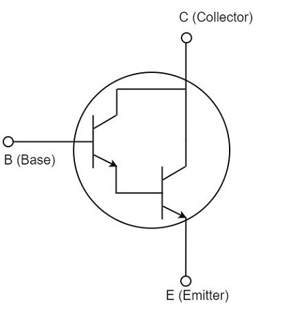
This three terminal device can be called as Darling ton transistor. The darling ton transistor acts like a single transistor that has high current gain and high input impedance.
Characteristics
The following are the important characteristics of Darling ton amplifier.
- Extremely high input impedance (MΩ).
- Extremely high current gain (several thousands).
- Extremely low output impedance (a few Ω).
Since the characteristics of the Darling ton amplifier are basically the same as those of the emitter follower, the two circuits are used for similar applications.
Till now we have discussed amplifiers based on positive feedback. The negative feedback in transistor circuits is helpful in the working of oscillators. The topic of oscillators is entirely covered in Oscillators tutorial.
Noise in Amplifier
An Amplifier, while amplifying just increases the strength of its input signal whether it contains information or some noise along with information. This noise or some disturbance is introduced in the amplifiers because of their strong tendency to introduce hum due to sudden temperature changes or stray electric and magnetic fields.
The performance of an amplifier mainly depends on this Noise. Noise is an unwanted signal that creates disturbance to the desired signal content in the system. This can be an additional signal that is produced within the system or can be some disturbance accompanied with the desired information of the input signal. However, it is unwanted and has to be removed.
A good system is one in which the noise generated by the amplifier itself is small compared to noise from the incoming source.
Noise
Noise is an unwanted signal which interferes with the original message signal and corrupts the parameters of the message signal. This alteration in the communication process, makes the message to get altered after reaching. It is most likely to be entered at the channel or the receiver.
The following graph shows the characteristics of a noise signal.
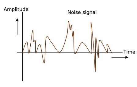
Hence, it is understood that noise is some signal which has no pattern and no constant frequency or amplitude. It is quite random and unpredictable. Measures are usually taken to reduce it, though it can’t be completely eliminated.
Most common examples of noise are −
- “Hiss” sound in radio receivers
- “Buzz” sound amidst of telephone conversations
- “Flicker” in television receivers etc.
Effects of Noise
Noise is an inconvenient feature which affects the system performance. The effects of noise include −
Noise limits the operating range of the systems − Noise indirectly places a limit on the weakest signal that can be amplified by an amplifier. The oscillator in the mixer circuit may limit its frequency because of noise. A system’s operation depends on the operation of its circuits. Noise limits the smallest signal that a receiver is capable of processing.
Noise affects the sensitivity of receivers − Sensitivity is the minimum amount of input signal necessary to obtain the specified quality output. Noise effects the sensitivity of a receiver system, which eventually effects the output.
Signal to Noise Ratio
When a signal is received and it has to be amplified, first the signal is filtered out to remove any unwanted noise if available.
The ratio of the information signal present in the received signal to the noise present is called as Signal to Noise ratio. This ratio has to be higher for a system so that it produces pure information signal unaffected by the unwanted noise.
The SNR can be understood as
$$SNR = \frac{P_{signal}}{P_{noise}}$$
SNR is expressed in logarithmic basis using decibels.
$$SNR_{db} = 10 log_{10}\left (\frac{P_{signal}}{P_{noise}} \right )$$
Signal-to-noise ratio is the ratio of the signal power to the noise power. The higher the value of SNR, the greater will be the quality of the received output.
Types of Noise
The classification of noise is done depending up on the type of source, the effect it shows or the relation it has with the receiver etc.
There are two main ways of which noise gets produced. One is through some external source while the other is created by the internal source, within the receiver section.
External Source
This noise is produced by the external sources which may occur in the medium or channel of communication, usually. This noise can’t be completely eliminated. The best way is to avoid the noise from affecting the signal.
Most common examples of this type of noise are −
- Atmospheric Noise (due to irregularities in atmosphere)
- Extra-terrestrial noise such as solar noise and cosmic noise
- Industrial noise
Internal Source
This noise is produced by the receiver components while functioning. The components in the circuits, due to continuous functioning, may produce few types of noise. This noise is quantifiable. A proper receiver design may lower the effect of this internal noise.
Most common examples of this type of noise are −
Thermal agitation noise (Johnson noise or Electrical noise)
Shot noise (due to random movement of electrons and holes
Transit-time noise (during transition)
Miscellaneous noise is another type of noise which includes flicker, resistance effect and mixer generated noise, etc.
Finally, this gives an overall idea on how a noise will be and how it can affect the amplifier, though present in transmitter or receiver section. The amplifiers that amplify low signals and hence amplify noise in a low level can be called as Low-noise amplifiers.
All the types of amplifiers discussed are more or less subjected to noise in some way or the other. The performance of an amplifier determines its efficiency to deal with the unwanted factors.