
Article Categories
- All Categories
-
 Data Structure
-
 Networking
-
 RDBMS
RDBMS
-
 Operating System
-
 Java
Java
-
 MS Excel
-
 iOS
iOS
-
 HTML
HTML
-
 CSS
CSS
-
 Android
-
 Python
-
 C Programming
-
 C++
C++
-
 C#
C#
-
 MongoDB
-
 MySQL
MySQL
-
 Javascript
-
 PHP
PHP
-
 Economics & Finance
What is Bus Transfer in Computer Architecture?
A bus transfer is the most effective method to send data by using a common bus system. It is constructed using common bus registers in multiple registers. The mechanism of the bus includes a collection of lines. These lines are registers of one bit each, which share only one information at a time. The data transfer is contained by the control signals.
The two methods that can be used in Bus transfer are as follows −
- Using multiplexer
- Using three states bus buffers
Using Multiplexer
A common bus can be generated using a multiplexer. It facilitates in choosing the source register to place the binary data on the bus. The bus register has input and output gating controlled by control signals. The diagram demonstrates the input and output gating of registers.
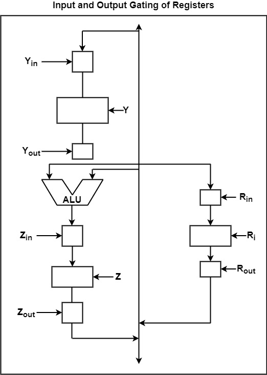
- Ri is the register and Rin and Rout are the input and output gating signals of Ri.
- Z is the register and Zin and Zout are the input and output gating signal of register Z.
- Y is the register and Yin and Yout are the input and output signals of Y.
The figure shows input and output gating. The switches are controlled by control signals. Rin and Rout are the input and output gating of the register Ri. When the signal is ON, Ri is set to 1 and when the signal is OFF, Ri is set to 0.
When the input gating Rin is set to 1, the data is loaded into the register bus Ri accessible on the common bus. When Rout is set to 1, the contents of the register Ri are placed on the data bus. It is referred to as input enabled and output enabled signals. The functions that take place inside the processor are in sync with the clock pulse.
Three-State Buffers
Three-state buffers can generate a common bus. The buffer is an area of the memory, which is added in between the other devices to block several interactions and to connect the support. It is established on the three states, 1, 0, and the open circuit. These three states defines are as follows −
- The logic 0 and 1 are the two signals similar to the ones in the conventional gate.
- The high impedance state defines that it does not contain the logic significance and the output is separated.
- These three-state gates can implement any conventional logic AND or NAND, OR, or NOR.
The diagram demonstrates the logic symbols and the associated truth table.
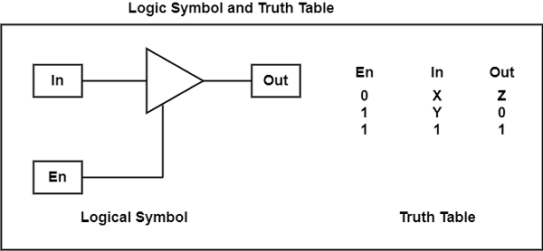
As shown in the figure −
- When the output is allowed and the control input is similar to 1. The logic gate performs as a buffer with the output similar to the input.
- When the input is provided is 0, the gate goes too high impedance state Z and the output is disabled.
- The impedance in three-state buffers linked all the outputs with a cable to produce a common bus line and does not threaten the loading effect.
- The truth table shows that when some input is given and the gate is disabled, it shows in high impedance.
- When the gate is enabled with some input given, then the output results are not in disabled mode.
- When the gate is enabled with input as 1, the output is similar to 1.

23K+ Views
