- Solar Energy - Introduction
- Solar Energy - Photovoltaic Effect
- Developing Solar Panel
- Solar Energy - Cell Efficiency
- Types of Photovoltaics
- Geothermal Energy
- Geothermal Energy - Introduction
- Geothermal Energy - Extraction
- Geothermal Energy - Geophysics
- Hydroelectric Power
- Hydroelectric Power - Introduction
- Hydroelectric Power - Turbine Types
- Hydroelectric Power Systems
- Hydraulic Ram Pump
- Renewable Energy Resources
- Renewable Energy - Quick Guide
- Renewable Energy - Resources
- Renewable Energy - Discussion
Solar Energy - Photovoltaic Effect
It is essential that we have some basic knowledge of PN Junctions before moving on to learn the concept of Photovoltaic Effect.
The PN Junction
The PN Junction was invented by Russell of Bell laboratories in the USA. It refers to a junction between two semiconductors, that is, P-Type and N-type. Russell discovered that the two semiconductors have an interesting behavior at the junction that causes conduction in one direction only.
A P-type semiconductor has holes (absence of electron) as majority charge carriers. An Ntype semiconductor has electrons as majority charge carriers.
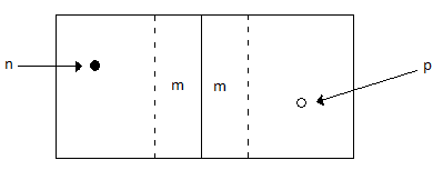
In the diagram given above, at the junction −
Extra charges diffuse across to the opposite junctions such that the positive on the p-side gain negative charges and neutralize them.
Similarly, the negatives at the N-side gain positive charges and neutralize them.
This forms a margin (m) at either side where extra charge are depleted to make this region neutral and at a state of equilibrium. This region is referred to as a depletion layer and no charge from either side crosses.
The depletion layer offers a potential barrier and thus requires external voltage to overcome it. This process is called biasing.
To conduct, in forward biasing, the applied voltage should pump electrons (negative) from n-junction towards the p-side of the junction. Continuous flow of current guarantees a constant movement of electrons to fill holes, hence conduction across the depletion layer.
Reversing the applied voltage, in a process called reverse biasing, causes holes and electrons to drift apart, increasing the depletion layer.
An external load is connected to a solar cell with positive terminal connected to the N- side wafers and the negative terminal to the P- side wafers. A potential difference is created by photovoltaic effect.
The current obtained by electrons displaced by photons is not sufficient to give significant potential difference. The current is therefore contained to cause further collisions and release more electrons.
Photovoltaic Effect
A solar cell utilizes the concept of a p-n junction in capturing the solar energy. The following figure shows the fermi level of a semiconductor.
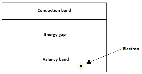
For a semiconductor to conduct, electrons must cross the energy gap from the valence band to the conduction band. These electrons require some energy to dislodge and move across the valence gap. In solar cells, photons emitted from the Sun provide the required energy to overcome the gap.
A photon incident on the surface could be absorbed, reflected, or transmitted. If it is reflected or transmitted, it does not help dislodge an electron and is thus wasted. Therefore, a photon must be absorbed to provide the energy required to dislodge and move electrons across the valence gap.
If Eph is the energy of a photon and EG is the threshold energy to cross the energy gap, then the possible outcomes, when photon hits the surface of a semiconductor are −
Eph < EG − In this case, the photon does not attain the threshold and will just pass through.
Eph = EG − The photon has the exact threshold to dislodge an electron and create a hole electron pair.
Eph > EG − The photon energy surpasses the threshold. This creates an electron-hole pair, though it is a waste, since the electron moves back down the energy gap.
Absorption of solar radiation
In most cases, absorption coefficient of the semiconductor is used to determine the efficiency of absorbing energy from Sun. Low coefficient means poor absorption. Therefore, how far a photon goes is a factor of both absorption coefficient (α) and wavelength of the radiation (λ).
$$\alpha\:=\:\frac{4\pi k}{\lambda}$$
Where, k is the extinction coefficient.
