
Article Categories
- All Categories
-
 Data Structure
-
 Networking
-
 RDBMS
RDBMS
-
 Operating System
-
 Java
Java
-
 MS Excel
-
 iOS
iOS
-
 HTML
HTML
-
 CSS
CSS
-
 Android
-
 Python
-
 C Programming
-
 C++
C++
-
 C#
C#
-
 MongoDB
-
 MySQL
MySQL
-
 Javascript
-
 PHP
PHP
-
 Economics & Finance
27128-20 Compatibility check with 8085AH in 8085 Microprocessor
Let’s perform the memory compatibility check with respect to tAD, tLDR, and tRD parameters.
Compatibility with respect to tAD: The time interval between valid address on the addresses ranging from A15 to A0 and valid data on the addresses ranges from AD7 to AD0. For 8085AH the T state working is 320 nS, but it consists of a maximum of 575 nS. But here the valid data is available for 365 nS. So the speed of the memory is compatible, with an excess time margin of 575 nS - 365 nS = 210 nS.
Compatibility with respect to tLDR: The time interval between the edge of trailing of Arithmetic Logical Unit and valid data on the addresses ranging from AD7- a read operation. For 8085AH working with a T state of 320 nS, it is a maximum of 460 nS. The trailing edge of ALE occurs at 115 nS. Thus tLDR in this case is only 365 nS - 115 nS = 250 nS. Thus, the memory speed is compatible, with actually an excess time margin of 460 nS = 250 nS = 210 nS.
Compatibility with respect to tRD: The interval of time between the leading edge of RD* and the valid data on the addresses is equivalent to AD7-0. For the working with a T state of 320 nS, maximum of 300 nS is required. The RD* signal is activated by 8085 AH at 270 nS and the valid data available by it 365 nS.
Thus, 27128-20 EPROM chip is the speed compatible with 8085AH. So the 8085AH gets interfaced with the memory chips, which have the worst case specifications as shown below:
tAcc = 327 nS + 205 nS = 532 nS
tCE = 323 nS + 205 nS = 528 nS
tOE = 75 nS + 205 nS = 280 nS
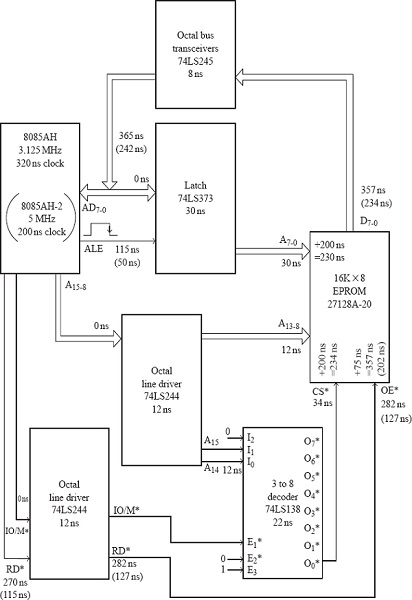
Delays involved in accessing 27128 EPROM in ALS kit.
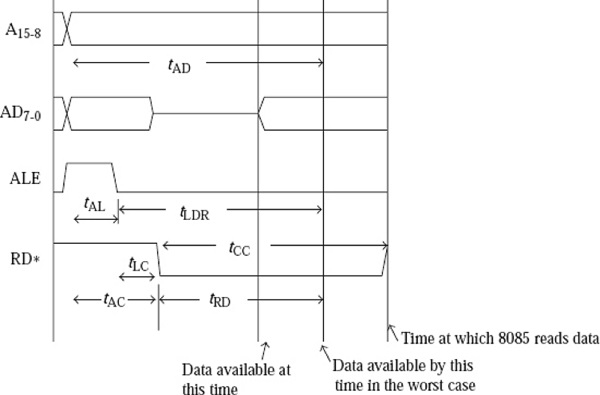
Bus timing characteristics of MR machine cycle

355 Views
