
Article Categories
- All Categories
-
 Data Structure
-
 Networking
-
 RDBMS
RDBMS
-
 Operating System
-
 Java
Java
-
 MS Excel
-
 iOS
iOS
-
 HTML
HTML
-
 CSS
CSS
-
 Android
-
 Python
-
 C Programming
-
 C++
C++
-
 C#
C#
-
 MongoDB
-
 MySQL
MySQL
-
 Javascript
-
 PHP
PHP
-
 Economics & Finance
Interfacing ADC with 8085 Microprocessor
In this section we will see how ADC (Analog to Digital Converter) works with Intel 8085 Microprocessor. The Analog to Digital Conversion is a quantizing process. Here the analog signal is represented by equivalent binary states. The A/D converters can be classified into two groups based on their conversion techniques.
In the first technique it compares given analog signal with the initially generated equivalent signal. In this technique, it includes successive approximation, counter and flash type converters. In another technique it determines the changing of analog signals into time or frequency. This process includes integrator-converters and voltage-to-frequency converters. The first process is faster but less accurate, the second one is more accurate. As the first process uses flash type, so it is expensive and difficult to design for high accuracy.
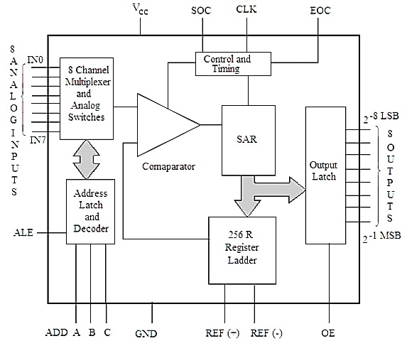
The ADC 0808/0809 Chip
The ADC 0808/0809 is an 8-bit analog to digital converter. It has 8 channel multiplexer to interface with the microprocessor.
This chip is popular and widely used ADC. ADC 0808/0809 is a monolithic CMOS device. This device uses successive approximation technique to convert analog signal to digital form. One of the main advantage of this chip is that it does not require any external zero and full scale adjustment, only +5V DC supply is sufficient.
Let us see some good features of ADC 0808/0809
The conversion speed is much higher
The accuracy is also high
It has minimal temperature dependence
Excellent long term accuracy and repeatability
Less power consumption
The functional block diagram of this chip is like this
Interfacing ADC with 8085 Microprocessor
To interface the ADC with 8085, we need 8255 Programmable Peripheral Interface chip with it. Let us see the circuit diagram of connecting 8085, 8255 and the ADC converter.
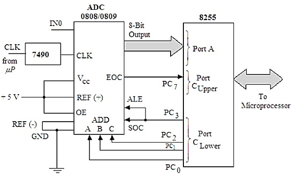
The PortA of 8255 chip is used as the input port. The PC7 pin of Port Cupper is connected to the End of Conversion (EOC) Pin of the analog to digital converter. This port is also used as input port. The Clower port is used as output port. The PC2-0 lines are connected to three address pins of this chip to select input channels. The PC3 pin is connected to the Start of Conversion (SOC) pin and ALE pin of ADC 0808/0809.
Now let us see a program to generate digital signal from analog data. We are using IN0 as input pin, so the pin selection value will be 00H.
Program
   MVI A, 98H ; Set Port A and Cupper as input, CLower as output
   OUT 03H ; Write control word 8255-I to control Word
register
      XRA A ; Clear the accumulator
   OUT 02H ; Send the content of Acc to Port Clower to select
IN0
     MVI A, 08H ; Load the accumulator with 08H
   OUT 02H ; ALE and SOC will be 0
     XRA A ; Clear the accumulator
   OUT 02H ; ALE and SOC will be low.
READ: IN 02H ; Read from EOC (PC7)
   RAL ; Rotate left to check C7 is 1.
JNC READ ; If C7 is not 1, go to READ
IN 00H ; Read digital output of ADC
STA 8000H ; Save result at 8000H
HLT ; Stop the program

35K+ Views
