- Sinusoidal Oscillators Tutorial
- Sinusoidal Oscillators - Home
- Oscillators - Introduction
- Oscillators - Basic Concepts
- Oscillators - Oscillator Circuit
- Tuned Circuit Oscillators
- Oscillators - Hartley Oscillator
- Oscillators - Colpitts Oscillator
- Oscillators - Clapp Oscillator
- Oscillators - Phase Shift Oscillators
- Wien Bridge Oscillator
- Oscillators - Crystal Oscillators
- Negative Resistance Oscillators
- Oscillators - Tunnel Diode Oscillator
- Sinusoidal Oscillators Resources
- Sinusoidal Oscillators - Quick Guide
- Sinusoidal Oscillators - Resources
- Sinusoidal Oscillators - Discussion
Sinusoidal Oscillators - Quick Guide
Sinusoidal Oscillators - Introduction
An oscillator generates output without any ac input signal. An electronic oscillator is a circuit which converts dc energy into ac at a very high frequency. An amplifier with a positive feedback can be understood as an oscillator.
Amplifier vs. Oscillator
An amplifier increases the signal strength of the input signal applied, whereas an oscillator generates a signal without that input signal, but it requires dc for its operation. This is the main difference between an amplifier and an oscillator.
Take a look at the following illustration. It clearly shows how an amplifier takes energy from d.c. power source and converts it into a.c. energy at signal frequency. An oscillator produces an oscillating a.c. signal on its own.
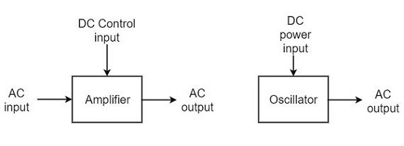
The frequency, waveform, and magnitude of a.c. power generated by an amplifier, is controlled by the a.c. signal voltage applied at the input, whereas those for an oscillator are controlled by the components in the circuit itself, which means no external controlling voltage is required.
Alternator vs. Oscillator
An alternator is a mechanical device that produces sinusoidal waves without any input. This a.c. generating machine is used to generate frequencies up to 1000Hz. The output frequency depends on the number of poles and the speed of rotation of the armature.
The following points highlight the differences between an alternator and an oscillator −
An alternator converts mechanical energy to a.c. energy, whereas the oscillator converts d.c. energy into a.c. energy.
An oscillator can produce higher frequencies of several MHz whereas an alternator cannot.
An alternator has rotating parts, whereas an electronic oscillator doesn’t.
It is easy to change the frequency of oscillations in an oscillator than in an alternator.
Oscillators can also be considered as opposite to rectifiers that convert a.c. to d.c. as these convert d.c. to a.c. You can get a detailed description on rectifiers in our Electronic Circuits tutorial.
Classification of Oscillators
Electronic oscillators are classified mainly into the following two categories −
Sinusoidal Oscillators − The oscillators that produce an output having a sine waveform are called sinusoidal or harmonic oscillators. Such oscillators can provide output at frequencies ranging from 20 Hz to 1 GHz.
Non-sinusoidal Oscillators − The oscillators that produce an output having a square, rectangular or saw-tooth waveform are called non-sinusoidal or relaxation oscillators. Such oscillators can provide output at frequencies ranging from 0 Hz to 20 MHz.
We will discuss only about Sinusoidal Oscillators in this tutorial. You can learn the functions of non-sinusoidal oscillators from our Pulse Circuits tutorial.
Sinusoidal Oscillators
Sinusoidal oscillators can be classified in the following categories −
Tuned Circuit Oscillators − These oscillators use a tuned-circuit consisting of inductors (L) and capacitors (C) and are used to generate high-frequency signals. Thus they are also known as radio frequency R.F. oscillators. Such oscillators are Hartley, Colpitts, Clapp-oscillators etc.
RC Oscillators − There oscillators use resistors and capacitors and are used to generate low or audio-frequency signals. Thus they are also known as audio-frequency (A.F.) oscillators. Such oscillators are Phase –shift and Wein-bridge oscillators.
Crystal Oscillators − These oscillators use quartz crystals and are used to generate highly stabilized output signal with frequencies up to 10 MHz. The Piezo oscillator is an example of a crystal oscillator.
Negative-resistance Oscillator − These oscillators use negative-resistance characteristic of the devices such as tunnel devices. A tuned diode oscillator is an example of a negative-resistance oscillator.
Nature of Sinusoidal Oscillations
The nature of oscillations in a sinusoidal wave are generally of two types. They are damped and undamped oscillations.
Damped Oscillations
The electrical oscillations whose amplitude goes on decreasing with time are called as Damped Oscillations. The frequency of the damped oscillations may remain constant depending upon the circuit parameters.
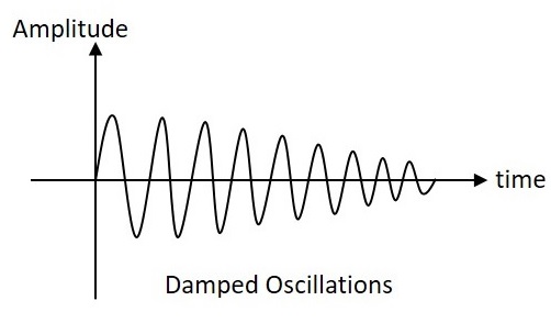
Damped oscillations are generally produced by the oscillatory circuits that produce power losses and doesn’t compensate if required.
Undamped Oscillations
The electrical oscillations whose amplitude remains constant with time are called as Undamped Oscillations. The frequency of the Undamped oscillations remains constant.
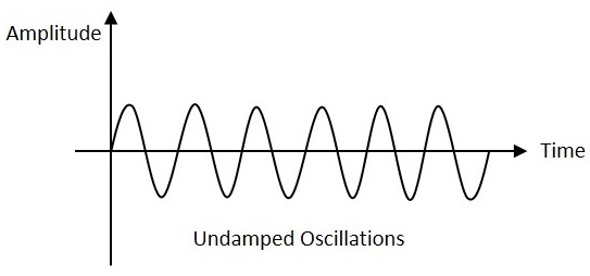
Undamped oscillations are generally produced by the oscillatory circuits that produce no power losses and follow compensation techniques if any power losses occur.
Sinusoidal Oscillators - Basic Concepts
An amplifier with positive feedback produces its output to be in phase with the input and increases the strength of the signal. Positive feedback is also called as degenerative feedback or direct feedback. This kind of feedback makes a feedback amplifier, an oscillator.
The use of positive feedback results in a feedback amplifier having closed-loop gain greater than the open-loop gain. It results in instability and operates as an oscillatory circuit. An oscillatory circuit provides a constantly varying amplified output signal of any desired frequency.
The Oscillatory Circuit
An oscillatory circuit produces electrical oscillations of a desired frequency. They are also known as tank circuits.
A simple tank circuit comprises of an inductor L and a capacitor C both of which together determine the oscillatory frequency of the circuit.
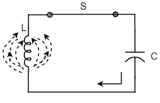
To understand the concept of oscillatory circuit, let us consider the following circuit. The capacitor in this circuit is already charged using a dc source. In this situation, the upper plate of the capacitor has excess of electrons whereas the lower plate has deficit of electrons. The capacitor holds some electrostatic energy and there is a voltage across the capacitor.
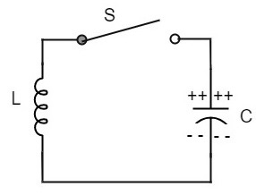
When the switch S is closed, the capacitor discharges and the current flows through the inductor. Due to the inductive effect, the current builds up slowly towards a maximum value. Once the capacitor discharges completely, the magnetic field around the coil is maximum.
Now, let us move on to the next stage. Once the capacitor is discharged completely, the magnetic field begins to collapse and produces a counter EMF according to Lenz’s law. The capacitor is now charged with positive charge on the upper plate and negative charge on the lower plate.
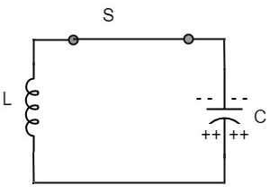
Once the capacitor is fully charged, it starts to discharge to build up a magnetic field around the coil, as shown in the following circuit diagram.
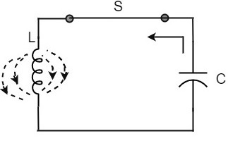
This continuation of charging and discharging results in alternating motion of electrons or an oscillatory current. The interchange of energy between L and C produce continuous oscillations.
In an ideal circuit, where there are no losses, the oscillations would continue indefinitely. In a practical tank circuit, there occur losses such as resistive and radiation losses in the coil and dielectric losses in the capacitor. These losses result in damped oscillations.
Frequency of Oscillations
The frequency of the oscillations produced by the tank circuit are determined by the components of the tank circuit, the L and the C. The actual frequency of oscillations is the resonant frequency (or natural frequency) of the tank circuit which is given by
$$f_r = \frac{1}{2 \pi \sqrt{LC}}$$
Capacitance of the capacitor
The frequency of oscillation fo is inversely proportional to the square root of the capacitance of a capacitor. So, if the value of the capacitor used is large, the charge and discharge time periods will be large. Hence the frequency will be lower.
Mathematically, the frequency,
$$f_o \propto 1\sqrt{C}$$
Self-Inductance of the coil
The frequency of the oscillation fo is proportional to the square root of the self-inductance of the coil. If the value of the inductance is large, the opposition to change of current flow is greater and hence the time required to complete each cycle will be longer, which means time period will be longer and frequency will be lower.
Mathematically, the frequency,
$$f_o \propto 1\sqrt{L}$$
Combining both the above equations,
$$f_o \propto \frac{1}{\sqrt{LC}}$$
$$f_o = \frac{1}{2 \pi \sqrt{LC}}$$
The above equation, though indicates the output frequency, matches the natural frequency or resonance frequency of the tank circuit.
Oscillator Circuit
An Oscillator circuit is a complete set of all the parts of circuit which helps to produce the oscillations. These oscillations should sustain and should be Undamped as just discussed before. Let us try to analyze a practical Oscillator circuit to have a better understanding on how an Oscillator circuit works.
Practical Oscillator Circuit
A Practical Oscillator circuit consists of a tank circuit, a transistor amplifier, and a feedback circuit. The following circuit diagram shows the arrangement of a practical oscillator.
Let us now discuss the parts of this practical oscillator circuit.
Tank Circuit − The tank circuit consists of an inductance L connected in parallel with capacitor C. The values of these two components determine the frequency of the oscillator circuit and hence this is called as Frequency determining circuit.
Transistor Amplifier − The output of the tank circuit is connected to the amplifier circuit so that the oscillations produced by the tank circuit are amplified here. Hence the output of these oscillations are increased by the amplifier.
Feedback Circuit − The function of feedback circuit is to transfer a part of the output energy to LC circuit in proper phase. This feedback is positive in oscillators while negative in amplifiers.
Frequency Stability of an Oscillator
The frequency stability of an oscillator is a measure of its ability to maintain a constant frequency, over a long time interval. When operated over a longer period of time, the oscillator frequency may have a drift from the previously set value either by increasing or by decreasing.
The change in oscillator frequency may arise due to the following factors −
Operating point of the active device such as BJT or FET used should lie in the linear region of the amplifier. Its deviation will affect the oscillator frequency.
The temperature dependency of the performance of circuit components affect the oscillator frequency.
The changes in d.c. supply voltage applied to the active device, shift the oscillator frequency. This can be avoided if a regulated power supply is used.
A change in output load may cause a change in the Q-factor of the tank circuit, thereby causing a change in oscillator output frequency.
The presence of inter element capacitances and stray capacitances affect the oscillator output frequency and thus frequency stability.
The Barkhausen Criterion
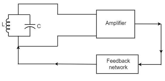
With the knowledge we have till now, we understood that a practical oscillator circuit consists of a tank circuit, a transistor amplifier circuit and a feedback circuit. so, let us now try to brush up the concept of feedback amplifiers, to derive the gain of the feedback amplifiers.
Principle of Feedback Amplifier
A feedback amplifier generally consists of two parts. They are the amplifier and the feedback circuit. The feedback circuit usually consists of resistors. The concept of feedback amplifier can be understood from the following figure below.
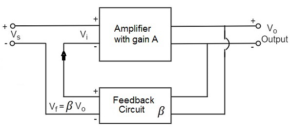
From the above figure, the gain of the amplifier is represented as A. The gain of the amplifier is the ratio of output voltage Vo to the input voltage Vi. The feedback network extracts a voltage Vf = β Vo from the output Vo of the amplifier.
This voltage is added for positive feedback and subtracted for negative feedback, from the signal voltage Vs.
So, for a positive feedback,
Vi = Vs + Vf = Vs + β Vo
The quantity β = Vf/Vo is called as feedback ratio or feedback fraction.
The output Vo must be equal to the input voltage (Vs + βVo) multiplied by the gain A of the amplifier.
Hence,
$$(V_s + \beta V_o)A = V_o$$
Or
$$AV_s + A\beta V_o = V_o$$
Or
$$AV_s = V_o(1 - A\beta)$$
Therefore
$$\frac{V_o}{V_s} = \frac{A}{1 - A\beta}$$
Let Af be the overall gain (gain with the feedback) of the amplifier. This is defined as the ratio of output voltage Vo to the applied signal voltage Vs, i.e.,
$$A_f = \frac{Output \: Voltage}{Input \: Signal \: Voltage} = \frac{V_o}{V_s}$$
Rrom the above two equations, we can understand that, the equation of gain of the feedback amplifier with positive feedback is given by
$$A_f = \frac{A}{1 - A\beta}$$
Where Aβ is the feedback factor or the loop gain.
If Aβ = 1, Af = ∞. Thus the gain becomes infinity, i.e., there is output without any input. In another words, the amplifier works as an Oscillator.
The condition Aβ = 1 is called as Barkhausen Criterion of oscillations. This is a very important factor to be always kept in mind, in the concept of Oscillators.
Tuned Circuit Oscillators
Tuned circuit oscillators are the circuits that produce oscillations with the help of tuning circuits. The tuning circuits consists of an inductance L and a capacitor C. These are also known as LC oscillators, resonant circuit oscillators or tank circuit oscillators.
The tuned circuit oscillators are used to produce an output with frequencies ranging from 1 MHz to 500 MHz Hence these are also known as R.F. Oscillators. A BJT or a FET is used as an amplifier with tuned circuit oscillators. With an amplifier and an LC tank circuit, we can feedback a signal with right amplitude and phase to maintain oscillations.
Types of Tuned Circuit Oscillators
Most of the oscillators used in radio transmitters and receivers are of LC oscillators type. Depending upon the way the feedback is used in the circuit, the LC oscillators are divided as the following types.
Tuned-collector or Armstrong Oscillator − It uses inductive feedback from the collector of a transistor to the base. The LC circuit is in the collector circuit of the transistor.
Tuned base Oscillator − It uses inductive feedback. But the LC circuit is in the base circuit.
Hartley Oscillator − It uses inductive feedback.
Colpitts Oscillator − It uses capacitive feedback.
Clapp Oscillator − It uses capacitive feedback.
We shall now discuss all the above mentioned LC oscillators in detail.
Tuned Collector Oscillator
Tuned collector oscillators are called so, because the tuned circuit is placed in the collector of the transistor amplifier. The combination of L and C form the tuned circuit or frequency determining circuit.
Construction
The resistors R1, R2 and RE are used to provide d.c. bias to the transistor. The capacitors CE and C are the by-pass capacitors. The secondary of the transformer provides a.c. feedback voltage that appears across the base-emitter junction of R1 and R2 is at a.c. ground due to by-pass capacitor C. In case, the capacitor was absent, a part of the voltage induced in the secondary of the transformer would drop across R2 instead of completely going to the input of transistor.
As the CE configured transistor provides 180o phase shift, another 180o phase shift is provided by the transformer, which makes 360o phase shift between the input and output voltages. The following circuit diagram shows the arrangement of a tuned collector circuit.
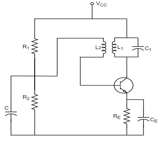
Operation
Once the supply is given, the collector current starts increasing and charging of capacitor C takes place. When the capacitor is fully charged, it discharges through the inductance L1. Now oscillations are produced. These oscillations induce some voltage in the secondary winding L2. The frequency of voltage induced in the secondary winding is same as that of the tank circuit and its magnitude depends upon the number of turns in secondary winding and coupling between both the windings.
The voltage across L2 is applied between base and emitter and appears in the amplified form in the collector circuit, thus overcoming the losses in the tank circuit. The number of turns of L2 and coupling between L1 and L2 are so adjusted that oscillations across L2 are amplified to a level just sufficient to supply losses to the tank circuit.
Tuned collector oscillators are widely used as the local oscillator in radio receivers.
Tuned Base Oscillator
Tuned base oscillators are called so, because the tuned circuit is placed in the base of the transistor amplifier. The combination of L and C form the tuned circuit or frequency determining circuit.
Construction
The resistors R1, R2 and RE are used to provide d.c. bias to the transistor. The parallel combination of Re and Ce in the emitter circuit is the stabilizing circuit. CC is the blocking capacitor. The capacitors CE and C are the by-pass capacitors. The primary coil L and the secondary coil L1 of RF transformer provides the required feedback to collector and base circuits.
As the CE configured transistor provides 180o phase shift, another 180o phase shift is provided by the transformer, which makes 360o phase shift between the input and output voltages. The following circuit diagram shows the arrangement of a tuned base oscillator circuit.
Operation
When the circuit is switched on, the collector current starts rising. As the collector is connected to the coil L1, that current creates some magnetic field around it. This induces a voltage in the tuned circuit coil L. The feedback voltage produces an increase in emitterbase voltage and base current. A further increase in collector current is thus achieved and the cycle continues until the collector current becomes saturated. In the meanwhile, the capacitor is fully charged.
When the collector current reaches saturation level, there is no feedback voltage in L. As the capacitor has been charged fully, it starts discharging through L. This decreases the emitter base bias and hence IB and the collector current also decreases. By the time the collector current reaches cutoff, the capacitor C is fully charged with opposite polarity. As the transistor now gets off, the condenser C begins to discharge through L. This increases the emitter-base bias. As a result, the collector current increases.
The cycle repeats so long as enough energy is supplied to meet the losses in L.C. circuit. The frequency of oscillation is equal to the resonant frequency of L.C. circuit.
Drawback
The main drawback of tuned-base oscillator circuit is that, due to the low base-emitter resistance, which appears in shunt with the tuned circuit, the tank circuit gets loaded. This reduces its Q which in turn causes drift in oscillator frequency. Thus stability becomes poorer. Due to this reason, the tuned circuit is not usually connected in base circuit.
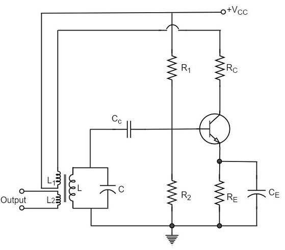
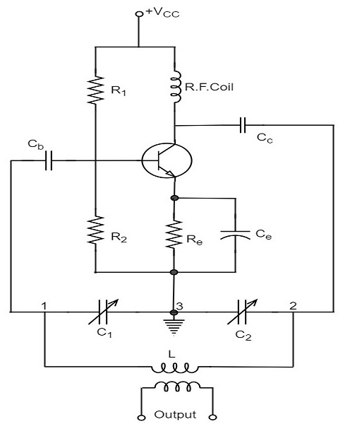
Hartley Oscillator
A very popular local oscillator circuit that is mostly used in radio receivers is the Hartley Oscillator circuit. The constructional details and operation of a Hartley oscillator are as discussed below.
Construction
In the circuit diagram of a Hartley oscillator shown below, the resistors R1, R2 and Re provide necessary bias condition for the circuit. The capacitor Ce provides a.c. ground thereby providing any signal degeneration. This also provides temperature stabilization.
The capacitors Cc and Cb are employed to block d.c. and to provide an a.c. path. The radio frequency choke (R.F.C) offers very high impedance to high frequency currents which means it shorts for d.c. and opens for a.c. Hence it provides d.c. load for collector and keeps a.c. currents out of d.c. supply source
Tank Circuit
The frequency determining network is a parallel resonant circuit which consists of the inductors L1 and L2 along with a variable capacitor C. The junction of L1 and L2 are earthed. The coil L1 has its one end connected to base via Cc and the other to emitter via Ce. So, L2 is in the output circuit. Both the coils L1 and L2 are inductively coupled and together form an Auto-transformer.
The following circuit diagram shows the arrangement of a Hartley oscillator. The tank circuit is shunt fed in this circuit. It can also be a series-fed.
Operation
When the collector supply is given, a transient current is produced in the oscillatory or tank circuit. The oscillatory current in the tank circuit produces a.c. voltage across L1.
The auto-transformer made by the inductive coupling of L1 and L2 helps in determining the frequency and establishes the feedback. As the CE configured transistor provides 180o phase shift, another 180o phase shift is provided by the transformer, which makes 360o phase shift between the input and output voltages.
This makes the feedback positive which is essential for the condition of oscillations. When the loop gain |βA| of the amplifier is greater than one, oscillations are sustained in the circuit.
Frequency
The equation for frequency of Hartley oscillator is given as
$$f = \frac{1}{2 \pi \sqrt{L_T C}}$$
$$L_T = L_1 + L_2 + 2M$$
Here, LT is the total cumulatively coupled inductance; L1 and L2 represent inductances of 1st and 2nd coils; and M represents mutual inductance.
Mutual inductance is calculated when two windings are considered.
Advantages
The advantages of Hartley oscillator are
Instead of using a large transformer, a single coil can be used as an auto-transformer.
Frequency can be varied by employing either a variable capacitor or a variable inductor.
Less number of components are sufficient.
The amplitude of the output remains constant over a fixed frequency range.
Disadvantages
The disadvantages of Hartley oscillator are
- It cannot be a low frequency oscillator.
- Harmonic distortions are present.
Applications
The applications of Hartley oscillator are
- It is used to produce a sinewave of desired frequency.
- Mostly used as a local oscillator in radio receivers.
- It is also used as R.F. Oscillator.
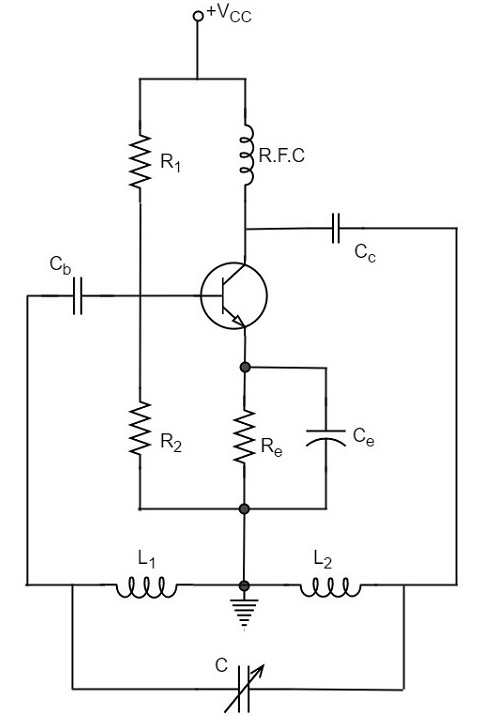
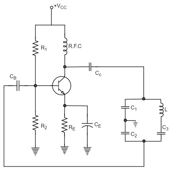
Colpitts Oscillator
A Colpitts oscillator looks just like the Hartley oscillator but the inductors and capacitors are replaced with each other in the tank circuit. The constructional details and operation of a colpitts oscillator are as discussed below.
Construction
Let us first take a look at the circuit diagram of a Colpitts oscillator.
The resistors R1, R2 and Re provide necessary bias condition for the circuit. The capacitor Ce provides a.c. ground thereby providing any signal degeneration. This also provides temperature stabilization.
The capacitors Cc and Cb are employed to block d.c. and to provide an a.c. path. The radio frequency choke (R.F.C) offers very high impedance to high frequency currents which means it shorts for d.c. and opens for a.c. Hence it provides d.c. load for collector and keeps a.c. currents out of d.c. supply source.
Tank Circuit
The frequency determining network is a parallel resonant circuit which consists of variable capacitors C1 and C2 along with an inductor L. The junction of C1 and C2 are earthed. The capacitor C1 has its one end connected to base via Cc and the other to emitter via Ce. the voltage developed across C1 provides the regenerative feedback required for the sustained oscillations.
Operation
When the collector supply is given, a transient current is produced in the oscillatory or tank circuit. The oscillatory current in the tank circuit produces a.c. voltage across C1 which are applied to the base emitter junction and appear in the amplified form in the collector circuit and supply losses to the tank circuit.
If terminal 1 is at positive potential with respect to terminal 3 at any instant, then terminal 2 will be at negative potential with respect to 3 at that instant because terminal 3 is grounded. Therefore, points 1 and 2 are out of phase by 180o.
As the CE configured transistor provides 180o phase shift, it makes 360o phase shift between the input and output voltages. Hence, feedback is properly phased to produce continuous Undamped oscillations. When the loop gain |βA| of the amplifier is greater than one, oscillations are sustained in the circuit.
Frequency
The equation for frequency of Colpitts oscillator is given as
$$f = \frac{1}{2 \pi \sqrt{LC_T}}$$
CT is the total capacitance of C1 and C2 connected in series.
$$\frac{1}{C_T} = \frac{1}{C_1} + \frac{1}{C_2}$$
$$C_T = \frac{C_1 \times C_2}{C_1 + C_2}$$
Advantages
The advantages of Colpitts oscillator are as follows −
- Colpitts oscillator can generate sinusoidal signals of very high frequencies.
- It can withstand high and low temperatures.
- The frequency stability is high.
- Frequency can be varied by using both the variable capacitors.
- Less number of components are sufficient.
- The amplitude of the output remains constant over a fixed frequency range.
The Colpitts oscillator is designed to eliminate the disadvantages of Hartley oscillator and is known to have no specific disadvantages. Hence there are many applications of a colpitts oscillator.
Applications
The applications of Colpitts oscillator are as follows −
- Colpitts oscillator can be used as High frequency sinewave generator.
- This can be used as a temperature sensor with some associated circuitry.
- Mostly used as a local oscillator in radio receivers.
- It is also used as R.F. Oscillator.
- It is also used in Mobile applications.
- It has got many other commercial applications.
Clapp Oscillator
Another oscillator which is an advanced version of Colpitts oscillator is the Clapp Oscillator. This circuit is designed by making a few changes to the Colpitts oscillator.
The circuit differs from the Colpitts oscillator only in one respect; it contains one additional capacitor (C3) connected in series with the inductor. The addition of capacitor (C3) improves the frequency stability and eliminates the effect of transistor parameters and stray capacitances.
The following circuit diagram shows the arrangement of a transistor Clapp oscillator.
The operation of Clapp oscillator circuit is in the same way as that of Colpitts oscillator. The frequency of oscillator is given by the relation,
$$f_o = \frac{1}{2 \pi \sqrt{L.C}}$$
Where
$$C = \frac{1}{\frac{1}{C_1} + \frac{1}{C_2} + \frac{1}{C_3}}$$
Usually, the value of C3 is much smaller than C1 and C2. As a result of this, C is approximately equal to C3. Therefore, the frequency of oscillation,
$$f_o = \frac{1}{2 \pi \sqrt{L.C_3}}$$
It is understood that the Clapp oscillator is similar to the Colpitts oscillator, however they differ in the way the inductances and capacitances are arranged. The frequency stability though is good, can be variable in a Clapp oscillator.
A Clapp oscillator is sometimes preferred over a Colpitts oscillator for constructing a variable frequency oscillator. The Clapp oscillators are used in receiver tuning circuits as a frequency oscillator.
Phase Shift Oscillators
One of the important features of an oscillator is that the feedback energy applied should be in correct phase to the tank circuit. The oscillator circuits discussed so far has employed inductor (L) and capacitor (C) combination, in the tank circuit or frequency determining circuit.
We have observed that the LC combination in oscillators provide 180o phase shift and transistor in CE configuration provide 180° phase shift to make a total of 360o phase shift so that it would make a zero difference in phase.
Drawbacks of LC circuits
Though they have few applications, the LC circuits have few drawbacks such as
- Frequency instability
- Waveform is poor
- Cannot be used for low frequencies
- Inductors are bulky and expensive
We have another type of oscillator circuits, which are made by replacing the inductors with resistors. By doing so, the frequency stability is improved and a good quality waveform is obtained. These oscillators can also produce lower frequencies. As well, the circuit becomes neither bulky nor expensive.
All the drawbacks of LC oscillator circuits are thus eliminated in RC oscillator circuits. Hence the need for RC oscillator circuits arise. These are also called as Phase–shift Oscillators.
Principle of Phase-shift oscillators
We know that the output voltage of an RC circuit for a sinewave input leads the input voltage. The phase angle by which it leads is determined by the value of RC components used in the circuit. The following circuit diagram shows a single section of an RC network.
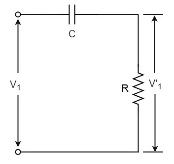
The output voltage V1’ across the resistor R leads the input voltage applied input V1 by some phase angle ɸo. If R were reduced to zero, V1’ will lead the V1 by 90o i.e., ɸo = 90o.
However, adjusting R to zero would be impracticable, because it would lead to no voltage across R. Therefore, in practice, R is varied to such a value that makes V1’ to lead V1 by 60o. The following circuit diagram shows the three sections of the RC network.
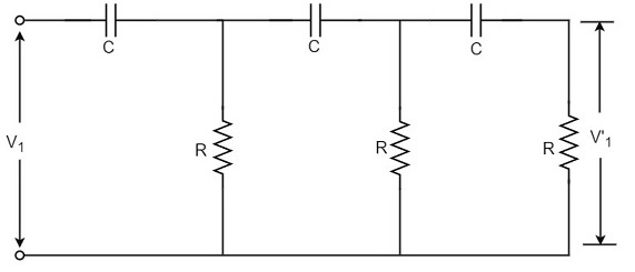
Each section produces a phase shift of 60o. Consequently, a total phase shift of 180o is produced, i.e., voltage V2 leads the voltage V1 by 180o.
Phase-shift Oscillator Circuit
The oscillator circuit that produces a sine wave using a phase-shift network is called as a Phase-shift oscillator circuit. The constructional details and operation of a phase-shift oscillator circuit are as given below.
Construction
The phase-shift oscillator circuit consists of a single transistor amplifier section and a RC phase-shift network. The phase shift network in this circuit, consists of three RC sections. At the resonant frequency fo, the phase shift in each RC section is 60o so that the total phase shift produced by RC network is 180o.
The following circuit diagram shows the arrangement of an RC phase-shift oscillator.
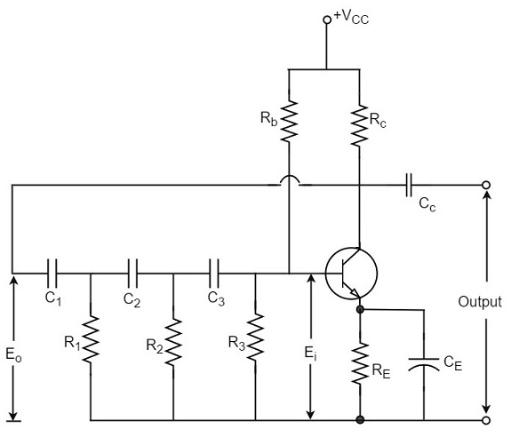
The frequency of oscillations is given by
$$f_o = \frac{1}{2\pi RC \sqrt{6}}$$
Where
$$R_1 = R_2 = R_3 = R$$
$$C_1 = C_2 = C_3 = C$$
Operation
The circuit when switched ON oscillates at the resonant frequency fo. The output Eo of the amplifier is fed back to RC feedback network. This network produces a phase shift of 180o and a voltage Ei appears at its output. This voltage is applied to the transistor amplifier.
The feedback applied will be
$$m = E_i/E_o$$
The feedback is in correct phase, whereas the transistor amplifier, which is in CE configuration, produces a 180o phase shift. The phase shift produced by network and the transistor add to form a phase shift around the entire loop which is 360o.
Advantages
The advantages of RC phase shift oscillator are as follows −
- It does not require transformers or inductors.
- It can be used to produce very low frequencies.
- The circuit provides good frequency stability.
Disadvantages
The disadvantages of RC phase shift oscillator are as follows −
- Starting the oscillations is difficult as the feedback is small.
- The output produced is small.
Wien Bridge Oscillator
Another type of popular audio frequency oscillator is the Wien bridge oscillator circuit. This is mostly used because of its important features. This circuit is free from the circuit fluctuations and the ambient temperature.
The main advantage of this oscillator is that the frequency can be varied in the range of 10Hz to about 1MHz whereas in RC oscillators, the frequency is not varied.
Construction
The circuit construction of Wien bridge oscillator can be explained as below. It is a two-stage amplifier with RC bridge circuit. The bridge circuit has the arms R1C1, R3, R2C2 and the tungsten lamp Lp. Resistance R3 and the lamp Lp are used to stabilize the amplitude of the output.
The following circuit diagram shows the arrangement of a Wien bridge oscillator.
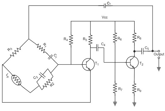
The transistor T1 serves as an oscillator and an amplifier while the other transistor T2 serves as an inverter. The inverter operation provides a phase shift of 180o. This circuit provides positive feedback through R1C1, C2R2 to the transistor T1 and negative feedback through the voltage divider to the input of transistor T2.
The frequency of oscillations is determined by the series element R1C1 and parallel element R2C2 of the bridge.
$$f = \frac{1}{2 \pi \sqrt{R_1C_1R_2C_2}}$$
If R1 = R2 and C1 = C2 = C
Then,
$$f = \frac{1}{2\pi RC}$$
Now, we can simplify the above circuit as follows −
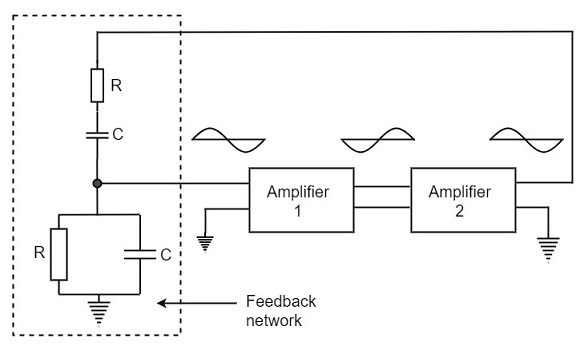
The oscillator consists of two stages of RC coupled amplifier and a feedback network. The voltage across the parallel combination of R and C is fed to the input of amplifier 1. The net phase shift through the two amplifiers is zero.
The usual idea of connecting the output of amplifier 2 to amplifier 1 to provide signal regeneration for oscillator is not applicable here as the amplifier 1 will amplify signals over a wide range of frequencies and hence direct coupling would result in poor frequency stability. By adding Wien bridge feedback network, the oscillator becomes sensitive to a particular frequency and hence frequency stability is achieved.
Operation
When the circuit is switched ON, the bridge circuit produces oscillations of the frequency stated above. The two transistors produce a total phase shift of 360o so that proper positive feedback is ensured. The negative feedback in the circuit ensures constant output. This is achieved by temperature sensitive tungsten lamp Lp. Its resistance increases with current.
If the amplitude of the output increases, more current is produced and more negative feedback is achieved. Due to this, the output would return to the original value. Whereas, if the output tends to decrease, reverse action would take place.
Advantages
The advantages of Wien bridge oscillator are as follows −
The circuit provides good frequency stability.
It provides constant output.
The operation of circuit is quite easy.
The overall gain is high because of two transistors.
The frequency of oscillations can be changed easily.
The amplitude stability of the output voltage can be maintained more accurately, by replacing R2 with a thermistor.
Disadvantages
The disadvantages of Wien bridge oscillator are as follows −
The circuit cannot generate very high frequencies.
Two transistors and number of components are required for the circuit construction.
Crystal Oscillators
Whenever an oscillator is under continuous operation, its frequency stability gets affected. There occur changes in its frequency. The main factors that affect the frequency of an oscillator are
- Power supply variations
- Changes in temperature
- Changes in load or output resistance
In RC and LC oscillators the values of resistance, capacitance and inductance vary with temperature and hence the frequency gets affected. In order to avoid this problem, the piezo electric crystals are being used in oscillators.
The use of piezo electric crystals in parallel resonant circuits provide high frequency stability in oscillators. Such oscillators are called as Crystal Oscillators.
Crystal Oscillators
The principle of crystal oscillators depends upon the Piezo electric effect. The natural shape of a crystal is hexagonal. When a crystal wafer is cur perpendicular to X-axis, it is called as X-cut and when it is cut along Y-axis, it is called as Y-cut.
The crystal used in crystal oscillator exhibits a property called as Piezo electric property. So, let us have an idea on piezo electric effect.
Piezo Electric Effect
The crystal exhibits the property that when a mechanical stress is applied across one of the faces of the crystal, a potential difference is developed across the opposite faces of the crystal. Conversely, when a potential difference is applied across one of the faces, a mechanical stress is produced along the other faces. This is known as Piezo electric effect.
Certain crystalline materials like Rochelle salt, quartz and tourmaline exhibit piezo electric effect and such materials are called as Piezo electric crystals. Quartz is the most commonly used piezo electric crystal because it is inexpensive and readily available in nature.
When a piezo electric crystal is subjected to a proper alternating potential, it vibrates mechanically. The amplitude of mechanical vibrations becomes maximum when the frequency of alternating voltage is equal to the natural frequency of the crystal.
Working of a Quartz Crystal
In order to make a crystal work in an electronic circuit, the crystal is placed between two metal plates in the form of a capacitor. Quartz is the mostly used type of crystal because of its availability and strong nature while being inexpensive. The ac voltage is applied in parallel to the crystal.
The circuit arrangement of a Quartz Crystal will be as shown below −
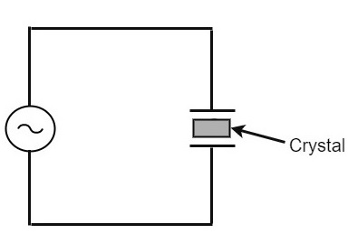
If an AC voltage is applied, the crystal starts vibrating at the frequency of the applied voltage. However, if the frequency of the applied voltage is made equal to the natural frequency of the crystal, resonance takes place and crystal vibrations reach a maximum value. This natural frequency is almost constant.
Equivalent circuit of a Crystal
If we try to represent the crystal with an equivalent electric circuit, we have to consider two cases, i.e., when it vibrates and when it doesn’t. The figures below represent the symbol and electrical equivalent circuit of a crystal respectively.
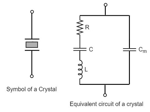
The above equivalent circuit consists of a series R-L-C circuit in parallel with a capacitance Cm. When the crystal mounted across the AC source is not vibrating, it is equivalent to the capacitance Cm. When the crystal vibrates, it acts like a tuned R-L-C circuit.
Frequency response
The frequency response of a crystal is as shown below. The graph shows the reactance (XL or XC) versus frequency (f). It is evident that the crystal has two closely spaced resonant frequencies.
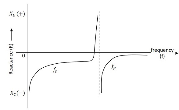
The first one is the series resonant frequency (fs), which occurs when reactance of the inductance (L) is equal to the reactance of the capacitance C. In that case, the impedance of the equivalent circuit is equal to the resistance R and the frequency of oscillation is given by the relation,
$$f = \frac{1}{2\pi \sqrt{L.C}}$$
The second one is the parallel resonant frequency (fp), which occurs when the reactance of R-L-C branch is equal to the reactance of capacitor Cm. At this frequency, the crystal offers a very high impedance to the external circuit and the frequency of oscillation is given by the relation.
$$f_p = \frac{1}{2\pi \sqrt{L.C_T}}$$
Where
$$C_T = \frac{C C_m}{(C + C_m)}$$
The value of Cm is usually very large as compared to C. Therefore, the value of CT is approximately equal to C and hence the series resonant frequency is approximately equal to the parallel resonant frequency (i.e., fs = fp).
Crystal Oscillator Circuit
A crystal oscillator circuit can be constructed in a number of ways like a Crystal controlled tuned collector oscillator, a Colpitts crystal oscillator, a Clap crystal oscillator etc. But the transistor pierce crystal oscillator is the most commonly used one. This is the circuit which is normally referred as a crystal oscillator circuit.
The following circuit diagram shows the arrangement of a transistor pierce crystal oscillator.
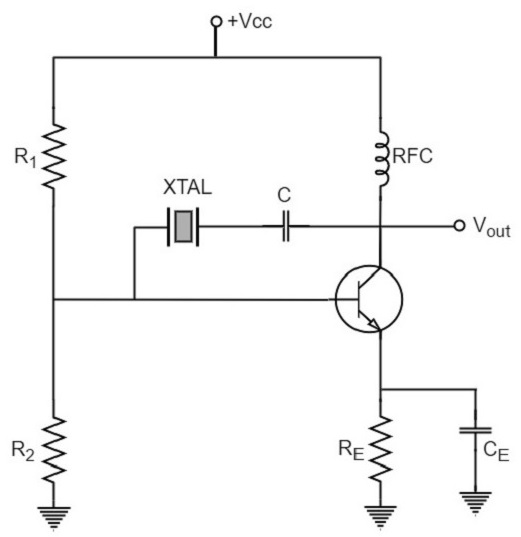
In this circuit, the crystal is connected as a series element in the feedback path from collector to the base. The resistors R1, R2 and RE provide a voltage-divider stabilized d.c. bias circuit. The capacitor CE provides a.c. bypass of the emitter resistor and RFC (radio frequency choke) coil provides for d.c. bias while decoupling any a.c. signal on the power lines from affecting the output signal. The coupling capacitor C has negligible impedance at the circuit operating frequency. But it blocks any d.c. between collector and base.
The circuit frequency of oscillation is set by the series resonant frequency of the crystal and its value is given by the relation,
$$f_o = \frac{1}{2\pi \sqrt{L.C}}$$
It may be noted that the changes in supply voltage, transistor device parameters etc. have no effect on the circuit operating frequency, which is held stabilized by the crystal.
Advantages
The advantages of crystal oscillator are as follows −
- They have a high order of frequency stability.
- The quality factor (Q) of the crystal is very high.
Disadvantages
The disadvantages of crystal oscillator are as follows −
- They are fragile and can be used in low power circuits.
- The frequency of oscillations cannot be changed appreciably.
Frequency Stability of an Oscillator
An Oscillator is expected to maintain its frequency for a longer duration without any variations, so as to have a smoother clear sinewave output for the circuit operation. Hence the term frequency stability really matters a lot, when it comes to oscillators, whether sinusoidal or non-sinusoidal.
The frequency stability of an oscillator is defined as the ability of the oscillator to maintain the required frequency constant over a long time interval as possible. Let us try to discuss the factors that affect this frequency stability.
Change in operating point
We have already come across the transistor parameters and learnt how important an operating point is. The stability of this operating point for the transistor being used in the circuit for amplification (BJT or FET), is of higher consideration.
The operating of the active device used is adjusted to be in the linear portion of its characteristics. This point is shifted due to temperature variations and hence the stability is affected.
Variation in temperature
The tank circuit in the oscillator circuit, contains various frequency determining components such as resistors, capacitors and inductors. All of their parameters are temperature dependent. Due to the change in temperature, their values get affected. This brings the change in frequency of the oscillator circuit.
Due to power supply
The variations in the supplied power will also affect the frequency. The power supply variations lead to the variations in Vcc. This will affect the frequency of the oscillations produced.
In order to avoid this, the regulated power supply system is implemented. This is in short called as RPS. The details of regulated power supply were clearly discussed in the power supply section of ELECTRONIC CIRCUITS tutorial.
Change in output load
The variations in output resistance or output load also affects the frequency of the oscillator. When a load is connected, the effective resistance of the tank circuit is changed. As a result, the Q-factor of LC tuned circuit is changed. This results a change in output frequency of oscillator.
Changes in inter-element capacitances
Inter-element capacitances are the capacitances that develop in PN junction materials such as diodes and transistors. These are developed due to the charge present in them during their operation.
The inter element capacitors undergo change due to various reasons as temperature, voltage etc. This problem can be solved by connecting swamping capacitor across offending inter-element capacitor.
Value of Q
The value of Q (Quality factor) must be high in oscillators. The value of Q in tuned oscillators determine the selectivity. As this Q is directly proportional to the frequency stability of a tuned circuit, the value of Q should be maintained high.
Frequency stability can be mathematically represented as,
$$S_w = d\theta/dw$$
Where dθ is the phase shift introduced for a small frequency change in nominal frequency fr. The circuit giving the larger value of (dθ/dw) has more stable oscillatory frequency.
Negative Resistance Oscillators
An oscillator that works on negative resistance property can termed as a Negative resistance oscillator. The term negative resistance refers to a condition where an increase in voltage across two points causes a decrease in current. Some of the non-linear devices exhibit negative resistance property, under certain conditions.
Negative Resistance Property
Let us observe the behavior when the voltage is applied to a non-linear device that exhibits negative resistance property. To understand this property, let us observe the below graph to find out the variations in voltage and current.
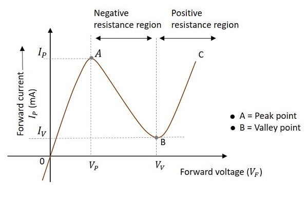
As forward voltage increases, the current increases rapidly and it increases until a peak point, called as Peak Current, denoted by IP. The voltage at this point is called as Peak Voltage, denoted by VP. This point is indicated by A in the above graph. The point A is called Peak Point.
If the voltage is further increased beyond VP, then the current starts decreasing. It decreases until a point, called as Valley Current, denoted by IV. The voltage at this point is called as Valley Voltage, denoted by VV. This point is indicated by B in the above graph. The point B is called Valley Point.
Hence the region between point A and point B indicates the Negative resistance region. Once the valley point is reached and if the voltage is further increased, then the current starts increasing. This means the negative resistance region was ended and the device behaves normally as per Ohm’s law. This region is called as Positive Resistance region, which is indicated by point B to point C in the graph.
Few oscillators exhibit negative resistance property during their operation. The uni-junction oscillator is the best example of a non-sinusoidal oscillator (produces sweep waveform as output) that exhibit negative resistance property, while the Tunnel diode oscillator is the best example of a sinusoidal oscillator that exhibit negative resistance property.
In the next chapter of this tutorial, we will discuss more about Tunnel diode oscillators.
Tunnel Diode Oscillator
The oscillator circuit that is built using a tunnel diode is called as a Tunnel diode oscillator. If the impurity concentration of a normal PN junction is highly increased, this Tunnel diode is formed. It is also known as Esaki diode, after its inventor.
Tunnel Diode
When the impurity concentration in a diode increases, the width of depletion region decreases, extending some extra force to the charge carriers to cross the junction. When this concentration is further increased, due to less width of the depletion region and the increased energy of the charge carriers, they penetrate through the potential barrier, instead of climbing over it. This penetration can be understood as Tunneling and hence the name, Tunnel diode.
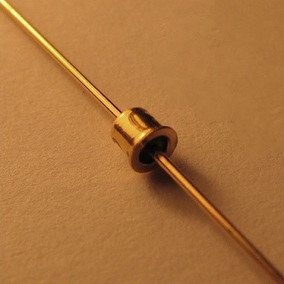
The following image shows how a practical tunnel diode looks like.
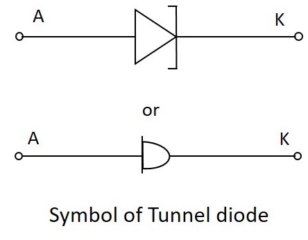
The symbols of tunnel diode are as shown below.
For more details regarding tunnel diodes, please refer our Basic Electronics tutorial.
Tunnel Diode Oscillator
The tunnel diode helps in generating a very high frequency signal of nearly 10GHz. A practical tunnel diode circuit may consist of a switch S, a resistor R and a supply source V, connected to a tank circuit through a tunnel diode D.
Working
The value of resistor selected should be in such a way that it biases the tunnel diode in the midway of the negative resistance region. The figure below shows the practical tunnel diode oscillator circuit.
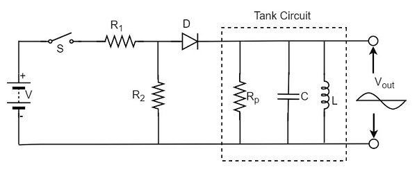
In this circuit, the resistor R1 sets proper biasing for the diode and the resistor R2 sets proper current level for the tank circuit. The parallel combination of resistor Rp inductor L and capacitor C form a tank circuit, which resonates at the selected frequency.
When the switch S is closed, the circuit current rises immediately towards the constant value, whose value is determined by the value of resistor R and the diode resistance. However, as the voltage drop across the tunnel diode VD exceeds the peak-point voltage Vp, the tunnel diode is driven into negative resistance region.
In this region, the current starts decreasing, till the voltage VD becomes equal to the valleypoint voltage Vv. At this point, a further increase in the voltage VD drives the diode into positive resistance region. As a result of this, the circuit current tends to increase. This increase in circuit will increase the voltage drop across the resistor R which will reduce the voltage VD.
V-I characteristic curve
The following graph shows the V-I characteristics of a tunnel diode −
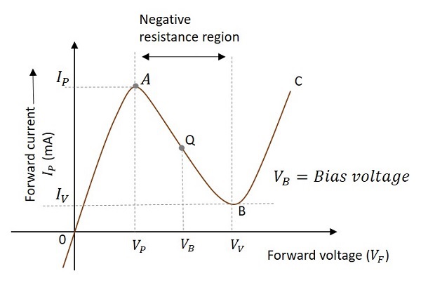
The curve AB indicates the negative resistance region as the resistance decreases while the voltage increases. It is clear that the Q-point is set at the middle of the curve AB. The Q-point can move between the points A and B during the circuit operation. The point A is called peak point and the point B is called valley point.
During the operation, after reaching the point B, the increase in circuit current will increase the voltage drop across the resistor R which will reduce the voltage VD. This brings the diode back into negative resistance region.
The decrease in voltage VD is equal to the voltage VP and this completes one cycle of operation. The continuation of these cycles produces continuous oscillations which give a sinusoidal output.
Advantages
The advantages of a tunnel diode oscillator are as follows −
- It has high switching speeds.
- It can handle high frequencies.
Disadvantages
The disadvantages of a tunnel diode oscillator are as follows −
- They are low power devices.
- Tunnel diodes are a bit costly.
Applications
The applications of a tunnel diode oscillator are as follows −
- It is used in relaxation oscillators.
- It is used in microwave oscillators.
- It is also used as Ultra high speed switching device.
- It is used as logic memory storage device.
After having covered all the major sinusoidal oscillator circuits, it is to be noted that there are many oscillators like the ones mentioned till now. The oscillators which produce sine waveforms are sinusoidal oscillators as discussed.
The oscillators which produce non-sinusoidal waveforms (rectangular, sweep, triangular etc.) are non-sinusoidal oscillators which we have discussed in detail in our Pulse Circuits tutorial.
To Continue Learning Please Login