- Digital Electronics - Home
- Digital Electronics Basics
- Types of Digital Systems
- Types of Signals
- Logic Levels And Pulse Waveforms
- Digital System Components
- Digital Logic Operations
- Digital Systems Advantages
- Number Systems
- Number Systems
- Binary Numbers Representation
- Binary Arithmetic
- Signed Binary Arithmetic
- Octal Arithmetic
- Hexadecimal Arithmetic
- Complement Arithmetic
- Base Conversions
- Base Conversions
- Binary to Decimal Conversion
- Decimal to Binary Conversion
- Binary to Octal Conversion
- Octal to Binary Conversion
- Octal to Decimal Conversion
- Decimal to Octal Conversion
- Hexadecimal to Binary Conversion
- Binary to Hexadecimal Conversion
- Hexadecimal to Decimal Conversion
- Decimal to Hexadecimal Conversion
- Octal to Hexadecimal Conversion
- Hexadecimal to Octal Conversion
- Binary Codes
- Binary Codes
- 8421 BCD Code
- Excess-3 Code
- Gray Code
- ASCII Codes
- EBCDIC Code
- Code Conversion
- Error Detection & Correction Codes
- Logic Gates
- Logic Gates
- AND Gate
- OR Gate
- NOT Gate
- Universal Gates
- XOR Gate
- XNOR Gate
- CMOS Logic Gate
- OR Gate Using Diode Resistor Logic
- AND Gate vs OR Gate
- Two Level Logic Realization
- Threshold Logic
- Boolean Algebra
- Boolean Algebra
- Laws of Boolean Algebra
- Boolean Functions
- DeMorgan's Theorem
- SOP and POS Form
- POS to Standard POS Form
- Minimization Techniques
- K-Map Minimization
- Three Variable K-Map
- Four Variable K-Map
- Five Variable K-Map
- Six Variable K-Map
- Don't Care Condition
- Quine-McCluskey Method
- Min Terms and Max Terms
- Canonical and Standard Form
- Max Term Representation
- Simplification using Boolean Algebra
- Combinational Logic Circuits
- Digital Combinational Circuits
- Digital Arithmetic Circuits
- Multiplexers
- Multiplexer Design Procedure
- Mux Universal Gate
- 2-Variable Function Using 4:1 Mux
- 3-Variable Function Using 8:1 Mux
- Demultiplexers
- Mux vs Demux
- Parity Bit Generator and Checker
- Comparators
- Encoders
- Keyboard Encoders
- Priority Encoders
- Decoders
- Arithmetic Logic Unit
- 7-Segment LED Display
- Code Converters
- Code Converters
- Binary to Decimal Converter
- Decimal to BCD Converter
- BCD to Decimal Converter
- Binary to Gray Code Converter
- Gray Code to Binary Converter
- BCD to Excess-3 Converter
- Excess-3 to BCD Converter
- Adders
- Half Adders
- Full Adders
- Serial Adders
- Parallel Adders
- Full Adder using Half Adder
- Half Adder vs Full Adder
- Full Adder with NAND Gates
- Half Adder with NAND Gates
- Binary Adder-Subtractor
- Subtractors
- Half Subtractors
- Full Subtractors
- Parallel Subtractors
- Full Subtractor using 2 Half Subtractors
- Half Subtractor using NAND Gates
- Sequential Logic Circuits
- Digital Sequential Circuits
- Clock Signal and Triggering
- Latches
- Shift Registers
- Shift Register Applications
- Binary Registers
- Bidirectional Shift Register
- Counters
- Binary Counters
- Non-binary Counter
- Design of Synchronous Counter
- Synchronous vs Asynchronous Counter
- Finite State Machines
- Algorithmic State Machines
- Flip Flops
- Flip-Flops
- Conversion of Flip-Flops
- D Flip-Flops
- JK Flip-Flops
- T Flip-Flops
- SR Flip-Flops
- Clocked SR Flip-Flop
- Unclocked SR Flip-Flop
- Clocked JK Flip-Flop
- JK to T Flip-Flop
- SR to JK Flip-Flop
- Triggering Methods:Flip-Flop
- Edge-Triggered Flip-Flop
- Master-Slave JK Flip-Flop
- Race-around Condition
- A/D and D/A Converters
- Analog-to-Digital Converter
- Digital-to-Analog Converter
- DAC and ADC ICs
- Realization of Logic Gates
- NOT Gate from NAND Gate
- OR Gate from NAND Gate
- AND Gate from NAND Gate
- NOR Gate from NAND Gate
- XOR Gate from NAND Gate
- XNOR Gate from NAND Gate
- NOT Gate from NOR Gate
- OR Gate from NOR Gate
- AND Gate from NOR Gate
- NAND Gate from NOR Gate
- XOR Gate from NOR Gate
- XNOR Gate from NOR Gate
- NAND/NOR Gate using CMOS
- Full Subtractor using NAND Gate
- AND Gate Using 2:1 MUX
- OR Gate Using 2:1 MUX
- NOT Gate Using 2:1 MUX
- Memory Devices
- Memory Devices
- RAM and ROM
- Cache Memory Design
- Programmable Logic Devices
- Programmable Logic Devices
- Programmable Logic Array
- Programmable Array Logic
- Field Programmable Gate Arrays
- Digital Electronics Families
- Digital Electronics Families
- CPU Architecture
- CPU Architecture
Multiplexer Design Procedure and Applications
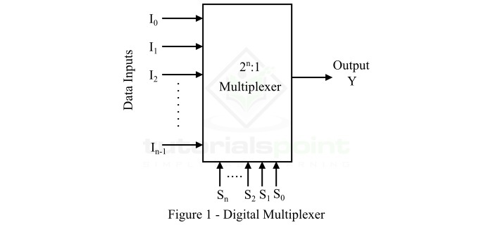
A multiplexer (MUX) is a digital combinational logic circuit that accepts multiple data inputs and allows only one of them at a time to transmit over an output channel. A multiplexer consists of 2n input lines, n select lines, and one output line. In a multiplexer, the routing of the desired data input to the output channel is done by the logic level applied to the select lines. The functional block diagram of a multiplexer is shown in Figure-1.
This chapter is primarily meant for explaining the design procedure of different types of multiplexer circuits. More specifically, here we will discuss the design procedure of the following three types of multiplexer −
- 2:1 Multiplexer
- 4:1 Multiplexer
- 8:1 Multiplexer
So let us now discuss the designing of each of these three types of multiplexer.
Designing a 2:1 Multiplexer
A 2:1 multiplexer (MUX) is one which has 2 input lines (I0 and I1), 1 select line (S), and 1 output line (Y). The logic level applied to the select line S determines which data input will pass through the output line.
For determining the Boolean expression for output (Y) of the 2:1 multiplexer and its logic circuit implementation, we first need its function table (truth table) that gives information about operation of the circuit. The function table of the 2:1 multiplexer with data input I0 and I1 is shown below.
| Select Line (S) | Output (Y) |
|---|---|
| 0 | I0 |
| 1 | I1 |
Using this truth table, we can write the logic expression for the output of 2:1 MUX as,
$$\mathrm{Y\:=\:\bar{S}I_{0} \: + \: SI_{1}}$$
To implement this logic expression, we require two AND gates, one NOT gate, and one OR gate. The logic circuit of the 2:1 MUX is shown in Figure-2.

Operation
This logic circuit of the 2:1 MUX shown in figure-2 will work as follows −
- When S = 0, the AND gate A is enabled and the AND gate B is disabled. Therefore, the output Y = I0.
- When S = 1, the AND gate A is disabled and the AND gate B is enabled. Therefore, the output Y = I1.
This is how, we can design a 2:1 multiplexer.
Designing a 4:1 Multiplexer
A 4:1 multiplexer (MUX) is the MUX which has 4 input lines (I0, I1, I2, and I3 ), 2 select line (S0 and S1), and 1 output line (Y). The logic levels applied to the select lines S0 and S1 determine which data input will transmit to the output line.
For determining the Boolean expression for output (Y) of the 4:1 multiplexer and its logic circuitry, we require its function table (truth table) that provides information about the operation of its circuit. The function table of the 4:1 multiplexer with data inputs I0, I1, I2, and I3 is given below.
| Select Lines | Output(Y) | |
|---|---|---|
| S1 | S0 | |
| 0 | 0 | I0 |
| 0 | 0 | I1 |
| 1 | 0 | I2 |
| 1 | 1 | I3 |
Using this truth table, we can write the logic expression for the output of 4:1 MUX as,
$$\mathrm{Y\:=\:\bar{S_{1}}\bar{S_{0}}I_{0}\:+\:\bar{S_{1}}S_{0}I_{1}\:+\:S_{1}\bar{S_{0}}I_{2}\:+\:S_{1}S_{0}I_{3}}$$
To implement this logic expression, we require four AND gates, two NOT gates, and one OR gate. Thus, the logic circuit of the 4:1 MUX is shown in Figure-3.
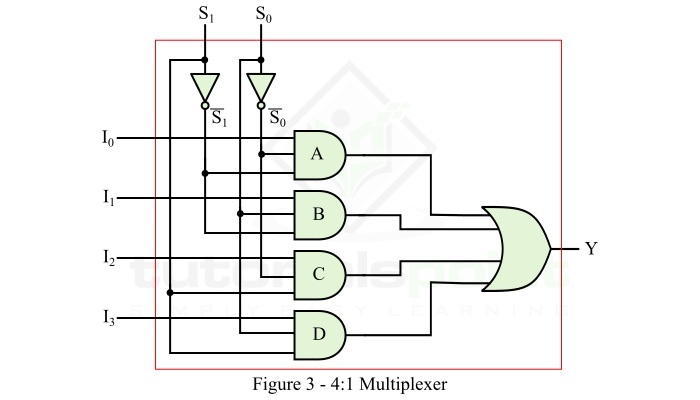
Operation
This logic circuit of the 4:1 MUX shown in Figure-3 will work as follows −
- When S1 = 0 and S0 = 0, the AND gate A is enabled, and the AND gates B, C, and D are disabled. So, the output Y = I0.
- When S1 = 0 and S0 = 1, the AND gate B is enabled, and the AND gates A, C, and D are disabled. So, the output Y = I1.
- When S1 = 1 and S0 = 0, the AND gate C is enabled, and the AND gates A, B, and D are disabled. So, the output Y = I2.
- When S1 = 1 and S0 = 1, the AND gate D is enabled, and the AND gates A, B, and C are disabled. So, the output Y = I3.
In this way, we can design a 4:1 multiplexer.
Design 8:1 Multiplexer
An 8:1 multiplexer (MUX) is a combination logic circuit which has 8 input lines (I0, I1, I2, I3, I4, I5, I6, and I7), 3 select line (S0, S1, and S2), and 1 output line (Y). The logic levels applied to the select lines S0, S1, and S2 determine which data input will transmit to the output line.
To determine the logic expression for output (Y) of the 8:1 multiplexer and its logic circuitry, we require its function table (truth table) which provides information about the operation of its logic circuit.
The function table of the 8:1 multiplexer with data inputs I0, I1, I2, I3, I4, I5, I6, and I7 and select lines, S0, S1, and S2 is given below.
| Select Lines | Output (Y) | ||
|---|---|---|---|
| S2 | S1 | S0 | |
| 0 | 0 | 0 | I0 |
| 0 | 0 | 1 | I1 |
| 0 | 1 | 0 | I2 |
| 0 | 1 | 1 | I3 |
| 1 | 0 | 0 | I4 |
| 1 | 0 | 1 | I5 |
| 1 | 1 | 0 | I6 |
| 1 | 1 | 1 | I7 |
By using this function table, we can write the logic expression for the output of 8:1 MUX as,
$$\mathrm{Y\:=\:\bar{S_{2}}\bar{S_{1}}\bar{S_{0}}I_{0}+\bar{S_{2}}\bar{S_{1}}S_{0}I_{1}+\bar{S_{2}}S_{1}\bar{S_{0}}I_{2}+\bar{S_{2}}S_{1}S_{0}I_{3}+S_{2}\bar{S_{1}}\bar{S_{0}}I_{4}+S_{2}\bar{S_{1}}S_{0}I_{5}+S_{2}S_{1}\bar{S_{0}}I_{6}+S_{2}S_{1}S_{0}I_{7}}$$
To implement this logic expression, we require eight AND gates, three NOT gates, and one OR gate. Therefore, the logic circuit of the 8:1 MUX is shown in Figure-4.
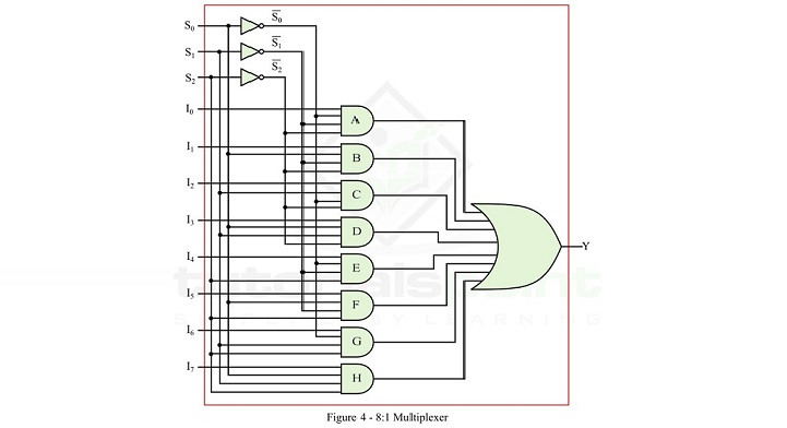
Operation
This logic circuit of the 8:1 MUX shown in Fgure-4 will operate as follows −
- When S2 = 0, S1 = 0, and S0 = 0, the AND gate A is enabled, and all the other AND gates in the logic circuit are disabled. So, the output Y = I0.
- When S2 = 0, S1 = 0, and S0 = 1, the AND gate B is enabled, and all the other AND gates in the logic circuit are disabled. So, the output Y = I1.
- When S2 = 0, S1 = 1, and S0 = 0, the AND gate C is enabled, and all the other AND gates in the logic circuit are disabled. So, the output Y = I2.
- When S2 = 0, S1 = 1, and S0 = 1, the AND gate D is enabled, and all the other AND gates in the logic circuit are disabled. So, the output Y = I3.
- When S2 = 1, S1 = 0, and S0 = 0, the AND gate E is enabled, and all the other AND gates in the logic circuit are disabled. So, the output Y = I4.
- When S2 = 1, S1 = 0, and S0 = 1, the AND gate F is enabled, and all the other AND gates in the logic circuit are disabled. So, the output Y = I5.
- When S2 = 1, S1 = 1, and S0 = 0, the AND gate G is enabled, and all the other AND gates in the logic circuit are disabled. So, the output Y = I6.
- When S2 = 1, S1 = 1, and S0 = 1, the AND gate H is enabled, and all the other AND gates in the logic circuit are disabled. So, the output Y = I7.
In this way, we can design an 8:1 multiplexer.
Applications of Multiplexers
The multiplexer is one of the widely combinational logic circuits in digital systems. Some important applications of the multiplexers are listed below.
- Multiplexer is used as data selector device.
- Multiplexers are used in communication systems to increase the efficiency of the system.
- Multiplexers are used in telephone networks for integration of several audio signals on a single transmission line.
- To maintain large amount of data, multiplexers are also used in computer memory systems.
- Multiplexers are also employed in TV broadcasting systems.
- Multiplexers are used in satellite communication and GPS (Global Positioning System).
- Multiplexers are also used in PLC (Programmable Logic Control) systems, etc.
This is all about the multiplexer design procedure, and applications of multiplexers.
