- Linear Wave Shapping
- Special Functions of LPF and HPF
- Nonlinear Wave Shapping
- Positive Clipper Circuits
- Negative Clipper Circuits
- Clamper Circuits
- Limiter & Voltage Multiplier
- Diode as a Switch
- Power Supplies
- Power Supplies
- Electronic Circuits - Rectifiers
- Full Wave Rectifiers
- Electronic Circuits - Filters
- Electronic Circuits - Regulators
- Electronic Circuits - SMPS
- Electronic Circuits Resources
- Electronic Circuits - Quick Guide
- Electronic Circuits - Resources
- Electronic Circuits - Discussion
Electronic Circuits - Full Wave Rectifiers
A Rectifier circuit that rectifies both the positive and negative half cycles can be termed as a full wave rectifier as it rectifies the complete cycle. The construction of a full wave rectifier can be made in two types. They are
- Center-tapped Full wave rectifier
- Bridge full wave rectifier
Both of them have their advantages and disadvantages. Let us now go through both of their construction and working along with their waveforms to know which one is better and why.
Center-tapped Full-Wave Rectifier
A rectifier circuit whose transformer secondary is tapped to get the desired output voltage, using two diodes alternatively, to rectify the complete cycle is called as a Center-tapped Full wave rectifier circuit. The transformer is center tapped here unlike the other cases.
The features of a center-tapping transformer are −
The tapping is done by drawing a lead at the mid-point on the secondary winding. This winding is split into two equal halves by doing so.
The voltage at the tapped mid-point is zero. This forms a neutral point.
The center tapping provides two separate output voltages which are equal in magnitude but opposite in polarity to each other.
A number of tapings can be drawn out to obtain different levels of voltages.
The center-tapped transformer with two rectifier diodes is used in the construction of a Center-tapped full wave rectifier. The circuit diagram of a center tapped full wave rectifier is as shown below.
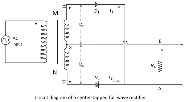
Working of a CT- FWR
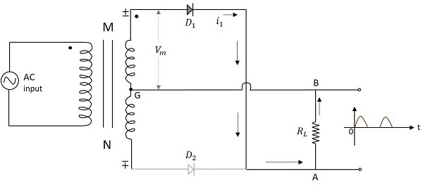
The working of a center-tapped full wave rectifier can be understood by the above figure. When the positive half cycle of the input voltage is applied, the point M at the transformer secondary becomes positive with respect to the point N. This makes the diode $D_1$forward biased. Hence current $i_1$ flows through the load resistor from A to B. We now have the positive half cycles in the output
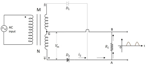
When the negative half cycle of the input voltage is applied, the point M at the transformer secondary becomes negative with respect to the point N. This makes the diode $D_2$ forward biased. Hence current $i_2$ flows through the load resistor from A to B. We now have the positive half cycles in the output, even during the negative half cycles of the input.
Waveforms of CT FWR
The input and output waveforms of the center-tapped full wave rectifier are as follows.
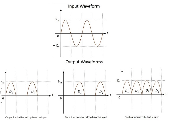
From the above figure it is evident that the output is obtained for both the positive and negative half cycles. It is also observed that the output across the load resistor is in the same direction for both the half cycles.
Peak Inverse Voltage
As the maximum voltage across half secondary winding is $V_m$, the whole of the secondary voltage appears across the non-conducting diode. Hence the peak inverse voltage is twice the maximum voltage across the half-secondary winding, i.e.
$$PIV=2V_m$$
Disadvantages
There are few disadvantages for a center-tapped full wave rectifier such as −
- Location of center-tapping is difficult
- The dc output voltage is small
- PIV of the diodes should be high
The next kind of full wave rectifier circuit is the Bridge Full wave rectifier circuit.
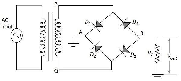
Bridge Full-Wave Rectifier
This is such a full wave rectifier circuit which utilizes four diodes connected in bridge form so as not only to produce the output during the full cycle of input, but also to eliminate the disadvantages of the center-tapped full wave rectifier circuit.
There is no need of any center-tapping of the transformer in this circuit. Four diodes called $D_1$, $D_2$, $D_3$ and $D_4$ are used in constructing a bridge type network so that two of the diodes conduct for one half cycle and two conduct for the other half cycle of the input supply. The circuit of a bridge full wave rectifier is as shown in the following figure.
Working of a Bridge Full-Wave Rectifier
The full wave rectifier with four diodes connected in bridge circuit is employed to get a better full wave output response. When the positive half cycle of the input supply is given, point P becomes positive with respect to the point Q. This makes the diode $D_1$ and $D_3$ forward biased while $D_2$ and $D_4$ reverse biased. These two diodes will now be in series with the load resistor.
The following figure indicates this along with the conventional current flow in the circuit.
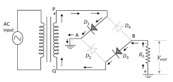
Hence the diodes $D_1$ and $D_3$ conduct during the positive half cycle of the input supply to produce the output along the load resistor. As two diodes work in order to produce the output, the voltage will be twice the output voltage of the center tapped full wave rectifier.
When the negative half cycle of the input supply is given, point P becomes negative with respect to the point Q. This makes the diode $D_1$ and $D_3$ reverse biased while $D_2$ and $D_4$ forward biased. These two diodes will now be in series with the load resistor.
The following figure indicates this along with the conventional current flow in the circuit.
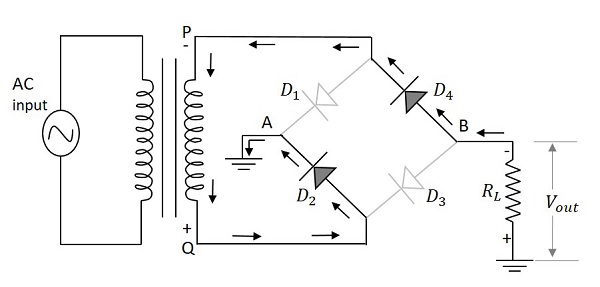
Hence the diodes $D_{2}$ and $D_{4}$ conduct during the negative half cycle of the input supply to produce the output along the load resistor. Here also two diodes work to produce the output voltage. The current flows in the same direction as during the positive half cycle of the input.
Waveforms of Bridge FWR
The input and output waveforms of the center-tapped full wave rectifier are as follows.
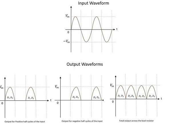
From the above figure, it is evident that the output is obtained for both the positive and negative half cycles. It is also observed that the output across the load resistor is in the same direction for both the half cycles.
Peak Inverse Voltage
Whenever two of the diodes are being in parallel to the secondary of the transformer, the maximum secondary voltage across the transformer appears at the non-conducting diodes which makes the PIV of the rectifier circuit. Hence the peak inverse voltage is the maximum voltage across the secondary winding, i.e.
$$PIV=V_m$$
Advantages
There are many advantages for a bridge full wave rectifier, such as −
- No need of center-tapping.
- The dc output voltage is twice that of the center-tapper FWR.
- PIV of the diodes is of the half value that of the center-tapper FWR.
- The design of the circuit is easier with better output.
Let us now analyze the characteristics of a full-wave rectifier.
Analysis of Full-Wave Rectifier
In order to analyze a full wave rectifier circuit, let us assume the input voltage $V_{i}$ as,
$$V_{i}=V_m \sin \omega t$$
The current $i_1$ through the load resistor $R_L$ is given by
$$i_1=I_m \sin \omega t \quad for \quad0 \leq \omega t \leq \pi$$
$$i_1=\quad0 \quad\quad\quad for \quad \pi \leq \omega t \leq 2\pi$$
Where
$$I_m=\frac{V_m}{R_f+R_L}$$
$R_f$ being the diode resistance in ON condition.
Similarly, the current $i_2$ flowing through diode $D_2$ and load resistor RL is given by,
$$i_2=\quad\:0 \quad\quad\quad for \quad 0 \leq \omega t \leq \pi$$
$$i_2=I_m \sin \omega t \quad for \quad\pi \leq \omega t \leq 2\pi$$
The total current flowing through $R_L$ is the sum of the two currents $i_1$ and $i_2$ i.e.
$$i=i_1+i_2$$
D.C. or Average Current
The average value of output current that a D.C. ammeter will indicate is given by
$$I_{dc}=\frac{1}{2\pi} \int_{0}^{2\pi} i_1 \:d\left ( \omega t \right )+\frac{1}{2\pi}\int_{0}^{2\pi}i_2 \:d\left ( \omega t \right )$$
$$=\frac{1}{2\pi\int_{0}^{\pi}}I_m \sin \omega t \:d\left ( \omega t \right )+0+0+$$
$$\frac{1}{2\pi} \int_{0}^{2\pi}I_m \sin \omega t\:d\left ( \omega t \right ) $$
$$=\frac{I_m}{\pi}+ \frac{I_m}{\pi} =\frac{2I_m}{\pi}=0.636I_m$$
This is double the value of a half wave rectifier.
D.C. Output Voltage
The dc output voltage across load is given by
$$V_{dc}=I_{dc}\times R_L = \frac{2I_mR_L}{\pi}=0.636I_mR_L$$
Thus the dc output voltage is twice that of a half wave rectifier.
RMS Current
The RMS value of the current is given by
$$I_{rms}=\left [ \frac{1}{\pi}\int_{0}^{\pi} t^2 \:d\left ( \omega t \right )\right ]^{\frac{1}{2}}$$
Since current is of the two same form in the two halves
$$=\left [ \frac{I_{m}^{2}}{\pi} \int_{0}^{\pi }\sin^2 \omega t\:d\left ( \omega t \right )\right ]^{\frac{1}{2}}$$
$$=\frac{I_m}{\sqrt{2}}$$
Rectifier Efficiency
The rectifier efficiency is defined as
$$\eta=\frac{P_{dc}}{P_{ac}}$$
Now,
$$P_{dc}=\left (V_{dc} \right )^2/R_L=\left ( 2V_m/\pi \right )^2$$
And,
$$P_{ac}=\left (V_{rms} \right )^2/R_L=\left (V_m/\sqrt{2} \right )^2$$
Therefore,
$$\eta =\frac{P_{dc}}{P_{ac}}=\frac{\left (2V_m/\pi \right )^2}{\left ( V_m/\sqrt{2} \right )^2}=\frac{8}{\pi^2}$$
$$=0.812=81.2\%$$
The rectifier efficiency can be calculated as follows −
The dc output power,
$$P_{dc}=I_{dc}^{2}R_L=\frac{4I_{m}^{2}}{\pi^2}\times R_L$$
The ac input power,
$$P_{ac}=I_{rms}^{2}\left (R_f+R_L \right )=\frac{I_{m}^{2}}{2}\left ( R_f+R_L \right )$$
Therefore,
$$\eta=\frac{4I_{m}^{2}R_L/\pi^2}{I_{m}^{2}\left ( R_f+R_L \right )/2}=\frac{8}{\pi^2}\frac{R_L}{\left ( R_f+R_L \right )}$$
$$=\frac{0.812}{\left \{ 1+\left ( R_f/R_L \right ) \right \}}$$
Therefore, Percentage Efficiency is
$$=\frac{0.812}{ 1+\left ( R_f+R_L \right )}$$
$$=81.2\% \quad if\: R_f=0$$
Thus, a full-wave rectifier has efficiency twice that of half wave rectifier.
Ripple Factor
The form factor of rectified output voltage of a full wave rectifier is given by
$$F=\frac{I_{rms}}{I_{dc}}=\frac{I_m/\sqrt{2}}{2I_m/\pi}=1.11$$
The ripple factor $\gamma$ is defined as (using ac circuit theory)
$$\gamma =\left [ \left ( \frac{I_{rms}}{I_{dc}} \right )-1 \right ]^{\frac{1}{2}}=\left ( F^2 -1\right )^{\frac{1}{2}}$$
$$=\left [ \left ( 1.11 \right )^2 -1\right ]^\frac{1}{2}=0.48$$
This is a great improvement over the half wave rectifiers ripple factor which was 1.21
Regulation
The dc output voltage is given by
$$V_{dc}=\frac{2I_mR_L}{\pi}=\frac{2V_mR_L}{\pi\left ( R_f+R_L \right )}$$
$$=\frac{2V_m}{\pi}\left [ 1-\frac{R_f}{R_f+R_L} \right ]=\frac{2V_m}{\pi}-I_{dc}R_f$$
Transformer Utilization Factor
The TUF of a half wave rectifier is 0.287
There are two secondary windings in a center-tapped rectifier and hence the TUF of centertapped full wave rectifier is
$$\left ( TUF \right )_{avg}=\frac{P_{dc}}{V-A\:rating\:of\:a\:transformer}$$
$$=\frac{\left ( TUF \right )_p+\left ( TUF \right )_s+\left ( TUF \right )_s}{3}$$
$$=\frac{0.812+0.287+0.287}{3}=0.693$$
Half-Wave vs. Full-Wave Rectifier
After having gone through all the values of different parameters of the full wave rectifier, let us just try to compare and contrast the features of half-wave and full-wave rectifiers.
| Terms | Half Wave Rectifier | Center Tapped FWR | Bridge FWR |
|---|---|---|---|
| Number of Diodes | $1$ | $2$ | $4$ |
| Transformer tapping | $No$ | $Yes$ | $No$ |
| Peak Inverse Voltage | $V_m$ | $2V_m$ | $V_m$ |
| Maximum Efficiency | $40.6\%$ | $81.2\%$ | $81.2\%$ |
| Average / dc current | $I_m/\pi$ | $2I_m/\pi$ | $2I_m/\pi$ |
| DC voltage | $V_m/\pi$ | $2V_m/\pi$ | $2V_m/\pi$ |
| RMS current | $I_m/2$ | $I_m/\sqrt{2}$ | $I_m/\sqrt{2}$ |
| Ripple Factor | $1.21$ | $0.48$ | $0.48$ |
| Output frequency | $f_{in}$ | $2f_{in}$ | $2f_{in}$ |
