- ES - Home
- ES - Overview
- ES - Processors
- ES - Architectures
- ES - Tools and Peripherals
- ES - 8051 Microcontroller
- ES - I/O Programming
- ES - Terms
- ES - Assembly Language
- ES - Registers
- ES - Registers Bank/Stack
- ES - Instructions
- ES - Addressing Modes
- ES - Special Function Registers
- ES - Timer/Counter
- ES - Interrupts
Embedded Systems - I/O Programming
In 8051, I/O operations are done using four ports and 40 pins. The following pin diagram shows the details of the 40 pins. I/O operation port reserves 32 pins where each port has 8 pins. The other 8 pins are designated as Vcc, GND, XTAL1, XTAL2, RST, EA (bar), ALE/PROG (bar), and PSEN (bar).
It is a 40 Pin PDIP (Plastic Dual Inline Package)
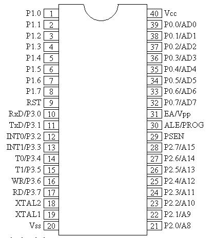
Note − In a DIP package, you can recognize the first pin and the last pin by the cut at the middle of the IC. The first pin is on the left of this cut mark and the last pin (i.e. the 40th pin in this case) is to the right of the cut mark.
I/O Ports and their Functions
The four ports P0, P1, P2, and P3, each use 8 pins, making them 8-bit ports. Upon RESET, all the ports are configured as inputs, ready to be used as input ports. When the first 0 is written to a port, it becomes an output. To reconfigure it as an input, a 1 must be sent to a port.
Port 0 (Pin No 32 Pin No 39)
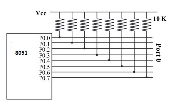
It has 8 pins (32 to 39). It can be used for input or output. Unlike P1, P2, and P3 ports, we normally connect P0 to 10K-ohm pull-up resistors to use it as an input or output port being an open drain.
It is also designated as AD0-AD7, allowing it to be used as both address and data. In case of 8031 (i.e. ROMless Chip), when we need to access the external ROM, then P0 will be used for both Address and Data Bus. ALE (Pin no 31) indicates if P0 has address or data. When ALE = 0, it provides data D0-D7, but when ALE = 1, it has address A0-A7. In case no external memory connection is available, P0 must be connected externally to a 10K-ohm pull-up resistor.
MOV A,#0FFH  ;(comments: A=FFH(Hexadecimal  i.e. A=1111 1111)

MOV P0,A     ;(Port0 have 1's on every pin so that it works as Input)
Port 1 (Pin 1 through 8)
It is an 8-bit port (pin 1 through 8) and can be used either as input or output. It doesn't require pull-up resistors because they are already connected internally. Upon reset, Port 1 is configured as an input port. The following code can be used to send alternating values of 55H and AAH to Port 1.
;Toggle all bits of continuously
MOV     A,#55
BACK:

MOV     P2,A
ACALL   DELAY
CPL     A      ;complement(invert) reg. A
SJMP    BACK
If Port 1 is configured to be used as an output port, then to use it as an input port again, program it by writing 1 to all of its bits as in the following code.
;Toggle all bits of continuously

MOV     A ,#0FFH    ;A = FF hex
MOV     P1,A        ;Make P1 an input port
MOV     A,P1        ;get data from P1
MOV     R7,A        ;save it in Reg R7
ACALL   DELAY       ;wait

MOV     A,P1        ;get another data from P1
MOV     R6,A        ;save it in R6
ACALL   DELAY       ;wait

MOV     A,P1        ;get another data from P1
MOV     R5,A        ;save it in R5
Port 2 (Pins 21 through 28)
Port 2 occupies a total of 8 pins (pins 21 through 28) and can be used for both input and output operations. Just as P1 (Port 1), P2 also doesn't require external Pull-up resistors because they are already connected internally. It must be used along with P0 to provide the 16-bit address for the external memory. So it is also designated as (A0A7), as shown in the pin diagram. When the 8051 is connected to an external memory, it provides path for upper 8-bits of 16-bits address, and it cannot be used as I/O. Upon reset, Port 2 is configured as an input port. The following code can be used to send alternating values of 55H and AAH to port 2.
;Toggle all bits of continuously
MOV     A,#55
BACK:
MOV     P2,A
ACALL   DELAY
CPL     A         ; complement(invert) reg. A
SJMP    BACK
If Port 2 is configured to be used as an output port, then to use it as an input port again, program it by writing 1 to all of its bits as in the following code.
;Get a byte from P2 and send it to P1
MOV    A,#0FFH    ;A = FF hex
MOV    P2,A       ;make P2 an input port
BACK:
MOV    A,P2       ;get data from P2
MOV    P1,A       ;send it to Port 1
SJMP   BACK       ;keep doing that
Port 3 (Pins 10 through 17)
It is also of 8 bits and can be used as Input/Output. This port provides some extremely important signals. P3.0 and P3.1 are RxD (Receiver) and TxD (Transmitter) respectively and are collectively used for Serial Communication. P3.2 and P3.3 pins are used for external interrupts. P3.4 and P3.5 are used for timers T0 and T1 respectively. P3.6 and P3.7 are Write (WR) and Read (RD) pins. These are active low pins, means they will be active when 0 is given to them and these are used to provide Read and Write operations to External ROM in 8031 based systems.
| P3 Bit | Function | Pin |
|---|---|---|
| P3.0 | RxD | 10 |
| P3.1 < | TxD | 11 |
| P3.2 < | Complement of INT0 | 12 |
| P3.3 < | INT1 | 13 |
| P3.4 < | T0 | 14 |
| P3.5 < | T1 | 15 |
| P3.6 < | WR | 16 |
| P3.7 < | Complement of RD | 17 |
Dual Role of Port 0 and Port 2
Dual role of Port 0 − Port 0 is also designated as AD0AD7, as it can be used for both data and address handling. While connecting an 8051 to external memory, Port 0 can provide both address and data. The 8051 microcontroller then multiplexes the input as address or data in order to save pins.
Dual role of Port 2 − Besides working as I/O, Port P2 is also used to provide 16-bit address bus for external memory along with Port 0. Port P2 is also designated as (A8 A15), while Port 0 provides the lower 8-bits via A0A7. In other words, we can say that when an 8051 is connected to an external memory (ROM) which can be maximum up to 64KB and this is possible by 16 bit address bus because we know 216 = 64KB. Port2 is used for the upper 8-bit of the 16 bits address, and it cannot be used for I/O and this is the way any Program code of external ROM is addressed.
Hardware Connection of Pins
Vcc − Pin 40 provides supply to the Chip and it is +5 V.
Gnd − Pin 20 provides ground for the Reference.
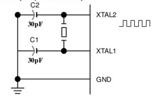
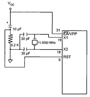
XTAL1, XTAL2 (Pin no 18 & Pin no 19) − 8051 has on-chip oscillator but requires external clock to run it. A quartz crystal is connected between the XTAL1 & XTAL2 pin of the chip. This crystal also needs two capacitors of 30pF for generating a signal of desired frequency. One side of each capacitor is connected to ground. 8051 IC is available in various speeds and it all depends on this Quartz crystal, for example, a 20 MHz microcontroller requires a crystal with a frequency no more than 20 MHz.
RST (Pin No. 9) − It is an Input pin and active High pin. Upon applying a high pulse on this pin, that is 1, the microcontroller will reset and terminate all activities. This process is known as Power-On Reset. Activating a power-on reset will cause all values in the register to be lost. It will set a program counter to all 0's. To ensure a valid input of Reset, the high pulse must be high for a minimum of two machine cycles before it is allowed to go low, which depends on the capacitor value and the rate at which it charges. (Machine Cycle is the minimum amount of frequency a single instruction requires in execution).
EA or External Access (Pin No. 31) − It is an input pin. This pin is an active low pin; upon applying a low pulse, it gets activated. In case of microcontroller (8051/52) having on-chip ROM, the EA (bar) pin is connected to Vcc. But in an 8031 microcontroller which does not have an on-chip ROM, the code is stored in an external ROM and then fetched by the microcontroller. In this case, we must connect the (pin no 31) EA to Gnd to indicate that the program code is stored externally.
PSEN or Program store Enable (Pin No 29) − This is also an active low pin, i.e., it gets activated after applying a low pulse. It is an output pin and used along with the EA pin in 8031 based (i.e. ROMLESS) Systems to allow storage of program code in external ROM.
ALE or (Address Latch Enable) − This is an Output Pin and is active high. It is especially used for 8031 IC to connect it to the external memory. It can be used while deciding whether P0 pins will be used as Address bus or Data bus. When ALE = 1, then the P0 pins work as Data bus and when ALE = 0, then the P0 pins act as Address bus.
I/O Ports and Bit Addressability
It is a most widely used feature of 8051 while writing code for 8051. Sometimes we need to access only 1 or 2 bits of the port instead of the entire 8-bits. 8051 provides the capability to access individual bits of the ports.
While accessing a port in a single-bit manner, we use the syntax "SETB X. Y" where X is the port number (0 to 3), and Y is a bit number (0 to 7) for data bits D0-D7 where D0 is the LSB and D7 is the MSB. For example, "SETB P1.5" sets high bit 5 of port 1.
The following code shows how we can toggle the bit P1.2 continuously.
AGAIN:
SETB    P1.2
ACALL   DELAY
CLR     P1.2
ACALL   DELAY
SJMP    AGAIN
Single-Bit Instructions
| Instructions | Function |
|---|---|
| SETB bit | Set the bit (bit = 1) |
| CLR bit | clear the bit (bit = 0) |
| CPL bit | complement the bit (bit = NOT bit) |
| JB bit, target | jump to target if bit = 1 (jump if bit) |
| JNB bit, target | jump to target if bit = 0 (jump if no bit) |
| JBC bit, target | jump to target if bit = 1, clear bit (jump if bit, then clear) |
