
- Semiconductor Devices - Home
- Introduction
- Atomic Combinations
- Conduction in Solid Materials
- Conductivity & Mobility
- Types of Semiconductor
- Doping in Semiconductors
- Junction Diodes
- Depletion Zone
- Barrier Potential
- Junction Biasing
- Leakage Current
- Diode Characteristics
- Light Emitting Diode
- Zener Diode
- Photo Diode
- Photovoltaic Cells
- Varactor Diode
- Bipolar Transistors
- Construction of a Transistor
- Transistor Biasing
- Configuration of Transistors
- Field Effect Transistors
- JFET Biasing
- Semiconductor Devices - MOSFET
- Operational Amplifiers
- Practical Op-Amps
- Semiconductor Devices - Integrator
- Differentiator
- Oscillators
- Feedback & Compensation
- Semiconductor Devices - Quick Guide
- Semiconductor Devices - Resources
- Semiconductor Devices - Discussion
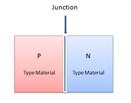
Semiconductor Devices - Junction Diodes
A crystal structure made of P and N materials is generally known as junction diode. It is generally regarded as a two-terminal device. As shown in the following diagram one terminal is attached to P-type material and the other to N-type material.
The common bond point where these materials are connected is called a junction. A junction diode allows current carriers to flow in one direction and obstruct the flow of current in the reverse direction.
The following figure shows the crystal structure of a junction diode. Take a look at the location of the P type and N type materials with respect to the junction. The structure of crystal is continuous from one end to the other. The junction acts only as a separating point that represents the end of one material and the beginning of the other. Such structure allows electrons to move thoroughly in the entire structure.
The following diagram shows two portions of semiconductor substance before they are shaped into a P-N junction. As specified, each part of material has majority and minority current carriers.
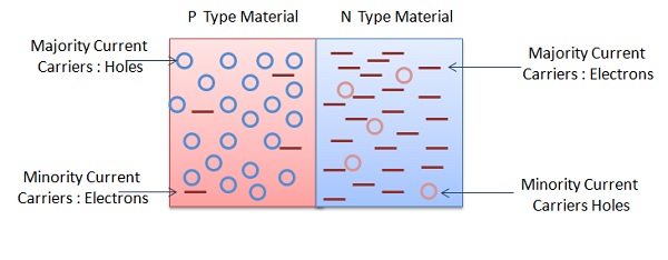
The quantity of carrier symbols shown in each material indicates the minority or majority function. As we know electrons are the majority carriers in the N type material and holes are the minority carriers. In P type material, holes are the majority carriers and electrons are in the minority.
