
- Microprocessor - Home
- Microprocessor Overview
- Microprocessor Classification
- Microprocessor Evolution
- Microprocessor Components
- Microprocessor Characteristics
- Microprocessor Functions
- Microprocessor Pros & Cons
- Microprocessor Application
- Microcontrollers Types
- Microcontrollers Pros & Cons
- 8085 Microprocessor Architecture
- 8085 Microprocessor Pin Configuration
- Addressing Modes & Interrupts
- 8085 Microprocessor Instruction Sets
- 8085 Microprocessor Features
- Externally Initiated Operations
- 8086 Microprocessor
- 8086 Microprocessor Overview
- Functional Units
- Pin Configuration
- Instruction Sets
- 8086 Microprocessor Interrupts
- 8086 Microprocessor Addressing Modes
- 8086 Microprocessor Features
- Memory Segmentation
- Auxiliary Carry Flag
- Maximum and Minimum Mode Configurations
- Multiprocessor Configuration
- Configuration Overview
- 8087 Numeric Data Processor
- I/O Interfacing
- I/O Interfacing Overview
- 8279 Programmable Keyboard
- 8257 DMA Controller
- Serial vs Parallel Communication
- Serial Communications Interface
- Parallel Communication Interface
- 8051 Microcontrollers
- Microcontrollers Overview
- 8051 Microcontrollers Architecture
- 8051 Pin Description
- 8051 Input Output Ports
- 8051 Microcontrollers Interrupts
- Instruction Sets
- Logical Instructions in AVR
- Conditional Branch Instructions AVR
- Arithmetic Instructions in AVR
- External Memory Interfacing
- Time Delay in AVR
- 8051 vs PIC Microcontroller
- Peripheral Devices
- Peripheral Devices
- Programmable Peripheral Interface
- Intel 8255A Pin Description
- Programmable Interval Timer
- 8253/54 Operational Modes
- Interfacing Devices
- Applications and Furture Trends
- Microcontrollers - Application
- Microprocessors and Microcontrollers in IoT
- Microcontrollers in Automotive Systems
- Microcontrollers - Low-Power
- Artificial Intelligence Processors
- Microprocessor Useful Resources
- Microprocessor - Quick Guide
- Microprocessor - Useful Resources
- Microprocessor - Discussion
Intel 8253 - Programmable Interval Timer
The Intel 8253 and 8254 are Programmable Interval Timers (PTIs) designed for microprocessors to perform timing and counting functions using three 16-bit registers. Each counter has 2 input pins, i.e. Clock & Gate, and 1 pin for OUT output. To operate a counter, a 16-bit count is loaded in its register. On command, it begins to decrement the count until it reaches 0, then it generates a pulse that can be used to interrupt the CPU.
Difference between 8253 and 8254
The following table differentiates the features of 8253 and 8254 −
| 8253 | 8254 |
|---|---|
| Its operating frequency is 0 - 2.6 MHz | Its operating frequency is 0 - 10 MHz |
| It uses N-MOS technology | It uses H-MOS technology |
| Read-Back command is not available | Read-Back command is available |
| Reads and writes of the same counter cannot be interleaved. | Reads and writes of the same counter can be interleaved. |
Features of 8253 / 54
The most prominent features of 8253/54 are as follows −
It has three independent 16-bit down counters.
It can handle inputs from DC to 10 MHz.
These three counters can be programmed for either binary or BCD count.
It is compatible with almost all microprocessors.
8254 has a powerful command called READ BACK command, which allows the user to check the count value, the programmed mode, the current mode, and the current status of the counter.
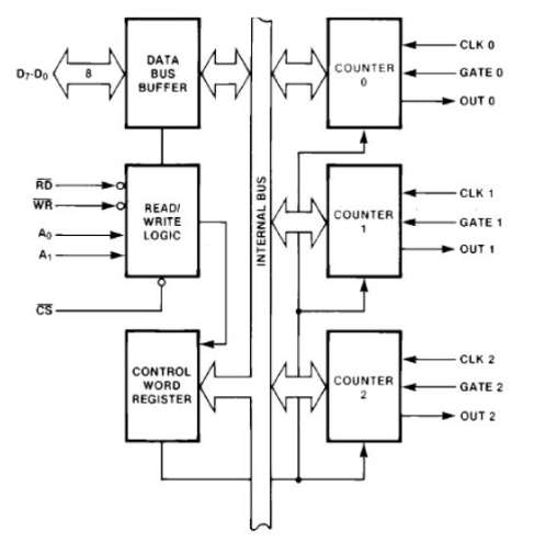
8254 Architecture
The architecture of 8254 looks as follows −
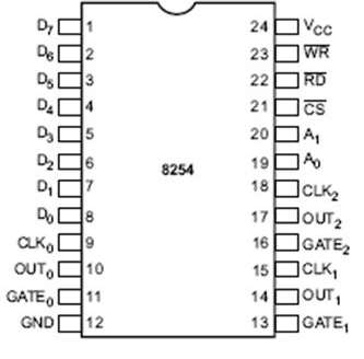
8254 Pin Description
Here is the pin diagram of 8254 −
In the above figure, there are three counters, a data bus buffer, Read/Write control logic, and a control register. Each counter has two input signals - CLOCK & GATE, and one output signal - OUT.
Data Bus Buffer
It is a tri-state, bi-directional, 8-bit buffer, which is used to interface the 8253/54 to the system data bus. It has three basic functions −
- Programming the modes of 8253/54.
- Loading the count registers.
- Reading the count values.
Read/Write Logic
It includes 5 signals, i.e. RD, WR, CS, and the address lines A0 & A1. In the peripheral I/O mode, the RD and WR signals are connected to IOR and IOW, respectively. In the memorymapped I/O mode, these are connected to MEMR and MEMW.
Address lines A0 & A1 of the CPU are connected to lines A0 and A1 of the 8253/54, and CS is tied to a decoded address. The control word register and counters are selected according to the signals on lines A0 & A1.
| A1 | A0 | Result |
|---|---|---|
| 0 | 0 | Counter 0 |
| 0 | 1 | Counter 1 |
| 1 | 0 | Counter 2 |
| 1 | 1 | Control Word Register |
| X | X | No Selection |
Control Word Register
This register is accessed when lines A0 & A1 are at logic 1. It is used to write a command word, which specifies the counter to be used, its mode, and either a read or write operation. Following table shows the result for various control inputs.
| A1 | A0 | RD | WR | CS | Result |
|---|---|---|---|---|---|
| 0 | 0 | 1 | 0 | 0 | Write Counter 0 |
| 0 | 1 | 1 | 0 | 0 | Write Counter 1 |
| 1 | 0 | 1 | 0 | 0 | Write Counter 2 |
| 1 | 1 | 1 | 0 | 0 | Write Control Word |
| 0 | 0 | 0 | 1 | 0 | Read Counter 0 |
| 0 | 1 | 0 | 1 | 0 | Read Counter 1 |
| 1 | 0 | 0 | 1 | 0 | Read Counter 2 |
| 1 | 1 | 0 | 1 | 0 | No operation |
| X | X | 1 | 1 | 0 | No operation |
| X | X | X | X | 1 | No operation |
Counters
Each counter consists of a single, 16 bit-down counter, which can be operated in either binary or BCD. Its input and output is configured by the selection of modes stored in the control word register. The programmer can read the contents of any of the three counters without disturbing the actual count in process.
