
- Microprocessor - Home
- Microprocessor Overview
- Microprocessor Classification
- Microprocessor Evolution
- Microprocessor Components
- Microprocessor Characteristics
- Microprocessor Functions
- Microprocessor Pros & Cons
- Microprocessor Application
- Microcontrollers Types
- Microcontrollers Pros & Cons
- 8085 Microprocessor Architecture
- 8085 Microprocessor Pin Configuration
- Addressing Modes & Interrupts
- 8085 Microprocessor Instruction Sets
- 8085 Microprocessor Features
- Externally Initiated Operations
- 8086 Microprocessor
- 8086 Microprocessor Overview
- Functional Units
- Pin Configuration
- Instruction Sets
- 8086 Microprocessor Interrupts
- 8086 Microprocessor Addressing Modes
- 8086 Microprocessor Features
- Memory Segmentation
- Auxiliary Carry Flag
- Maximum and Minimum Mode Configurations
- Multiprocessor Configuration
- Configuration Overview
- 8087 Numeric Data Processor
- I/O Interfacing
- I/O Interfacing Overview
- 8279 Programmable Keyboard
- 8257 DMA Controller
- Serial vs Parallel Communication
- Serial Communications Interface
- Parallel Communication Interface
- 8051 Microcontrollers
- Microcontrollers Overview
- 8051 Microcontrollers Architecture
- 8051 Pin Description
- 8051 Input Output Ports
- 8051 Microcontrollers Interrupts
- Instruction Sets
- Logical Instructions in AVR
- Conditional Branch Instructions AVR
- Arithmetic Instructions in AVR
- External Memory Interfacing
- Time Delay in AVR
- 8051 vs PIC Microcontroller
- Peripheral Devices
- Peripheral Devices
- Programmable Peripheral Interface
- Intel 8255A Pin Description
- Programmable Interval Timer
- 8253/54 Operational Modes
- Interfacing Devices
- Applications and Furture Trends
- Microcontrollers - Application
- Microprocessors and Microcontrollers in IoT
- Microcontrollers in Automotive Systems
- Microcontrollers - Low-Power
- Artificial Intelligence Processors
- Microprocessor Useful Resources
- Microprocessor - Quick Guide
- Microprocessor - Useful Resources
- Microprocessor - Discussion
Intel 8255A - Pin Description
Let us first take a look at the pin diagram of Intel 8255A −
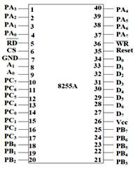
Now let us discuss the functional description of the pins in 8255A.
Data Bus Buffer
It is a tri-state 8-bit buffer, which is used to interface the microprocessor to the system data bus. Data is transmitted or received by the buffer as per the instructions by the CPU. Control words and status information is also transferred using this bus.
Read/Write Control Logic
This block is responsible for controlling the internal/external transfer of data/control/status word. It accepts the input from the CPU address and control buses, and in turn issues command to both the control groups.
CS
It stands for Chip Select. A LOW on this input selects the chip and enables the communication between the 8255A and the CPU. It is connected to the decoded address, and A0 & A1 are connected to the microprocessor address lines.
Their result depends on the following conditions −
| CS | A1 | A0 | Result |
|---|---|---|---|
| 0 | 0 | 0 | PORT A |
| 0 | 0 | 1 | PORT B |
| 0 | 1 | 0 | PORT C |
| 0 | 1 | 1 | Control Register |
| 1 | X | X | No Selection |
WR
It stands for write. This control signal enables the write operation. When this signal goes low, the microprocessor writes into a selected I/O port or control register.
RESET
This is an active high signal. It clears the control register and sets all ports in the input mode.
RD
It stands for Read. This control signal enables the Read operation. When the signal is low, the microprocessor reads the data from the selected I/O port of the 8255.
A0 and A1
These input signals work with RD, WR, and one of the control signal. Following is the table showing their various signals with their result.
| A1 | A0 | RD | WR | CS | Result |
|---|---|---|---|---|---|
| 0 | 0 | 0 | 1 | 0 | Input Operation PORT A → Data Bus |
| 0 | 1 | 0 | 1 | 0 | PORT B → Data Bus |
| 1 | 0 | 0 | 1 | 0 | PORT C → Data Bus |
| 0 | 0 | 1 | 0 | 0 | Output Operation Data Bus → PORT A |
| 0 | 1 | 1 | 0 | 0 | Data Bus → PORT A |
| 1 | 0 | 1 | 0 | 0 | Data Bus → PORT B |
| 1 | 1 | 1 | 0 | 0 | Data Bus → PORT D |
