
- Microprocessor - Home
- Microprocessor Overview
- Microprocessor Classification
- Microprocessor Evolution
- Microprocessor Components
- Microprocessor Characteristics
- Microprocessor Functions
- Microprocessor Pros & Cons
- Microprocessor Application
- Microcontrollers Types
- Microcontrollers Pros & Cons
- 8085 Microprocessor Architecture
- 8085 Microprocessor Pin Configuration
- Addressing Modes & Interrupts
- 8085 Microprocessor Instruction Sets
- 8085 Microprocessor Features
- Externally Initiated Operations
- 8086 Microprocessor
- 8086 Microprocessor Overview
- Functional Units
- Pin Configuration
- Instruction Sets
- 8086 Microprocessor Interrupts
- 8086 Microprocessor Addressing Modes
- 8086 Microprocessor Features
- Memory Segmentation
- Auxiliary Carry Flag
- Maximum and Minimum Mode Configurations
- Multiprocessor Configuration
- Configuration Overview
- 8087 Numeric Data Processor
- I/O Interfacing
- I/O Interfacing Overview
- 8279 Programmable Keyboard
- 8257 DMA Controller
- Serial vs Parallel Communication
- Serial Communications Interface
- Parallel Communication Interface
- 8051 Microcontrollers
- Microcontrollers Overview
- 8051 Microcontrollers Architecture
- 8051 Pin Description
- 8051 Input Output Ports
- 8051 Microcontrollers Interrupts
- Instruction Sets
- Logical Instructions in AVR
- Conditional Branch Instructions AVR
- Arithmetic Instructions in AVR
- External Memory Interfacing
- Time Delay in AVR
- 8051 vs PIC Microcontroller
- Peripheral Devices
- Peripheral Devices
- Programmable Peripheral Interface
- Intel 8255A Pin Description
- Programmable Interval Timer
- 8253/54 Operational Modes
- Interfacing Devices
- Applications and Furture Trends
- Microcontrollers - Application
- Microprocessors and Microcontrollers in IoT
- Microcontrollers in Automotive Systems
- Microcontrollers - Low-Power
- Artificial Intelligence Processors
- Microprocessor Useful Resources
- Microprocessor - Quick Guide
- Microprocessor - Useful Resources
- Microprocessor - Discussion
8087 Numeric Data Processor
8087 numeric data processor is also known as Math co-processor, Numeric processor extension and Floating point unit. It was the first math coprocessor designed by Intel to pair with 8086/8088 resulting in easier and faster calculation.
Once the instructions are identified by the 8086/8088 processor, then it is allotted to the 8087 co-processor for further execution.
The data types supported by 8087 are −
- Binary Integers
- Packed decimal numbers
- Real numbers
- Temporary real format
The most prominent features of 8087 numeric data processor are as follows −
It supports data of type integer, float, and real types ranging from 2-10 bytes.
The processing speed is so high that it can calculate multiplication of two 64-bits real numbers in ~27 s and can also calculate square-root in ~35 s.
It follows IEEE floating point standards.
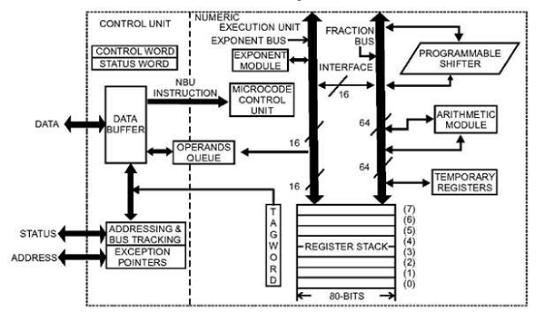
8087 Architecture
8087 Architecture is divided into two groups, i.e., Control Unit (CU) and Numeric Extension Unit (NEU).
The control unit handles all the communication between the processor and the memory such as it receives and decodes instructions, reads and writes memory operands, maintains parallel queue, etc. All the coprocessor instructions are ESC instructions, i.e., they start with F, the coprocessor only executes the ESC instructions while other instructions are executed by the microprocessor.
The numeric extension unit handles all the numeric processor instructions like arithmetic, logical, transcendental, and data transfer instructions. It has 8 register stack, which holds the operands for instructions and their results.
The architecture of 8087 coprocessor is as follows −
8087 Pin Description
Let us first take a look at the pin diagram of 8087 −
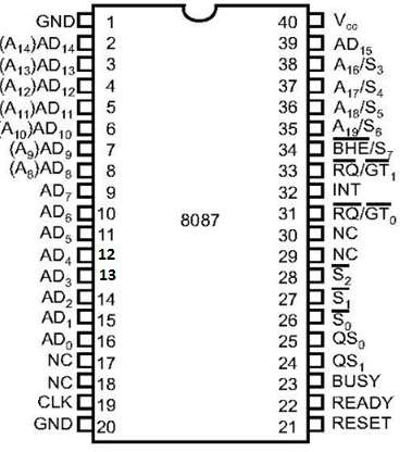
The following list provides the Pin Description of 8087 −
AD0 AD15 − These are the time multiplexed address/data lines, which carry addresses during the first clock cycle and data from the second clock cycle onwards.
A19 / S6 A16/S − These lines are the time multiplexed address/status lines. It functions in a similar way to the corresponding pins of 8086. The S6, S4 and S3 are permanently high, while the S5 is permanently low.
$\overline{BHE}$/S7 − During the first clock cycle, the $\overline{BHE}$/S7 is used to enable data on to the higher byte of the 8086 data bus and after that works as status line S7.
QS1, QS0 − These are queue status input signals which provides the status of instruction queue, their conditions as shown in the following table −
| QS0 | QS1 | Status |
|---|---|---|
| 0 | 0 | No operation |
| 0 | 1 | First byte of opcode from the queue |
| 1 | 0 | Empty the queue |
| 1 | 1 | Subsequent byte from the queue |
INT − It is an interrupt signal, which changes to high when an unmasked exception has been received during the execution.
BUSY − It is an output signal, when it is high it indicates a busy state to the CPU.
READY − It is an input signal used to inform the coprocessor whether the bus is ready to receive data or not.
RESET − It is an input signal used to reject the internal activities of the coprocessor and prepare it for further execution whenever required by the CPU.
CLK − The CLK input provides the basic timings for the processor operation.
VCC − It is a power supply signal, which requires +5V supply for the operation of the circuit.
S0, S1, S2 − These are the status signals that provide the status of the operation which is used by the Bus Controller 8087 to generate memory and I/O control signals. These signals are active during the fourth clock cycle.
| S2 | S1 | S0 | Queue Status |
|---|---|---|---|
| 0 | X | X | Unused |
| 1 | 0 | 0 | Unused |
| 1 | 0 | 1 | Memory read |
| 1 | 1 | 0 | Memory write |
| 1 | 1 | 1 | Passive |
RQ/GT1 & RQ/GT0 − These are the Request/Grant signals used by the 8087 processors to gain control of the bus from the host processor 8086/8088 for operand transfers.
