- Power Electronics - Home
- Power Electronics - Introduction
- Power Electronics - Switching Devices
- Linear Circuit Elements
- Power Electronics - Resistor
- Power Electronics - Inductor
- Power Electronics - Power Diode
- Power Diode - Reverse Recovery Characteristics
- Power Electronics - BJT
- Power Electronics - IGBT
- Power Electronics - MOSFET
- Silicon Controlled Rectifier
- SCR - Switching Characteristics
- Power Electronics - TRIAC
- Power Electronics - GTO Thyristor
- Comparision of Power Semiconductor Devices
- Thyristor - Diode Model
- Thyristor - Two Transistor Model
- Thyristor - Turn ON Methods
- Thyristor - Specifications and Ratings
- Solved Example
- Phase Controlled Converters
- Power Electronics - Pulse Converters
- Effect of Source Inductance
- Performance Parameters
- Reactive Power Control of Converters
- Power Electronics - Dual Converters
- Solved Example
- DC to DC Converters
- Power Electronics - Choppers
- Power Electronics - Control Methods
- Resonant Switching
- DC Converters Solved Example
- AC to DC Converters
- Single Phase AC Voltage Controllers
- Power Electronics - Cycloconverters
- Integral Cycle Control
- Power Electronics - Matrix Converters
- Solved Example
- Power Electronics Resources
- Power Electronics - Quick Guide
- Power Electronics - Useful Resources
- Power Electronics - Discussion
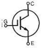
Power Electronics - IGBT
The insulated gate bipolar transistor (IGBT) is a semiconductor device with three terminals and is used mainly as an electronic switch. It is characterized by fast switching and high efficiency, which makes it a necessary component in modern appliances such as lamp ballasts, electric cars and variable frequency drives (VFDs).
Its ability to turn on and off, rapidly, makes it applicable in amplifiers to process complex wave-patterns with pulse width modulation. IGBT combines the characteristics of MOSFETs and BJTs to attain high current and low saturation voltage capacity respectively. It integrates an isolated gate using FET (Field effect transistor) to obtain a control input.
IGBT Symbol
The amplification of an IGBT is computed by the ratio of its output signal to its input signal. In conventional BJTs, the degree of gain (β) is equal to the ratio of its output current to the input current.
IGBT has a very low value of ON state resistance (RON) than a MOSFET. This implies that the voltage drop (I2R) across the bipolar for a particular switching operation is very low. The forward blocking action of the IGBT is similar to that of a MOSFET.
When an IGBT is used as controlled switch in a static state, its current and voltage ratings equal to that of BJT. On the contrary, the isolated gate in IGBT makes it easier to drive BJT charges and hence less power is required.
IGBT is switched ON or OFF based on whether its gate terminal has been activated or deactivated. A constant positive potential difference across the gate and the emitter maintains the IGBT in the ON state. When the input signal is removed, the IGBT is turned OFF.
IGBT Principle of Operation
IGBT requires only a small voltage to maintain conduction in the device unlike in BJT. The IGBT is a unidirectional device, that is, it can only switch ON in the forward direction. This means current flows from the collector to the emitter unlike in MOSFETs, which are bi-directional.
Applications of IGBT
The IGBT is used in medium to ultra-high power applications, for example traction motor. In large IGBT, it is possible to handle high current in the range of hundred amperes and blocking voltages of up to 6kv.
IGBTs are also used in power electronic devices such as converters, inverters and other appliances where the need for solid state switching is necessary. Bipolars are available with high current and voltage. However, their switching speeds are low. On the contrary, MOSFETs have high switching speeds although they are expensive.