
Article Categories
- All Categories
-
 Data Structure
-
 Networking
-
 RDBMS
RDBMS
-
 Operating System
-
 Java
Java
-
 MS Excel
-
 iOS
iOS
-
 HTML
HTML
-
 CSS
CSS
-
 Android
-
 Python
-
 C Programming
-
 C++
C++
-
 C#
C#
-
 MongoDB
-
 MySQL
MySQL
-
 Javascript
-
 PHP
PHP
-
 Economics & Finance
BiCMOS Technology: Fabrication Process and Applications
BiCMOS stands for Bipolar Complementary Metal-Oxide Semiconductor. BiCMOS technology is an integration technology that combines bipolar and CMOS (Complementary Metal Oxide Semiconductor) devices on a single chip. This technology is primarily used to combine the features of analog and digital circuits in a single IC chip.
In this article, we will discuss BiCMOS technology, its definition, fabrication process, advantages, disadvantages, and applications. Before discussing the BiCMOS technology, let us first get an overview of bipolar technology and CMOS technology individually.
What is Bipolar Technology?
A semiconductor technology in which BJTs (Bipolar Junction Transistors) are used as the fundamental building blocks of integrated circuits and other electronic devices is known as Bipolar Technology.
In bipolar devices, both majority and minority charge carriers control the flow of electric current. Bipolar junction transistors are three-terminal two pn-junction semiconductor devices that can be operated in three modes namely, active mode, saturation mode, and cut-off mode.
In the active mode, the bipolar junction transistor is biased to allow amplifying electric signals. In the saturation mode, the BJT is biased to allow a controlled flow of electric current between the emitter and the collector terminals. In the cutoff mode, the BJT is biased to cease the flow of electric current between the emitter and the collector terminal.
Bipolar technology is better in terms of current handling capacity, precisely controlled flow of the current, and high-frequency performance. Hence, bipolar devices are widely used in analog and power applications. However, it is less suitable for digital logic applications due to its high-power consumption and low switching speed.
What is CMOS Technology?
CMOS stands for Complementary Metal Oxide Semiconductor. CMOS is an IC (Integrated Circuit) manufacturing technology which is widely used to manufacture digital ICs, logic circuits, processors, memory chips, etc.
CMOS technology uses both N-channel and P-channel MOSFETs (Metal Oxide Field Effect Transistors) instead of BJTs. The n-channel MOSFETs and p-channel MOSFETs can operate in a complementary manner to perform logical operations.
CMOS technology offers several advantages over bipolar technology, including low power consumption, higher compatibility, high noise immunity, high efficiency, faster switching speed, etc. All these characteristics of CMOS technology make it suitable for digital logic circuits.
What is BiCMOS Technology?
BiCMOS is a semiconductor manufacturing technology that combines the advantages of both bipolar technology and CMOS (Complementary Metal Oxide Semiconductor) technology in a single chip.
BiCMOS is basically an integrated circuit manufacturing technology which uses a combination of BJTs and MOSFETs in a single integrated circuit. Therefore, BiCMOS allows integrating the analog and digital circuits on a single integrated circuit chip.
The combination of bipolar and CMOS technologies on a single chip provides high-switching speed, high current capabilities, low power consumption, etc. BiCMOS technology allows manufacturers to design mixed-signal ICs that handle both analog and digital signals efficiently. This technology significantly reduces the chip size with enhanced performance.
Therefore, BiCMOS ICs are extensively used in a variety of analog and digital electronic applications, like high-speed switches, automotive electronics, data converters, wireless and digital communication systems, and more.
Overall, BiCMOS technology is an advanced semiconductor manufacturing technology that integrates the advantages of bipolar technology and CMOS technology on a single IC chip. Hence, it is widely used in applications that require mixed signal functionalities.
BiCMOS Fabrication Process
The actual fabrication process of BiCMOS ICs generally varies depending on the fabrication facility and can be more complex. But a general fabrication process for BiCMOS ICs involves the following steps ?
Step 1 ? Prepare a semiconductor substrate (usually made up of silicon) by thoroughly cleaning it to remove all impurities and contaminations.
Step 2 ? Deposit a thin layer of epitaxial material on the top of the substrate to improve the electrical characteristics and performance of the device.
Step 3 ? Deposit a metal oxide layer (SiO2) on the surface of the substrate. This oxide layer provides insulation between different layers and components of the chip.
-
Step 4 ? Perform Photolithography. This process involves the following steps ?
Photoresist, a photosensitive material, is applied to the metal oxide layer.
A photomask that contains the desired circuitry patterns of the IC is placed over the substrate.
The ultraviolet light is made to pass through the photomask to expose the photoresist.
This will create the circuitry pattern on the chip.
Step 5 ? A chemical etching process is used to remove the exposed or unexposed areas of the photoresist. This process transfers the circuitry patterns from the photoresist onto the metal oxide layer.
Step 6 ? This step involves the creation of different regions of the bipolar and CMOS devices through dopant implantation. In this process, different dopant atoms are implanted into the substrate to create p-type and n-type regions.
Step 7 ? This step involves the thermal annealing of the substrate. In this process, the substrate is subjected to high temperatures that activate the dopants and repair any damages that occurred during the process of ion implantation.
Step 8 ? This step involves the metal deposition to create connections among different components on the chip. In this process, metal layers of copper or aluminum are deposited on the silicon substrate.
Step 9 ? In this step, insulating layers, usually of SiO2, are deposited on top of the metal layers.
Step 10 ? After completion of the fabrication process, the individual chips are tested for functionality and are encapsulated in a protective housing with connection pins/leads.
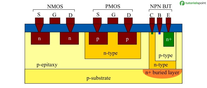
The final outcome of the above ten steps is illustrated in the figure shown below ?
Advantages of BiCMOS Technology
BiCMOS technology offers several advantages by combining bipolar and CMOS technology together. Some key benefits of the BiCMOS technology are listed below ?
BiCMOS technology allows for combining analog and digital signals on a single chip. Hence, this enables to design mixed-signal ICs.
BiCMOS technology provides high-speed switching with low propagation delay.
BiCMOS technology allows developing the energy efficient devices that consume low power.
BiCMOS devices offer high noise immunity.
BiCMOS technology provides high packing density, which allows the designing of more powerful ICs in a compact form factor.
BiCMOS technology is compatible with a wide range of applications.
Disadvantages of BiCMOS Technology
BiCMOS technology has several advantages, but it also has some significant disadvantages. A few of them are listed below ?
BiCMOS technology involves a complex fabrication process, as it combines bipolar and CMOS devices on a single chip.
BiCMOS technology involves higher manufacturing costs due to additional steps in the fabrication process.
BiCMOS technology combines both bipolar and CMOS technologies on a single chip which increases design complexity and requires more time and effort.
Applications of BiCMOS Technology
BiCMOS (Bipolar Complementary Metal Oxide Semiconductor) technology is widely used in the following applications ?
BiCMOS technology is used in designing mixed-signal ICs that are compatible with both analog and digital circuits.
BiCMOS technology is used in devices like data converters, communication systems, signal processors, etc.
BiCMOS technology is used to design devices for high-speed communication systems.
BiCMOS technology is also used in wireless devices, such as radio frequency circuits, wireless sensors, Bluetooth, Wi-Fi, etc.
BiCMOS technology is also used in automotive electronics to design engine control systems, communication systems, anti-lock braking systems, and more.
BiCMOS technology is also being used to develop high-performance and reliable data communication interfaces like USB, HDMI, etc.
These are some of the popular applications of BiCMOS technology.
Conclusion
BiCMOS technology is an advanced semiconductor manufacturing and integration technology that integrate the advantages of bipolar devices and CMOS devices on a single chip. Hence, BiCMOS technology allows the designing of ICs that are compatible with both analog and digital signals. This technology also provides high-speed analog performance and low-power digital operation.

9K+ Views
