- VLSI Design - Home
- VLSI Design - Digital System
- VLSI Design - FPGA Technology
- VLSI Design - MOS Transistor
- VLSI Design - MOS Inverter
- Combinational MOS Logic Circuits
- Sequential MOS Logic Circuits
- VLSI Design Useful Resources
- VLSI Design - Quick Guide
- VLSI Design - Useful Resources
- VLSI Design - Discussion
VLSI Design - Sequential MOS Logic Circuits
Logic circuits are divided into two categories − (a) Combinational Circuits, and (b) Sequential Circuits.
In Combinational circuits, the output depends only on the condition of the latest inputs.
In Sequential circuits, the output depends not only on the latest inputs, but also on the condition of earlier inputs. Sequential circuits contain memory elements.
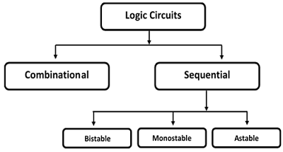
Sequential circuits are of three types −
Bistable − Bistable circuits have two stable operating points and will be in either of the states. Example − Memory cells, latches, flip-flops and registers.
Monostable − Monostable circuits have only one stable operating point and even if they are temporarily perturbed to the opposite state, they will return in time to their stable operating point. Example: Timers, pulse generators.
Astable − circuits have no stable operating point and oscillate between several states. Example − Ring oscillator.
CMOS Logic Circuits
SR Latch based on NOR Gate
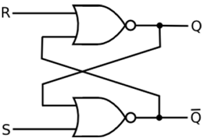
If the set input (S) is equal to logic "1" and the reset input is equal to logic "0." then the output Q will be forced to logic "1". While $\overline{Q}$ is forced to logic "0". This means the SR latch will be set, irrespective of its previous state.
Similarly, if S is equal to "0" and R is equal to "1" then the output Q will be forced to "0" while $\overline{Q}$ is forced to "1". This means the latch is reset, regardless of its previously held state. Finally, if both of the inputs S and R are equal to logic "1" then both output will be forced to logic "0" which conflicts with the complementarity of Q and $\overline{Q}$.
Therefore, this input combination is not allowed during normal operation. Truth table of NOR based SR Latch is given in table.
| S | R | Q | $\overline{Q}$ | Operation |
|---|---|---|---|---|
| 0 | 0 | Q | $\overline{Q}$ | Hold |
| 1 | 0 | 1 | 0 | Set |
| 0 | 1 | 0 | 1 | Reset |
| 1 | 1 | 0 | 0 | Not allowed |
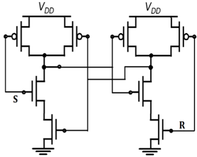
CMOS SR latch based on NOR gate is shown in the figure given below.
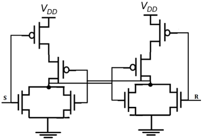
If the S is equal to VOH and the R is equal to VOL, both of the parallel-connected transistors M1 and M2 will be ON. The voltage on node $\overline{Q}$ will assume a logic-low level of VOL = 0.
At the same time, both M3 and M4 are turned off, which results in a logic-high voltage VOH at node Q. If the R is equal to VOH and the S is equal to VOL, M1 and M2 turned off and M3 and M4 turned on.
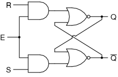
SR Latch based on NAND Gate
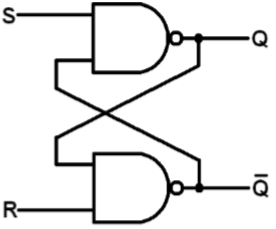
Block diagram and gate level schematic of NAND based SR latch is shown in the figure. The small circles at the S and R input terminals represents that the circuit responds to active low input signals. The truth table of NAND based SR latch is given in table
| S | R | Q | Q′ | |
| 0 | 0 | NC | NC | No change. Latch remained in present state. |
| 1 | 0 | 1 | 0 | Latch SET. |
| 0 | 1 | 0 | 1 | Latch RESET. |
| 1 | 1 | 0 | 0 | Invalid condition. |
If S goes to 0 (while R = 1), Q goes high, pulling $\overline{Q}$ low and the latch enters Set state
S = 0 then Q = 1 (if R = 1)
If R goes to 0 (while S = 1), Q goes high, pulling $\overline{Q}$ low and the latch is Reset
R = 0 then Q = 1 (if S = 1)
Hold state requires both S and R to be high. If S = R = 0 then output is not allowed, as it would result in an indeterminate state. CMOS SR Latch based on NAND Gate is shown in figure.
Depletion-load nMOS SR Latch based on NAND Gate is shown in figure. The operation is similar to that of CMOS NAND SR latch. The CMOS circuit implementation has low static power dissipation and high noise margin.
CMOS Logic Circuits
Clocked SR Latch
The figure shows a NOR-based SR latch with a clock added. The latch is responsive to inputs S and R only when CLK is high.
When CLK is low, the latch retains its current state. Observe that Q changes state −
- When S goes high during positive CLK.
- On leading CLK edge after changes in S & R during CLK low time.
- A positive glitch in S while CLK is high
- When R goes high during positive CLK.
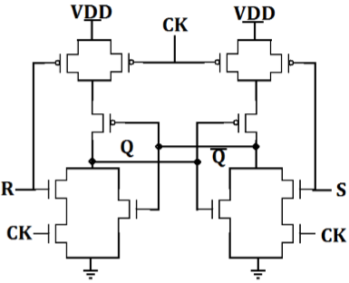
CMOS AOI implementation of clocked NOR based SR latch is shown in the figure. Note that only 12 transistors required.
When CLK is low, two series terminals in N tree N are open and two parallel transistors in tree P are ON, thus retaining state in the memory cell.
When clock is high, the circuit becomes simply a NOR based CMOS latch which will respond to input S and R.
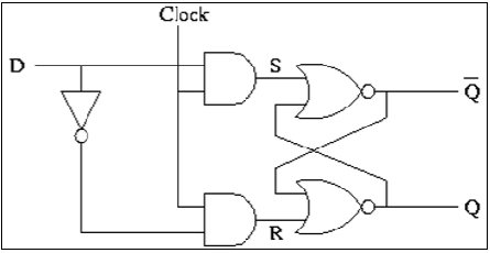
Clocked SR Latch based on NAND Gate
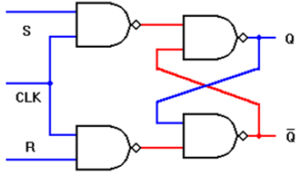
Circuit is implemented with four NAND gates. If this circuit is implemented with CMOS then it requires 16 transistors.
- The latch is responsive to S or R only if CLK is high.
- If both input signals and the CLK signals are active high: i.e., the latch output Q will be set when CLK = "1" S = "1" and R = "0"
- Similarly, the latch will be reset when CLK = "1," S = "0," and
When CLK is low, the latch retains its present state.
Clocked JK Latch
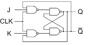
The figure above shows a clocked JK latch, based on NAND gates. The disadvantage of an SR latch is that when both S and R are high, its output state becomes indeterminant. The JK latch eliminates this problem by using feedback from output to input, such that all input states of the truth table are allowable. If J = K = 0, the latch will hold its present state.
If J = 1 and K = 0, the latch will set on the next positive-going clock edge, i.e. Q = 1, $\overline{Q}$ = 0
If J = 0 and K = 1, the latch will reset on the next positive-going clock edge, i.e. Q = 1 and $\overline{Q}$ = 0.
If J = K = 1, the latch will toggle on the next positive-going clock edge
The operation of the clocked JK latch is summarized in the truth table given in table.
J |
K |
Q |
$\overline{Q}$ | S |
R |
Q |
$\overline{Q}$ | Operation |
| 0 | 0 | 0 | 1 | 1 | 1 | 0 | 1 | Hold |
| 1 | 0 | 1 | 1 | 1 | 0 | |||
| 0 | 1 | 0 | 1 | 1 | 1 | 0 | 1 | Reset |
| 1 | 0 | 1 | 0 | 0 | 1 | |||
| 1 | 0 | 0 | 1 | 0 | 1 | 1 | 0 | Set |
| 1 | 0 | 1 | 1 | 1 | 0 | |||
| 1 | 1 | 0 | 1 | 0 | 1 | 1 | 0 | toggle |
| 1 | 0 | 1 | 0 | 0 | 1 |
CMOS D Latch Implementation
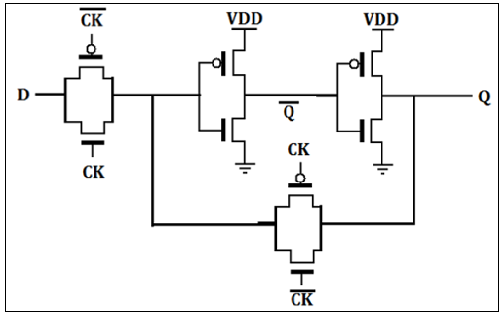
The D latch is normally, implemented with transmission gate (TG) switches as shown in the figure. The input TG is activated with CLK while the latch feedback loop TG is activated with CLK. Input D is accepted when CLK is high. When CLK goes low, the input is opencircuited and the latch is set with the prior data D.
