- VLSI Design - Home
- VLSI Design - Digital System
- VLSI Design - FPGA Technology
- VLSI Design - MOS Transistor
- VLSI Design - MOS Inverter
- Combinational MOS Logic Circuits
- Sequential MOS Logic Circuits
- VLSI Design Useful Resources
- VLSI Design - Quick Guide
- VLSI Design - Useful Resources
- VLSI Design - Discussion
VLSI Design - MOS Transistor
Complementary MOSFET (CMOS) technology is widely used today to form circuits in numerous and varied applications. Todays computers, CPUs and cell phones make use of CMOS due to several key advantages. CMOS offers low power dissipation, relatively high speed, high noise margins in both states, and will operate over a wide range of source and input voltages (provided the source voltage is fixed)
For the processes we will discuss, the type of transistor available is the Metal-Oxide-Semiconductor Field Effect Transistor (MOSFET). These transistors are formed as a sandwich consisting of a semiconductor layer, usually a slice, or wafer, from a single crystal of silicon; a layer of silicon dioxide (the oxide) and a layer of metal.
Structure of a MOSFET
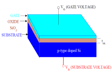
As shown in the figure, MOS structure contains three layers −
The Metal Gate Electrode
The Insulating Oxide Layer (SiO2)
P type Semiconductor (Substrate)
MOS structure forms a capacitor, with gate and substrate are as two plates and oxide layer as the dielectric material. The thickness of dielectric material (SiO2) is usually between 10 nm and 50 nm. Carrier concentration and distribution within the substrate can be manipulated by external voltage applied to gate and substrate terminal. Now, to understand the structure of MOS, first consider the basic electric properties of P Type semiconductor substrate.
Concentration of carrier in semiconductor material is always following the Mass Action Law. Mass Action Law is given by −
$$n.p=n_{i}^{2}$$
Where,
n is carrier concentration of electrons
p is carrier concentration of holes
ni is intrinsic carrier concentration of Silicon
Now assume that substrate is equally doped with acceptor (Boron) concentration NA. So, electron and hole concentration in ptype substrate is
$$n_{po}=\frac{n_{i}^{2}}{N_{A}}$$
$$p_{po}=N_{A}$$
Here, doping concentration NA is (1015 to 1016 cm−3) greater than intrinsic concentration ni. Now, to understand the MOS structure, consider the energy level diagram of ptype silicon substrate.
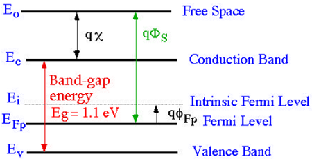
As shown in the figure, the band gap between conduction band and valance band is 1.1eV. Here, Fermi potential ΦF is the difference between intrinsic Fermi level (Ei) and Fermi level (EFP).
Where Fermi level EF depends on the doping concentration. Fermi potential ΦF is the difference between intrinsic Fermi level (Ei) and Fermi level (EFP).
Mathematically,
$$\Phi_{Fp}=\frac{E_{F}-E_{i}}{q}$$
The potential difference between conduction band and free space is called electron affinity and is denoted by qx.
So, energy required for an electron to move from Fermi level to free space is called work function (qΦS) and it is given by
$$q\Phi _{s}=(E_{c}-E_{F})+qx$$
The following figure shows the energy band diagram of components that make up the MOS.
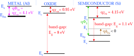
As shown in the above figure, insulating SiO2 layer has large energy band gap of 8eV and work function is 0.95 eV. Metal gate has work function of 4.1eV. Here, the work functions are different so it will create voltage drop across the MOS system. The figure given below shows the combined energy band diagram of MOS system.
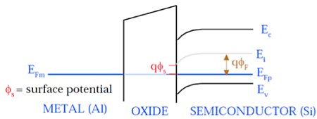
As shown in this figure, the fermi potential level of metal gate and semiconductor (Si) are at same potential. Fermi potential at surface is called surface potential ΦS and it is smaller than Fermi potential ΦF in magnitude.
Working of a MOSFET
MOSFET consists of a MOS capacitor with two p-n junctions placed closed to the channel region and this region is controlled by gate voltage. To make both the p-n junction reverse biased, substrate potential is kept lower than the other three terminals potential.
If the gate voltage will be increased beyond the threshold voltage (VGS>VTO), inversion layer will be established on the surface and n type channel will be formed between the source and drain. This n type channel will carry the drain current according to the VDS value.
For different value of VDS, MOSFET can be operated in different regions as explained below.
Linear Region
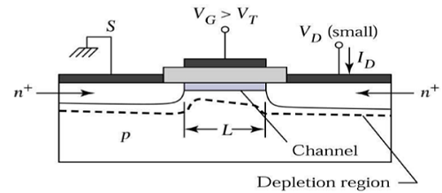
At VDS = 0, thermal equilibrium exists in the inverted channel region and drain current ID = 0. Now if small drain voltage, VDS > 0 is applied, a drain current proportional to the VDS will start to flow from source to drain through the channel.
The channel gives a continuous path for the flow of current from source to drain. This mode of operation is called linear region. The cross sectional view of an n-channel MOSFET, operating in linear region, is shown in the figure given below.
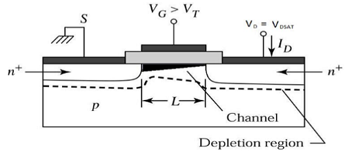
At the Edge of Saturation Region
Now if the VDS is increased, charges in the channel and channel depth decrease at the end of drain. For VDS = VDSAT, the charges in the channel is reduces to zero, which is called pinch off point. The cross sectional view of n-channel MOSFET operating at the edge of saturation region is shown in the figure given below.
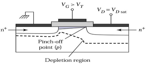
Saturation Region
For VDS>VDSAT, a depleted surface forms near to drain, and by increasing the drain voltage this depleted region extends to source.
This mode of operation is called Saturation region. The electrons coming from the source to the channel end, enter in the drain depletion region and are accelerated towards the drain in high electric field.
MOSFET Current Voltage Characteristics
To understand the current voltage characteristic of MOSFET, approximation for the channel is done. Without this approximation, the three dimension analysis of MOS system becomes complex. The Gradual Channel Approximation (GCA) for current voltage characteristic will reduce the analysis problem.
Gradual Channel Approximation (GCA)
Consider the cross sectional view of n channel MOSFET operating in the linear mode. Here, source and substrate are connected to the ground. VS = VB = 0. The gate to source (VGS) and drain to source voltage (VDS) voltage are the external parameters that control the drain current ID.
The voltage, VGS is set to a voltage greater than the threshold voltage VTO, to create a channel between the source and drain. As shown in the figure, x direction is perpendicular to the surface and y direction is parallel to the surface.
Here, y = 0 at the source end as shown in the figure. The channel voltage, with respect to the source, is represented by VC(Y). Assume that the threshold voltage VTO is constant along the channel region, between y = 0 to y = L. The boundary condition for the channel voltage VC are −
$$V_{c}\left ( y = 0 \right ) = V_{s} = 0 \,and\,V_{c}\left ( y = L \right ) = V_{DS}$$
We can also assume that
$$V_{GS}\geq V_{TO}$$ and
$$V_{GD} = V_{GS}-V_{DS}\geq V_{TO}$$
Let Q1(y) be the total mobile electron charge in the surface inversion layer. This electron charge can be expressed as −
$$Q1(y)=-C_{ox}.[V_{GS}-V_{C(Y)}-V_{TO}]$$
The figure given below shows the spatial geometry of the surface inversion layer and indicate its dimensions. The inversion layer taper off as we move from drain to source. Now, if we consider the small region dy of channel length L then incremental resistance dR offered by this region can be expressed as −
$$dR=-\frac{dy}{w.\mu _{n}.Q1(y)}$$
Here, minus sign is due to the negative polarity of the inversion layer charge Q1 and n is the surface mobility, which is constant. Now, substitute the value of Q1(y) in the dR equation −
$$dR=-\frac{dy}{w.\mu _{n}.\left \{ -C_{ox}\left [ V_{GS}-V_{C\left ( Y \right )} \right ]-V_{TO} \right \}}$$
$$dR=\frac{dy}{w.\mu _{n}.C_{ox}\left [ V_{GS}-V_{C\left ( Y \right )} \right ]-V_{TO}}$$
Now voltage drop in small dy region can be given by
$$dV_{c}=I_{D}.dR$$
Put the value of dR in the above equation
$$dV_{C}=I_{D}.\frac{dy}{w.\mu_{n}.C_{ox}\left [ V_{GS}-V_{C(Y)} \right ]-V_{TO}}$$
$$w.\mu _{n}.C_{ox}\left [ V_{GS}-V_{C(Y)}-V_{TO} \right ].dV_{C}=I_{D}.dy$$
To obtain the drain current ID over the whole channel region, the above equation can be integrated along the channel from y = 0 to y = L and voltages VC(y) = 0 to VC(y) = VDS,
$$C_{ox}.w.\mu _{n}.\int_{V_{c}=0}^{V_{DS}} \left [ V_{GS}-V_{C\left ( Y \right )}-V_{TO} \right ].dV_{C} = \int_{Y=0}^{L}I_{D}.dy$$
$$\frac{C_{ox}.w.\mu _{n}}{2}\left ( 2\left [ V_{GS}-V_{TO} \right ] V_{DS}-V_{DS}^{2}\right ) = I_{D}\left [ L-0 \right ]$$
$$I_{D} = \frac{C_{ox}.\mu _{n}}{2}.\frac{w}{L}\left ( 2\left [ V_{GS}-V_{TO} \right ]V_{DS}-V_{DS}^{2} \right )$$
For linear region VDS < VGS − VTO. For saturation region, value of VDS is larger than (VGS − VTO). Therefore, for saturation region VDS = (VGS − VTO).
$$I_{D} = C_{ox}.\mu _{n}.\frac{w}{2}\left ( \frac{\left [ 2V_{DS} \right ]V_{DS}-V_{DS}^{2}}{L} \right )$$
$$I_{D} = C_{ox}.\mu _{n}.\frac{w}{2}\left ( \frac{2V_{DS}^{2}-V_{DS}^{2}}{L} \right )$$
$$I_{D} = C_{ox}.\mu _{n}.\frac{w}{2}\left ( \frac{V_{DS}^{2}}{L} \right )$$
$$I_{D} = C_{ox}.\mu _{n}.\frac{w}{2}\left ( \frac{\left [ V_{GS}-V_{TO} \right ]^{2}}{L} \right )$$
