- VLSI Design - Home
- VLSI Design - Digital System
- VLSI Design - FPGA Technology
- VLSI Design - MOS Transistor
- VLSI Design - MOS Inverter
- Combinational MOS Logic Circuits
- Sequential MOS Logic Circuits
- VLSI Design Useful Resources
- VLSI Design - Quick Guide
- VLSI Design - Useful Resources
- VLSI Design - Discussion
Combinational MOS Logic Circuits
Combinational logic circuits or gates, which perform Boolean operations on multiple input variables and determine the outputs as Boolean functions of the inputs, are the basic building blocks of all digital systems. We will examine simple circuit configurations such as two-input NAND and NOR gates and then expand our analysis to more general cases of multiple-input circuit structures.
Next, the CMOS logic circuits will be presented in a similar fashion. We will stress the similarities and differences between the nMOS depletion-load logic and CMOS logic circuits and point out the advantages of CMOS gates with examples. In its most general form, a combinational logic circuit, or gate, performing a Boolean function can be represented as a multiple-input, single-output system, as depicted in the figure.
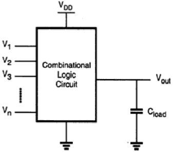
Node voltages, referenced to the ground potential, represent all input variables. Using positive logic convention, the Boolean (or logic) value of "1" can be represented by a high voltage of VDD, and the Boolean (or logic) value of "0" can be represented by a low voltage of 0. The output node is loaded with a capacitance CL, which represents the combined capacitances of the parasitic device in the circuit.
CMOS Logic Circuits
CMOS Two input NOR Gate
The circuit consists of a parallel-connected n-net and a series-connected complementary p-net. The input voltages VX and VY are applied to the gates of one nMOS and one pMOS transistor.
When either one or both inputs are high, i.e., when the n-net creates a conducting path between the output node and the ground, the p-net is cutoff. If both input voltages are low, i.e., the n-net is cut-off, then the p-net creates a conducting path between the output node and the supply voltage.
For any given input combination, the complementary circuit structure is such that the output is connected either to VDD or to ground via a low-resistance path and a DC current path between the VDD and ground is not established for any input combinations. The output voltage of the CMOS, two input NOR gate will get a logic-low voltage of VOL = 0 and a logic-high voltage of VOH = VDD. The equation of the switching threshold voltage Vth is given by
$$V_{th}\left ( NOR2 \right ) = \frac{V_{T,n}+\frac{1}{2}\sqrt{\frac{k_{p}}{k_{n}}\left ( V_{DD}-\left | V_{T,p} \right | \right )}}{1+\frac{1}{2}\sqrt{\frac{k_{p}}{k_{n}}}}$$
Layout of CMOS 2-input NOR Gate
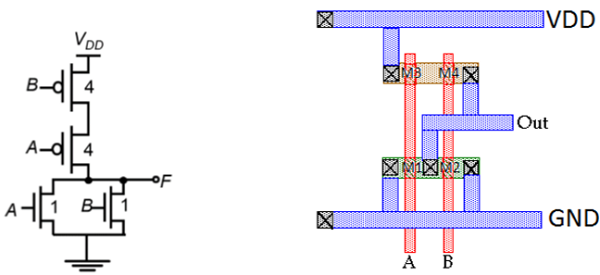
The figure shows a sample layout of CMOS 2-input NOR gate, using single-layer metal and single-layer polysilicon. The features of this layout are −
- Single vertical polylines for each input
- Single active shapes for N and P devices, respectively
- Metal buses running horizontal
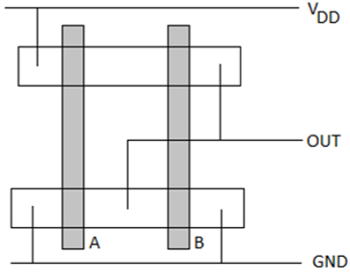
The stick diagram for the CMOS N0R2 gate is shown in the figure given below; which corresponds directly to the layout, but does not contain W and L information. The diffusion areas are depicted by rectangles, the metal connections and solid lines and circles, respectively represent contacts, and the crosshatched strips represent the polysilicon columns. Stick diagram is useful for planning optimum layout topology.
CMOS Two-input NAND Gate
The circuit diagram of the two input CMOS NAND gate is given in the figure below.
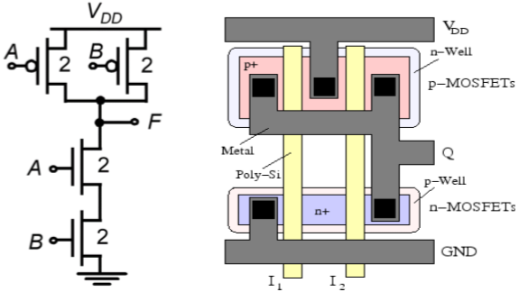
The principle of operation of the circuit is exact dual of the CMOS two input NOR operation. The n net consisting of two series connected nMOS transistor creates a conducting path between the output node and the ground, if both input voltages are logic high. Both of the parallelly connected pMOS transistor in p-net will be off.
For all other input combination, either one or both of the pMOS transistor will be turn ON, while p net is cut off, thus, creating a current path between the output node and the power supply voltage. The switching threshold for this gate is obtained as −
$$V_{th}\left ( NAND2 \right ) = \frac{V_{T,n}+2\sqrt{\frac{k_{p}}{k_{n}}\left ( V_{DD}-\left | V_{T,p} \right | \right )}}{1+2\sqrt{\frac{k_{p}}{k_{n}}}}$$
The features of this layout are as follows −
- Single polysilicon lines for inputs run vertically across both N and P active regions.
- Single active shapes are used for building both nMOS devices and both pMOS devices.
- Power bussing is running horizontal across top and bottom of layout.
- Output wires runs horizontal for easy connection to neighboring circuit.
Complex Logic Circuits
NMOS Depletion Load Complex Logic Gate
To realize complex functions of multiple input variables, the basic circuit structures and design principles developed for NOR and NAND can be extended to complex logic gates. The ability to realize complex logic functions, using a small number of transistors is one of the most attractive features of nMOS and CMOS logic circuits. Consider the following Boolean function as an example.
$$\overline{Z=P\left ( S+T \right )+QR}$$
The nMOS depletion-load complex logic gate used to realize this function is shown in figure. In this figure, the left nMOS driver branch of three driver transistors is used to perform the logic function P (S + T), while the right-hand side branch performs the function QR. By connecting the two branches in parallel, and by placing the load transistor between the output node and the supply voltage VDD, we obtain the given complex function. Each input variable is assigned to only one driver.
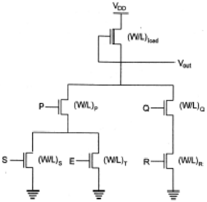
Inspection of the circuit topology gives simple design principles of the pull-down network −
- OR operations are performed by parallel-connected drivers.
- AND operations are performed by series-connected drivers.
- Inversion is provided by the nature of MOS circuit operation.
If all input variables are logic-high in the circuit realizing the function, the equivalent driver (W/L) ratio of the pull-down network consisting of five nMOS transistors is
$$\frac{W}{L}=\frac{1}{\frac{1}{\left ( W/L \right )Q}+\frac{1}{\left ( W/L \right )R}}+\frac{1}{\frac{1}{\left ( W/L \right )P}+\frac{1}{\left ( W/L \right )S+\left ( W/L \right )Q}}$$
Complex CMOS Logic Gates
The realization of the n-net, or pull-down network, is based on the same basic design principles examined for nMOS depletion-load complex logic gate. The pMOS pull-up network must be the dual network of the n-net.
It means all parallel connections in the nMOS network will correspond to a series connection in the pMOS network, and all series connection in the nMOS network correspond to a parallel connection in the pMOS network. The figure shows a simple construction of the dual p-net (pull-up) graph from the n-net (pull-down) graph.
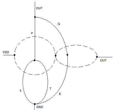
Each driver transistor in the pull-down network is shown by ai and each node is shown by a vertex in the pull-down graph. Next, a new vertex is created within each confined area in the pull graph, and neighboring vertices are connected by edges which cross each edge in the pull-down graph only once. This new graph shows the pull-up network.
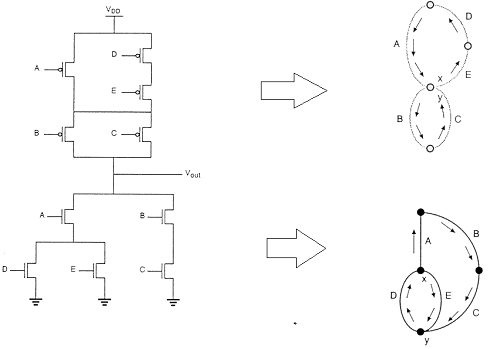
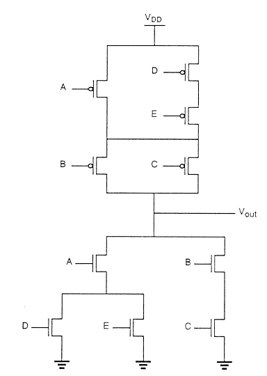
Layout Technique using Euler Graph Method
The figure shows the CMOS implementation of a complex function and its stick diagram done with arbitrary gate ordering that gives a very non-optimum layout for the CMOS gate.
In this case, the separation between the polysilicon columns must allow diffusion-todiffusion separation in between. This certainly consumes a considerably amount of extra silicon area.
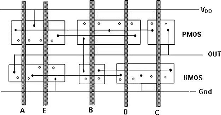
By using the Euler path, we can obtain an optimum layout. The Euler path is defined as an uninterrupted path that traverses each edge (branch) of the graph exactly once. Find Euler path in both the pull-down tree graph and the pull-up tree graph with identical ordering of the inputs.