- Microprocessor - Home
- Microprocessor Overview
- Microprocessor Classification
- Microprocessor Evolution
- Microprocessor Components
- Microprocessor Characteristics
- Microprocessor Functions
- Microprocessor Pros & Cons
- Microprocessor Application
- Microcontrollers Types
- Microcontrollers Pros & Cons
- 8085 Microprocessor Architecture
- 8085 Microprocessor Pin Configuration
- Addressing Modes & Interrupts
- 8085 Microprocessor Instruction Sets
- 8085 Microprocessor Features
- Externally Initiated Operations
- 8086 Microprocessor
- 8086 Microprocessor Overview
- Functional Units
- Pin Configuration
- Instruction Sets
- 8086 Microprocessor Interrupts
- 8086 Microprocessor Addressing Modes
- 8086 Microprocessor Features
- Memory Segmentation
- Auxiliary Carry Flag
- Maximum and Minimum Mode Configurations
- Multiprocessor Configuration
- Configuration Overview
- 8087 Numeric Data Processor
- I/O Interfacing
- I/O Interfacing Overview
- 8279 Programmable Keyboard
- 8257 DMA Controller
- Serial vs Parallel Communication
- Serial Communications Interface
- Parallel Communication Interface
- 8051 Microcontrollers
- Microcontrollers Overview
- 8051 Microcontrollers Architecture
- 8051 Pin Description
- 8051 Input Output Ports
- 8051 Microcontrollers Interrupts
- Instruction Sets
- Logical Instructions in AVR
- Conditional Branch Instructions AVR
- Arithmetic Instructions in AVR
- External Memory Interfacing
- Time Delay in AVR
- 8051 vs PIC Microcontroller
- Peripheral Devices
- Peripheral Devices
- Programmable Peripheral Interface
- Intel 8255A Pin Description
- Programmable Interval Timer
- 8253/54 Operational Modes
- Interfacing Devices
- Applications and Furture Trends
- Microcontrollers - Application
- Microprocessors and Microcontrollers in IoT
- Microcontrollers in Automotive Systems
- Microcontrollers - Low-Power
- Artificial Intelligence Processors
- Microprocessor Useful Resources
- Microprocessor - Quick Guide
- Microprocessor - Useful Resources
- Microprocessor - Discussion
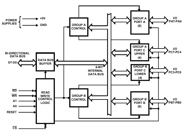
8255A - Programmable Peripheral Interface
The 8255A is a general purpose programmable I/O device designed to transfer the data from I/O to interrupt I/O under certain conditions as required. It can be used with almost any microprocessor.
It consists of three 8-bit bidirectional I/O ports (24I/O lines) which can be configured as per the requirement.
Ports of 8255A
8255A has three ports, i.e., PORT A, PORT B, and PORT C.
Port A contains one 8-bit output latch/buffer and one 8-bit input buffer.
Port B is similar to PORT A.
Port C can be split into two parts, i.e. PORT C lower (PC0-PC3) and PORT C upper (PC7-PC4) by the control word.
These three ports are further divided into two groups, i.e. Group A includes PORT A and upper PORT C. Group B includes PORT B and lower PORT C. These two groups can be programmed in three different modes, i.e. the first mode is named as mode 0, the second mode is named as Mode 1 and the third mode is named as Mode 2.
Operating Modes
8255A has three different operating modes −
Mode 0 − In this mode, Port A and B is used as two 8-bit ports and Port C as two 4-bit ports. Each port can be programmed in either input mode or output mode where outputs are latched and inputs are not latched. Ports do not have interrupt capability.
Mode 1 − In this mode, Port A and B is used as 8-bit I/O ports. They can be configured as either input or output ports. Each port uses three lines from port C as handshake signals. Inputs and outputs are latched.
Mode 2 − In this mode, Port A can be configured as the bidirectional port and Port B either in Mode 0 or Mode 1. Port A uses five signals from Port C as handshake signals for data transfer. The remaining three signals from Port C can be used either as simple I/O or as handshake for port B.
Features of 8255A
The prominent features of 8255A are as follows −
It consists of 3 8-bit IO ports i.e. PA, PB, and PC.
Address/data bus must be externally demux'd.
It is TTL compatible.
It has improved DC driving capability.
8255 Architecture
The following figure shows the architecture of 8255A −