
Article Categories
- All Categories
-
 Data Structure
-
 Networking
-
 RDBMS
RDBMS
-
 Operating System
-
 Java
Java
-
 MS Excel
-
 iOS
iOS
-
 HTML
HTML
-
 CSS
CSS
-
 Android
-
 Python
-
 C Programming
-
 C++
C++
-
 C#
C#
-
 MongoDB
-
 MySQL
MySQL
-
 Javascript
-
 PHP
PHP
-
 Economics & Finance
Unijunction Transistor – Construction, Working Principle, and Characteristic Features
A Unijunction Transistor (UJT) is a three-terminal semiconductor device. The main characteristics of UJT is when it is triggered, the emitter current increases re-generatively until it is limited by emitter power supply. Due to this characteristic feature, it is used in applications like switching pulse generator, saw-tooth wave generator etc.
Construction of UJT
The UJT consists of an n-type silicon semiconductor bar with an electrical on each end. The terminals of these connections are called Base terminals (B1 and B2). Near to base B2, a pn-junction is formed between a p-type emitter and the n-type silicon bar. The terminal of this junction is called emitter terminal (E).
Since the device has three terminals and one pn-junction, for this region this is called as a Unijunction Transistor (UJT).
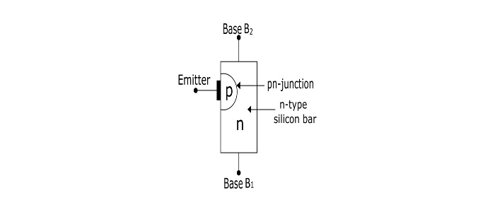

The device has only pn-junction so it forms a diode. Because the two base leads are taken from one section of the diode, hence the device is also called as Double-Based Diode.
The emitter is heavily doped while the n-region is lightly doped. Thus, the resistance between base terminals is very high when emitter terminal is open.
Operation of UJT
With Emitter Open
When the voltage VBB is applied with emitter open. A potential gradient is established along the n-type silicon bar. As the emitter is located close to the base B2, thus a major part of VBB appears between the emitter and base B1. The voltage V1 between emitter and B1, establishes a reverse bias on the pn-junction and the emitter current is cut off, but a small leakage current flows from B2 to emitter due to minority charge carriers. Thus, the device is said to be in OFF state.

With Emitter at Positive Potential
When a positive voltage is applied at the emitter terminal, the pn-junction will remain reverse biased till the input voltage is less than V1. A soon as the input voltage at emitter exceeds V1, the pn-junction becomes forward biased. Under this condition, holes are supplied from p-type region into the n-type bar. These holes are repelled by positive B2 terminal and attracted towards the B1 terminal. This increase in the number of holes in the emitter to B1 region results in the decrease of resistance of this section of the bar. Because of this, the internal voltage drop from emitter to B1 region is reduced, thus the emitter current (IE) increases. As more holes are supplied, a condition of saturation is reached. At the point of saturation, the emitter current is limited by the emitter power supply. Now, the device is conducting, hence said to be in ON state.

Equivalent Circuit of UJT
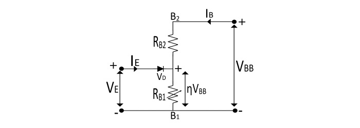
The resistance of silicon bar is called as the inter-base resistance (has a value from 4 kΩ to 10 kΩ).
The resistance RB1 is the resistance of the bar between emitter and B1 region. The value of this is variable and depends upon the bias voltage across the pn-junction.
The resistance RB2 is the resistance of the bar between emitter and B2 region.
The emitter pn-junction is represented by a diode.
With no voltage applied to the UJT, the value of inter-base resistance is given by
$$\mathrm{R_{BB}=R_{B1}+R_{B2}}$$
The intrinsic stand-off ration (?) of UJT is given by
$$\mathrm{\eta=\frac{V_{1}}{V_{BB}}=\frac{R_{B1}}{R_{B1}+R_{B2}}}$$
$$\mathrm{The\:voltage\:across\:R_{B1}\: is\:V_{1}=\frac{R_{B1}}{R_{B1}+R_{B2}}V_{BB}=\eta V_{BB}}$$
The value of ? generally lies between 0.51 and 0.82.
The Peak Point Voltage (VP) of the UJT
$$\mathrm{V_{p}=\eta V_{BB}+V_{D}}$$
Characteristics of UJT
The curve between emitter voltage (VE) and emitter current (IE) of UJT, at a given value of VBB is known as emitter characteristics of UJT.
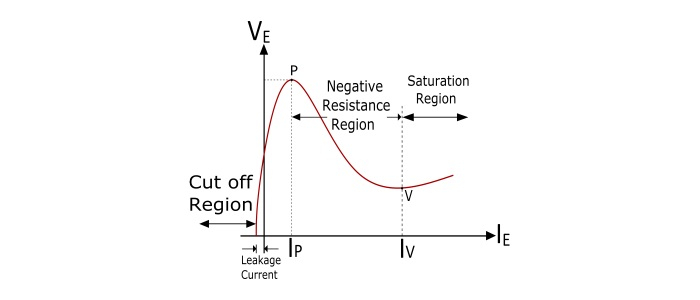
Important points from the characteristics are −
At first, in the cut off region, when the emitter voltage increases from zero, due to the minority charge carriers, a small current flows from terminal B2 to emitter. This is called as leakage current.
Above the definite value of VE, the emitter current (IE) starts to flow and increases until the peak (VP and IP) is reached at point P.
After point P, an increase in VE causes a sudden increase in IE with a corresponding decrease in VE. This is the Negative Resistance Region of the curve as with the increase in IE, VE decreases.
The negative resistance region of the curve ends at the valley-point (V), having valley-point voltage VV and current IV. After the valley-point the device is driven to saturation.
Advantages of UJT
Low cost
Excellent characteristics
Low power absorbing device under normal operating conditions
Applications of UJT
- Oscillators
- Trigger Circuits
- Saw tooth generator
- Bi-stable networks
- Pulse and voltage sensing circuits
- UJT relaxation oscillators
- Over voltage detectors
Numerical Example
A UJT has 20 V between the bases. If the intrinsic stand-off ratio is 0.75, find the value of stand-off voltage and peak-point voltage. Take the forward voltage drop in the pn-junction is 0.7 V.
Solution
$$\mathrm{Standoff\:voltage=\eta V_{BB}=0.75×20=15 V}$$
$$\mathrm{Peak−point\:Voltage\:(V_{p})=\eta V_{BB}+V_{D}=15+0.7=15.7 V}$$

99K+ Views
