Article Categories
- All Categories
-
 Data Structure
-
 Networking
-
 RDBMS
RDBMS
-
 Operating System
-
 Java
Java
-
 MS Excel
-
 iOS
iOS
-
 HTML
HTML
-
 CSS
CSS
-
 Android
-
 Python
-
 C Programming
-
 C++
C++
-
 C#
C#
-
 MongoDB
-
 MySQL
MySQL
-
 Javascript
-
 PHP
PHP
-
 Economics & Finance
Transistor Amplifier – Working Principle and Applications
Transistor as an Amplifier
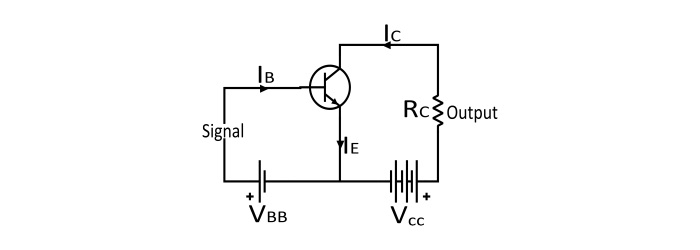
A transistor can increase the strength of a weak signal and hence it can be used as an amplifier in a circuit. The weak signal is applied between the emitter – base junction and output is taken across the load connected in the collector circuit.
In order to achieve desired amplification, emitter – base junction must remain forward biased. For this, a DC voltage VBB is applied in the input circuit in addition to signal. This DC voltage is known as Bias Voltage and its magnitude is such that it always makes the emitter – base junction forward biased regardless of polarity of signal.
Since the input circuit has low resistance (because of forward biased), hence a small change in signal voltage causes a huge change in emitter current. Due to transistor action, same change occurs in the collector current. Since the collector current flowing through a high load resistance RC produces a large voltage across it. In this way, a weak signal applied to the input circuit amplified in the output circuit, hence the transistor acts as an amplifier.
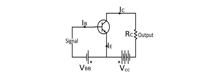
Circuit Diagram of Transistor Amplifier


Operation of Transistor Amplifier


During Positive half cycle of the input signal, the forward bias across emitter – base junction is increased. Hence, from the n – types emitter more electrons flow to the collector through the base. This increases the collector current. The increased collector current causes a high voltage drop across the collector load resistance (RC).
During the negative half cycle of the input signal, the forward bias across the emitter – base junction is decreased. Hence, the collector current decreased. This causes reduced output voltage in opposite direction. Therefore, amplified output is obtained across the load.
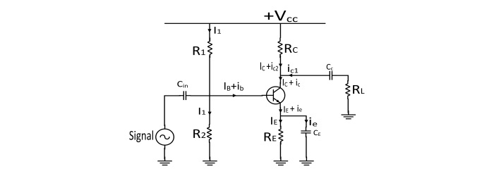
Practical Circuit of Transistor Amplifier

Description and function of various circuit elements of transistor amplifier −
Biasing and Stabilisation Circuit − The resistance R1, R2 and RE form the biasing and stabilisation circuit of the amplifier. The function of the biasing circuit is to establish a proper operating point otherwise some part of negative half cycle of input signal may be cut off in output.
Input Capacitor (Cin) − An electrolytic capacitor is used to couple the signal source to the transistor base. This capacitor allows only AC signal to flow and isolates the signal source from the resistance R2. If this capacitor is not used, then signal source resistance will come across R2 and change the bias.
Emitter Bypass Capacitor (CE) − This capacitor is used in parallel with RE to provide a path of low reactance to the amplified output AC signal. If this capacitor is not used, the amplified AC signal will flow through RE and cause a voltage drop across it and reduces the output voltage.
Coupling Capacitor (Cc) − The coupling capacitor couples one stage of amplification to the next stage. If this capacitor is not used, the RC will come in parallel with the resistance R1 of the next stage and alter the biasing network of next stage. Hence, coupling capacitor Cc isolates the DC of one stage from the next stage and allow the passes of AC signal only.
Performance of Transistor Amplifier
Input Resistance − Input resistance is defined as the ration of change in base – emitter voltage (ΔVBE) to the corresponding change in base current (ΔIB) at constant collector – emitter voltage.
The value of input resistance is very small since the input circuit is always forward biased.
$$\mathrm{input\:Resistance(R_{i})=\frac{ΔV_{BE}}{ΔI_{B}}}$$
Output Resistance − Output resistance of amplifier is defined as the change in collector – emitter voltage (ΔVGE) to the corresponding change in collector current (ΔIG) at constant base current.
The output resistance of a transistor amplifier is very large because the collector base junction is reverse biased.
$$\mathrm{Output\:Resistance\:(R_{0})=\frac{ΔV_{GE}}{ΔI_{G}}}$$
Effective Collector Load − Effective Collector Load is the total load as seen by the AC collector current.
$$\mathrm{Effective\:Collector\:Load (R_{eff.load})=R_{G}\:||\:R_{0}=\frac{R_{G}×R_{0}}{R_{G}+R_{0}}=\frac{R_{G}×R_{0}}{R_{0}}=R_{G}}$$
$$\mathrm{?\:R_{G}\:
Current Gain −Current gain is defined as the ratio of change in collector current (ΔIG) to the change in base current (ΔIB).
The value of β vary from 20 to 500.
$$\mathrm{Current\:Gain\:(β)=\frac{ΔI_{G}}{ΔI_{B}}}$$
Voltage Gain − It is defined as the ration of change in output voltage (ΔVGE) to the change in the input voltage (ΔVBE).
$$\mathrm{Voltage\:Gain\:(A_{\nu})=\frac{ΔV_{GE}}{ΔV_{BE}}=\frac{ΔI_{G}×R_{eff.load}}{ΔI_{B}×R_{i}}}$$
Power Gain − It is defined as the power of output signal to the power of input signal.
$$\mathrm{power\:Gain(A_{p})=\frac{(ΔI_{G})^2×R_{eff.load}}{(ΔI_{B})^2×R_{i}}=\frac{ΔI_{G}}{ΔI_{B}}×\frac{ΔI_{G}×R_{eff.load}}{ΔI_{B}×R_{i}}}$$
$$\mathrm{A_{p}=Current\:Gain ×Voltage\:Gain}$$
Numerical Example
For a transistor amplifier, the emitter current IE=9 mA, base input current IB=250 μA, Rc=4.5 kΩ,RE=2.5 kΩ. Determine (i) the current gain (ii) the voltage gain (iii) the power gain.
Solution
- The collector current
$$\mathrm{I_{C}=I_{E}-I_{B}=9 mA−250 μA=8.75 mA}$$
$$\mathrm{Current\:Gain(β)=\frac{I_{C}}{I_{B}}=\frac{8.75 mA}{250 μA}=35}$$
- Voltage Gain
$$\mathrm{A_{\nu}=\frac{ΔI_{C}×R_{off.load}}{ΔI_{B}×R_{i}}=\frac{R_{C}}{R_{E}}=\frac{4.5 kΩ}{2.5 kΩ}=1.8}$$
- Power Gain
$$\mathrm{A_{p}=A_{i}×A_{\nu}=35×1.8=63}$$


