
Article Categories
- All Categories
-
 Data Structure
-
 Networking
-
 RDBMS
RDBMS
-
 Operating System
-
 Java
Java
-
 MS Excel
-
 iOS
iOS
-
 HTML
HTML
-
 CSS
CSS
-
 Android
-
 Python
-
 C Programming
-
 C++
C++
-
 C#
C#
-
 MongoDB
-
 MySQL
MySQL
-
 Javascript
-
 PHP
PHP
-
 Economics & Finance
Physical Limitations of Operational Amplifiers
A practical operational amplifier exhibits some limitations that should be considered in the design of instrument.
The Physical Limitations of Operational Amplifier −
- Voltage Supply Limitations
- Finite Bandwidth Limitations
- Input Offset Voltage Limitations
- Input Bias Current Limitations
- Output Offset Voltage Limits
- Slew Rate Limitation
- Short Circuit Output Limits
- Limited Common Mode Rejection Ratio
Voltage Supply Limitations
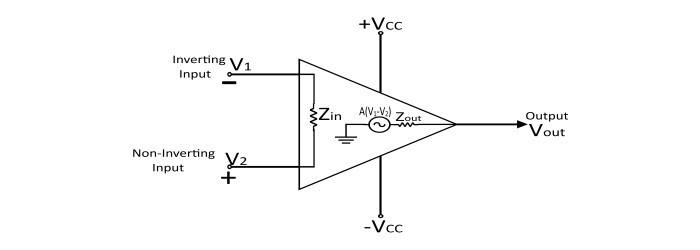
An operational amplifier is power by an external DC power supply (+VCC and -VCC), which are symmetric and of the order of ± 10 V to ± 20 V. The effect of voltage supply limits is that amplifiers are able to amplify the signals only within the range of their power supply voltage. It is physically impossible for an operational amplifier to generate voltage greater power supply voltage (VCC). For commercial operational amplifiers, the limit is approximately 1.5 V less than the VCC.
$$\mathrm{-V_{cc} The practical operational amplifier has finite bandwidth. The gain (A) of practical operational amplifier is the function of frequency and is characterised by a low-pass response. For an operational amplifier, $$\mathrm{A(j \omega)=\frac{A_{0}}{1+\frac{j \omega}{\omega_{0}}}}$$ The cut off frequency (ω0) of the Op-Amp represents the point where the amplifier response starts to decrease as a function of frequency. The finite bandwidth of a practical Op-Amp results in a constant gain-bandwidth product and the effect of this is that as the closed loop gain of Op-Amp is increased, its 3 dB bandwidth is reduced proportionally until, within the limit. When Op-Amp is used in the open loop mode, its gain would be equal to A0 and its 3 dB bandwidth would be equal to (ω0). Thus the constant gain-bandwidth product becomes A0ω0 = K. Now, if the amplifier is used in the closed loop mode, then its gain is much less than the open loop gain (A0) and the 3 dB bandwidth of the Op-Amp is increased proportionally. For a practical Op-Amp, in the absence of external inputs, there may be an input offset voltage present at the input of the Op-Amp. This input offset voltage is due to the mismatch in the internal circuit of the Op-Amp. The input offset voltage appears as the differential input voltage between the inverting and non-inverting input terminals. The presence of the input offset voltage will cause a DC bias error in the output of the amplifier. The input bias current is not exactly zero for a practical Op-Amp i.e. there is a small input bias current present at the inverting and non-inverting terminals of the Op-Amp. These currents are due to the internal construction of the input stages of the Op-Amp. The values of input bias currents depend on the semiconductor technology used in the construction of operational amplifiers. Due to the effect of input offset voltages and input offset currents there is another non-ideal characteristics of Op-Amp that is Output Offset Voltage. A practical Op-Amp can produce only a finite rate of change of the output voltage. This limit rate is called as the slew rate. There is a finite slew rate for a practical Op-Amp. $$\mathrm{S_{0}=(\frac{dV_{0}}{dt})_{max}}$$ In case of a practical Op-Amp, the internal source is not ideal since it cannot provide an infinite amount of load current. Hence, another non-ideal Op-Amp characteristic is that the maximum output current of the Op-Amp is limited by the short circuit output current (ISC). $$\mathrm{I_{out} For a practical Op-Amp, there is a limited common mode voltage range. For an Op-Amp the CMRR can be found in the data sheet of any particular Op-Amp. $$\mathrm{CMMR\:(in\:dB)=20\:log|\frac{A_{DM}}{A_{GM}}|}$$Finite Bandwidth Limitations
Input Offset Voltage
Input Bias Currents
Output Offset Voltage Limits
Slew Rate Limit
Short Circuit Output Current
Common Mode Rejection Ratio Limitation

3K+ Views
