
Article Categories
- All Categories
-
 Data Structure
-
 Networking
-
 RDBMS
RDBMS
-
 Operating System
-
 Java
Java
-
 MS Excel
-
 iOS
iOS
-
 HTML
HTML
-
 CSS
CSS
-
 Android
-
 Python
-
 C Programming
-
 C++
C++
-
 C#
C#
-
 MongoDB
-
 MySQL
MySQL
-
 Javascript
-
 PHP
PHP
-
 Economics & Finance
Explain the design and implementation of a simple microsequencer?
The microprogram sequence is a general-purpose building block for the microprogrammed control unit. The main objective of the microprogram sequencer is to demonstrate an address to the control memory so that microinstruction can be read and executed. The next address logic of the sequencer decides the particular address source to be loaded into the control address register. The figure shows the layout of the simple microsequencer.
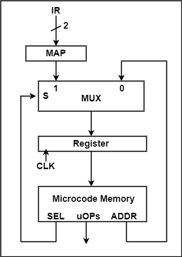
There are only two possible next addresses are used − the opcode mapping and an absolute jump. The last state of the fetch cycle, FETCH3, goes to one of the four execute routines. This must be implemented via the mapping input. The remaining state must each go to one specific next state, which we implement using an absolute jump. Although we could have implemented some of these branches by adding 1 to the current address, it cannot perform the branches from the end of each executes a routine to FETCH1 in this way.
The select bit is generated by the microsequencer to choose the correct next address. For this CPU, the selection is unconditional. In every state, this CPU knows with absolute certainty the source of its next address, but this is not the case for all microsequencers.
It contains a total of nine states, each of which is represented by one microinstruction. The minimum number of bits needed to select among them is 4, this is the size of the absolute address. The mapping hardware also generates an address of the same size, its output is also 4 bits wide. That is the same size as the output of the multiplexer that is input to the register and the output of the register that is input to the address inputs of the microcode memory.
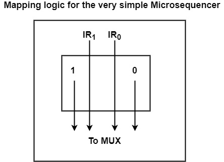
The primary consideration is the allocation of addresses for the first state of each execute routine since this determines the logic to implement the mapping function. For this CPU, the microsequencer will use the same mapping function that was used for the hardwired control unit, namely 1 IR [1…0]0.
This produces addresses of 1000, 1010, 1100, and 1110 (8, 10, 12, and 14) for ADD1, AND1, JMP1, and INC1, respectively. The hardware to implement the mapping becomes a few wires, which is the simplest possible mapping logic. This is shown in the figure.
The addresses for the remaining states can be assigned somewhat arbitrarily. It can assign consecutive states to consecutive locations in microcode memory. The resulting assignment is shown in the table.
State Address for the Very Simple Microsequencer
| State | Address |
|---|---|
| FETCH1 | 0000 (0) |
| FETCH2 | 0001 (1) |
| FETCH3 | 0010 (2) |
| ADD1 | 1000 (8) |
| ADD2 | 1001 (9) |
| AND1 | 1010 (10) |
| AND2 | 1011 (11) |
| JMP1 | 1100 (12) |
| INC1 | 1110 (14) |

1K+ Views
