
Article Categories
- All Categories
-
 Data Structure
-
 Networking
-
 RDBMS
RDBMS
-
 Operating System
-
 Java
Java
-
 MS Excel
-
 iOS
iOS
-
 HTML
HTML
-
 CSS
CSS
-
 Android
-
 Python
-
 C Programming
-
 C++
C++
-
 C#
C#
-
 MongoDB
-
 MySQL
MySQL
-
 Javascript
-
 PHP
PHP
-
 Economics & Finance
Enhancement Mode MOSFET
The Enhancement Mode Metal Oxide Semiconductor Field Effect Transistor (EMOSFET) is a three-terminal Device viz. Source (S), Gate (G) and Drain (D). The EMOSFET is a voltage controlled device.
The EMOSFET can be operated in the enhancement mode only. The EMOSFET has no physical channel from source to drain since the substrate extends completely to the SiO2 layer.
By the application of gate–source voltage (VGS) of proper magnitude and polarity the device can be made operating. The use of VGS induces an n-channel just below the gate terminal and this made the device operating.
The minimum value of VGS of proper polarity that turns on the EMOSFET is known as Threshold Voltage (VGS (Th)).
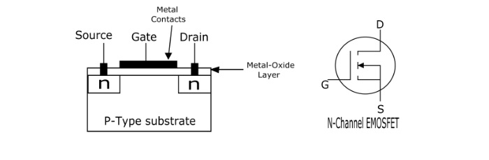
For the n−channel EMOSFET : +$\mathrm{V_{GS}\geqslant{V_{GS}}_{th}}$
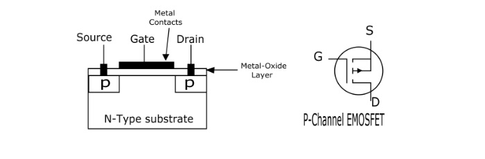
For the p−channel EMOSFET : −$\mathrm{V_{GS}\geqslant{V_{GS}}_{th}}$
Types of EMOSFET
- N-channel Enhancement MOSFET
- P-channel Enhancement MOSFET
Schematic Symbol of P-channel EMOSFET
Schematic Symbol of N-channel EMOSFET
Operation of EMOSFET
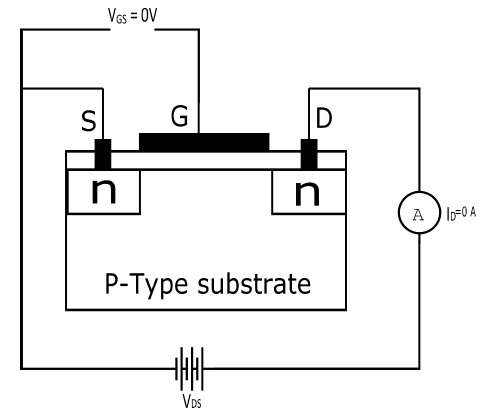
When VGS = 0 V, there is no channel connecting the source and drain. The p-type substrate has only a small number of thermally produced free electrons (minority charge carriers) so the drain current is zero. For this reason, the EMOSFET is generally OFF.
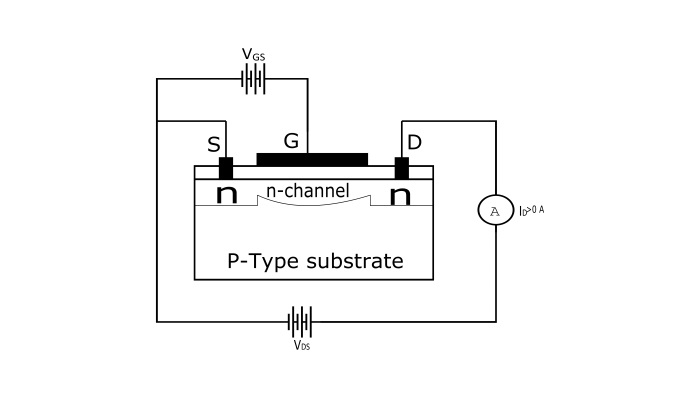
Now, when the gate is made positive, it attracts free electrons from p–substrate. The free electrons combine with the holes just below the SiO2 layer. If VGS is positive enough, all the holes touching the SiO2 layer are filled and remaining free electrons start flowing from source to drain. This is same as creating a thin layer of n–type material below the SiO2 layer, i.e., there is an induced n-channel through which the electrons flow takes place. Hence the EMOSFET is turned ON and drain current starts flowing from source to drain.
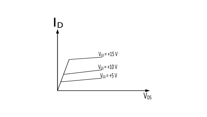
Drain Characteristics of EMOSFET
The drain characteristics is the graph between drain current and drain–source voltages for the various positive values of VGS. From the graph, it can be seen that most of the part of the curve is horizontal, showing constant drain current. Hence in this part of curve the EMOSFET behaves as a constant current source.
Transfer Characteristics of EMOSFET
The transfer characteristics of EMOSFET is the curve plotted between the drain current (ID) and gate-source voltage (VGS).
![]()
From this curve, it can be seen that, when VGS is less than VGS(th), there is no induced channel and the drain current (ID) is zero. When VGS is made equal to VGS(th), the EMOSFET is turned ON and the induced channel conducts from source to drain. The further increase in the value of VGS beyond VGSth increases the width of induced channel and hence, the drain current.
Transconductance Equation of EMOSFET
The equation for transconductance of EMOSFET (for VGS > VGS(th)) is given by
$$\mathrm{I_{D}=K(V_{GS}- {V_{GS}}_{(th)})^2}$$
The constant K depends upon a particular EMOSFET and its value can be determined from the equation
$$\mathrm{K=\frac{I_{D(on)}}{(V_{GS(on)-V_{GS(th)}})^2}}$$
The values of ID(on) and VGS(on) can be obtained from the data sheet for an EMOSFET.

22K+ Views
