
Article Categories
- All Categories
-
 Data Structure
-
 Networking
-
 RDBMS
RDBMS
-
 Operating System
-
 Java
Java
-
 MS Excel
-
 iOS
iOS
-
 HTML
HTML
-
 CSS
CSS
-
 Android
-
 Python
-
 C Programming
-
 C++
C++
-
 C#
C#
-
 MongoDB
-
 MySQL
MySQL
-
 Javascript
-
 PHP
PHP
-
 Economics & Finance
Accumulator or Register A in 8085 Microprocessor
Register A is an 8-bit register used in 8085 to perform arithmetic, logical, I/O & LOAD/STORE operations. Register A is quite often called as an Accumulator. An accumulator is a register for short-term, intermediate storage of arithmetic and logic data in a computer's CPU (Central Processing Unit).In an arithmetic operation involving two operands, one operand has tobe in this register. And the result of the arithmetic operation will be stored or accumulated in this register. Similarly, in a logical operation involving two operands, one operand has to be in the accumulator. Also, some other operations, like complementing and decimal adjustment, can be performed only on the accumulator.
Let us now consider a program segment which involves the content of Accumulate only. In 8085 Instruction set, STA is a mnemonic that stands for STore Accumulator contents in memory. In this instruction, Accumulator 8-bit content will be stored in a memory location whose 16-bit address is indicated in the instruction as a16. This instruction uses absolute addressing for specifying the destination. This instruction occupies 3-Bytes of memory. First Byte is required for the opcode, and next successive 2-Bytes provide the 16-bit address divided into 8-bits each consecutively.
| Mnemonics, Operand |
Opcode (in HEX) |
Bytes |
|---|---|---|
| STA Address |
32 |
3 |
Let us consider STA 4050 Has an example instruction of this type. It is a 3-Byte instruction. The first Byte will contain the opcode hex value 32H. As in 8085 assembly language coding supports low order Byte of the address should be mentioned at first then the high order Byte of the address should be mentioned next. So next Byte in memory will hold 50H and after that 40H will be kept in the last third Byte. Let us suppose the initial content of Accumulator is ABH and initial content of memory location 4050H is CDH. So after execution, Accumulator content will remain as ABH and 4050H location’s content will become ABH replacing its previous content CDH. The content tracing of this instruction has been shown below –
| Before |
After |
|
|---|---|---|
|
(A) |
ABH |
ABH |
|
(4050H) |
CDH |
ABH |
| Address |
Hex Codes |
Mnemonic |
Comment |
|---|---|---|---|
| 2008 |
2A |
STA 4050H |
The content of the memory location 4050H ← A |
| 2009 |
50 |
|
Low-order Byte of the address |
| 200A |
40 |
|
High order Byte of the address |
The timing diagram of this instruction STA 4050H is as follows -
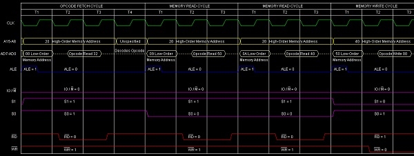
Summary − So this instruction SDA 4050H requires 3-Bytes, 4-Machine Cycles (Opcode Fetch, Memory Read, Memory Read, Memory Write) and 13 T-States for execution as shown in the timing diagram.

8K+ Views
