- Digital Electronics - Home
- Digital Electronics Basics
- Types of Digital Systems
- Types of Signals
- Logic Levels And Pulse Waveforms
- Digital System Components
- Digital Logic Operations
- Digital Systems Advantages
- Number Systems
- Number Systems
- Binary Numbers Representation
- Binary Arithmetic
- Signed Binary Arithmetic
- Octal Arithmetic
- Hexadecimal Arithmetic
- Complement Arithmetic
- Base Conversions
- Base Conversions
- Binary to Decimal Conversion
- Decimal to Binary Conversion
- Binary to Octal Conversion
- Octal to Binary Conversion
- Octal to Decimal Conversion
- Decimal to Octal Conversion
- Hexadecimal to Binary Conversion
- Binary to Hexadecimal Conversion
- Hexadecimal to Decimal Conversion
- Decimal to Hexadecimal Conversion
- Octal to Hexadecimal Conversion
- Hexadecimal to Octal Conversion
- Binary Codes
- Binary Codes
- 8421 BCD Code
- Excess-3 Code
- Gray Code
- ASCII Codes
- EBCDIC Code
- Code Conversion
- Error Detection & Correction Codes
- Logic Gates
- Logic Gates
- AND Gate
- OR Gate
- NOT Gate
- Universal Gates
- XOR Gate
- XNOR Gate
- CMOS Logic Gate
- OR Gate Using Diode Resistor Logic
- AND Gate vs OR Gate
- Two Level Logic Realization
- Threshold Logic
- Boolean Algebra
- Boolean Algebra
- Laws of Boolean Algebra
- Boolean Functions
- DeMorgan's Theorem
- SOP and POS Form
- POS to Standard POS Form
- Minimization Techniques
- K-Map Minimization
- Three Variable K-Map
- Four Variable K-Map
- Five Variable K-Map
- Six Variable K-Map
- Don't Care Condition
- Quine-McCluskey Method
- Min Terms and Max Terms
- Canonical and Standard Form
- Max Term Representation
- Simplification using Boolean Algebra
- Combinational Logic Circuits
- Digital Combinational Circuits
- Digital Arithmetic Circuits
- Multiplexers
- Multiplexer Design Procedure
- Mux Universal Gate
- 2-Variable Function Using 4:1 Mux
- 3-Variable Function Using 8:1 Mux
- Demultiplexers
- Mux vs Demux
- Parity Bit Generator and Checker
- Comparators
- Encoders
- Keyboard Encoders
- Priority Encoders
- Decoders
- Arithmetic Logic Unit
- 7-Segment LED Display
- Code Converters
- Code Converters
- Binary to Decimal Converter
- Decimal to BCD Converter
- BCD to Decimal Converter
- Binary to Gray Code Converter
- Gray Code to Binary Converter
- BCD to Excess-3 Converter
- Excess-3 to BCD Converter
- Adders
- Half Adders
- Full Adders
- Serial Adders
- Parallel Adders
- Full Adder using Half Adder
- Half Adder vs Full Adder
- Full Adder with NAND Gates
- Half Adder with NAND Gates
- Binary Adder-Subtractor
- Subtractors
- Half Subtractors
- Full Subtractors
- Parallel Subtractors
- Full Subtractor using 2 Half Subtractors
- Half Subtractor using NAND Gates
- Sequential Logic Circuits
- Digital Sequential Circuits
- Clock Signal and Triggering
- Latches
- Shift Registers
- Shift Register Applications
- Binary Registers
- Bidirectional Shift Register
- Counters
- Binary Counters
- Non-binary Counter
- Design of Synchronous Counter
- Synchronous vs Asynchronous Counter
- Finite State Machines
- Algorithmic State Machines
- Flip Flops
- Flip-Flops
- Conversion of Flip-Flops
- D Flip-Flops
- JK Flip-Flops
- T Flip-Flops
- SR Flip-Flops
- Clocked SR Flip-Flop
- Unclocked SR Flip-Flop
- Clocked JK Flip-Flop
- JK to T Flip-Flop
- SR to JK Flip-Flop
- Triggering Methods:Flip-Flop
- Edge-Triggered Flip-Flop
- Master-Slave JK Flip-Flop
- Race-around Condition
- A/D and D/A Converters
- Analog-to-Digital Converter
- Digital-to-Analog Converter
- DAC and ADC ICs
- Realization of Logic Gates
- NOT Gate from NAND Gate
- OR Gate from NAND Gate
- AND Gate from NAND Gate
- NOR Gate from NAND Gate
- XOR Gate from NAND Gate
- XNOR Gate from NAND Gate
- NOT Gate from NOR Gate
- OR Gate from NOR Gate
- AND Gate from NOR Gate
- NAND Gate from NOR Gate
- XOR Gate from NOR Gate
- XNOR Gate from NOR Gate
- NAND/NOR Gate using CMOS
- Full Subtractor using NAND Gate
- AND Gate Using 2:1 MUX
- OR Gate Using 2:1 MUX
- NOT Gate Using 2:1 MUX
- Memory Devices
- Memory Devices
- RAM and ROM
- Cache Memory Design
- Programmable Logic Devices
- Programmable Logic Devices
- Programmable Logic Array
- Programmable Array Logic
- Field Programmable Gate Arrays
- Digital Electronics Families
- Digital Electronics Families
- CPU Architecture
- CPU Architecture
OR Gate Using Diode Resistor Logic
A logic gate is a digital electronic circuit that is used to implement different kinds of logical and comparison operations. We have several types of logic gates such as OR Gate, AND Gate, NOT Gate, NAND Gate, NOR Gate, etc. Here, we will discuss the realization of OR Logic Gate using diode resistor logic, i.e. DL OR Gate. But before going into the realization of DL OR gate, let us discuss the basic of OR Gate.
What is OR Gate?
OR Gate is a logic circuit which may have two or more binary inputs and gives an output according to the combination of the inputs.
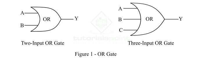
The OR Gate produces a logic 1 (HIGH) output, even if one of its input is in the logic 1 (HIGH) state. The OR Gate gives a logic 0 (LOW) output, only when each one of its inputs is in the logic 0 (LOW) state. Therefore, the OR gate is also referred to as any or all gate. It may also be called as an inclusive OR gate because it includes the state where both the inputs can be present. The symbols of a two input and a three input OR gate are shown in Figure-1.
OR Operation
The OR operation is represented by +. The Boolean expression for the output of OR gate is given below,
$$\mathrm{Y = A+B+C+ \cdot \cdot \cdot }$$
Where, Y is the output of the OR Gate, A, B, C are the input variables to the OR gate.
The operation of a logic gate is explained in terms of a truth table that represents the logical relationship between inputs and output.
Truth Table of OR Gate
The following table is the truth table of a three input OR Gate.
| Inputs | Output | ||
|---|---|---|---|
| A | B | C | Y = A + B + C |
| 0 | 0 | 0 | 0 |
| 0 | 0 | 1 | 1 |
| 0 | 1 | 0 | 1 |
| 0 | 1 | 1 | 1 |
| 1 | 0 | 0 | 1 |
| 1 | 0 | 1 | 1 |
| 1 | 1 | 0 | 1 |
| 1 | 1 | 1 | 1 |
OR Gate Using Diode Resistor Logic
We may realize the discrete OR gate by using diodes and resistors (called diode resistor logic). The circuit diagram of the OR Gate using diode resistor logic is shown in the following Figure-2.

Here, the inputs A and B to the gates may be either 0 V or +5 V. The operation of the OR Gate using diode-resistor logic is explained as follows
- When A = 0 V and B = 0 V, both the diodes D1 and D2 are off. Hence, there is no current flow through the resistor R, so there is no voltage drop across the resistor R. Consequently, the output voltage Y = 0 V.
- When A = +5 V and B = 0 V, then the diode D1 is on and the diode D2 is off. Thus, the output voltage Y = 5 V.
- When A = 0 V and B = +5 V, then the diode D1 is off and the diode D2 is on. Therefore, the output voltage Y = 5 V.
- When A = +5 V and B = +5 V, then both diodes D1 and D2 are on. Therefore, the output voltage Y = 5 V.
Note − In practice, there is a small voltage drop (about 0.7 V) takes place in diode itself. Hence, the output voltage Y = 5 0.7 = 4.3 V. This output voltage is regarded as logic 1.
Conclusion
From the above discussion, we can conclude that the OR Gate is a basic logic gate that is used to implement the operation of binary sum. The OR gate gives a logic 1 as output even if any of its inputs is at logic 1 state. It gives logic 0 output, only when all its inputs are at logic 0 state.
