
Article Categories
- All Categories
-
 Data Structure
-
 Networking
-
 RDBMS
RDBMS
-
 Operating System
-
 Java
Java
-
 MS Excel
-
 iOS
iOS
-
 HTML
HTML
-
 CSS
CSS
-
 Android
-
 Python
-
 C Programming
-
 C++
C++
-
 C#
C#
-
 MongoDB
-
 MySQL
MySQL
-
 Javascript
-
 PHP
PHP
-
 Economics & Finance
Electrical Analogue of Digital Logic Gates
Electrical analogue is basically a way of representing the operation of a logic gate such as OR gate, AND gate, NOT gate, etc. in the form of an electric circuit. In other words, we can represent the operation of a logic gate by using basic circuit components like battery, switches, lamps, etc. So, let us discuss the electrical analogue for each logic gate in detail.
OR Gate Electrical Circuit
The OR Gate is a type of logic circuit in digital electronics which may have two or more inputs but only one output. A two input OR gate is shown in Figure-1.

The output of the OR gate assumes the logic 1 state or HIGH, even if one of its inputs is in logic 1 state (HIGH). The output of the OR gate assumes the logic 0 state (LOW), only when each one of its inputs is in logic 0 state (LOW).
The operation of the two input OR gate can be analyzed with the help of its truth table given below.
| Inputs | Output | |
|---|---|---|
A |
B | Y = A + B |
| 0 | 0 | 0 |
| 0 | 1 | 1 |
| 1 | 0 | 1 |
| 1 | 1 | 1 |
With the help of this truth table, we can design an electrical circuit implementing the OR operation. The electrical circuit equivalent to OR operation is shown in Figure-2.
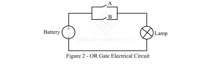
This electrical circuit representing two input OR gate operates as follows ?
When A = 0 (open) and B = 0 (open), the lamp will be OFF, i.e. output Y = 0.
When A = 0 (open) and B = 1 (close), the lamp will be ON, and current follows the path through switch B. Hence, the output Y = 1.
When A = 1 (close) and B = 0 (open), the lamp will be ON, i.e. current flow through switch A making the output Y = 1.
When A = 1 (close) and B = 1 (close), the lamp will be ON and current flows through both switches A and B. Thus, the output Y = 1.
Therefore, the electrical circuit shown in Figure-2 above is equivalent to OR gate.
AND Gate Electrical Circuit
The AND Gate is a type of logic circuit in digital electronics which may have two or more inputs but only one output. A two input AND gate is shown in Figure-3.

The output of the AND gate assumes the logic 0 state or LOW, even if one of its inputs is in logic 0 state (LOW). The output of the AND gate assumes the logic 1 state (HIGH), only when each one of its inputs is in logic 1 state (HIGH).
The operation of the two input AND gate can be analyzed with the help of its truth table given below.
| Inputs | Output | |
|---|---|---|
| A | B | Y = A B |
| 0 | 0 | 0 |
| 0 | 1 | 0 |
| 1 | 0 | 0 |
| 1 | 1 | 1 |
With the help of this truth table, we can design an electrical circuit implementing the AND operation. The electrical circuit equivalent to AND gate is shown in Figure-4.
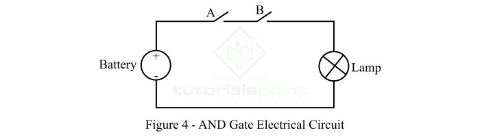
This electrical circuit representing two input AND gate operates as follows ?
When A = 0 (open) and B = 0 (open), the lamp will be OFF, no current can flow through the circuit. Hence, the output Y = 0.
When A = 0 (open) and B = 1 (close), the lamp will be OFF, because no current can flow through the circuit due to an open at switch A. Hence, the output Y = 0.
When A = 1 (close) and B = 0 (open), the lamp will be OFF, and no current flows through the circuit due to an open at switch B. Thus, the output Y = 0.
When A = 1 (close) and B = 1 (close), the lamp will be ON as there is no beak in the circuit, so current can flow. Thus, the output Y = 1.
Therefore, the electrical circuit shown in Figure-4 is equivalent to a two input AND gate.
NOT Gate Electrical Circuit
The NOT Gate is a type of logic circuit in digital electronics which have only one input and one output. The logic symbol of the NOT gate is shown in Figure-5.

The output of the NOT gate assumes the logic 0 state or LOW, when its input is in logic 1 state (HIGH). The output of the NOT gate assumes the logic 1 state (HIGH), when its input is in logic 0 state (LOW).
The operation of the two input NOT gate can be analyzed with the help of its truth table given below.
| Inputs | Output |
|---|---|
| A | Y = A? |
| 0 | 1 |
| 1 | 0 |
With the help of this truth table, we can design an electrical circuit implementing the NOT gate operation. The electrical circuit equivalent to the NOT gate is shown in Figure-6.
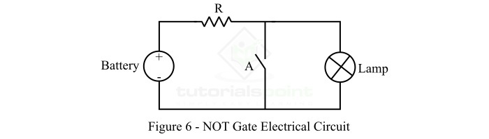
This electrical circuit representing the NOT gate operates as follows ?
When A = 0 (open), the current flows through the lamp making it ON. Hence, the output Y = 1.
When A = 1 (close), the current will bypass through the switch A making the lamp OFF. Hence, the output Y = 0.
Hence, the electric circuit shown in Figure-6 represents the NOT gate operation.
NAND Gate Electrical Circuit
The NAND Gate is a type of universal logic gate which may have two or more inputs but only one output. A two input NAND gate is shown in Figure-7.

The output of the NAND gate assumes the logic 1 state or HIGH, even if one of its inputs is in logic 0 state (LOW). The output of the NAND gate assumes the logic 0 state (LOW), only when each one of its inputs is in logic 1 state (HIGH).
The operation of the two input NOT gate can be analyzed with the help of its truth table given below.
| Inputs | Output | |
|---|---|---|
| A | B | Y = (AB)? |
| 0 | 0 | 1 |
| 0 | 1 | 1 |
| 1 | 0 | 1 |
| 1 | 1 | 0 |
With the help of this truth table, we can design an electrical circuit implementing the NAND operation. The electrical circuit equivalent to a two input NAND gate is shown in Figure-8.
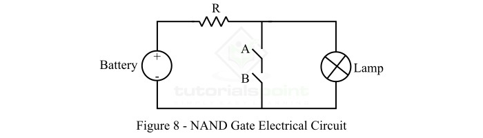
This electrical circuit representing the two input NAND gate operates as follows ?
When A = 0 (open) and B = 0 (open), the current will pass through the lamp making it ON. Hence, the output Y = 1.
When A = 0 (open) and B = 1 (close), the current will pass through the lamp making it ON. Hence, the output Y = 1.
When A = 1 (close) and B = 0 (open), the current will pass through the lamp making it ON. Thus, the output Y = 1.
When A = 1 (close) and B = 1 (close), the current will follow the short-circuited path provided by closed switches A and B, and no current will flow through the lamp making it OFF. Therefore, the output Y = 0.
Hence, the circuit shown in Figure-8 is electrical analogue to a two input NAND gate.
NOR Gate Electrical Circuit
The NOR Gate is another type of universal logic gate which may have two or more inputs but only one output. A two input NOR gate is shown in Figure-9.

The output of the NOR gate assumes the logic 0 state or LOW, even if one of its inputs is in logic 1 state (HIGH). The output of the NOR gate assumes the logic 1 state (HIGH), only when each one of its inputs is in logic 0 state (LOW).
The operation of the two input NOR gate can be analyzed with the help of its truth table given below.
| Inputs | Output | |
|---|---|---|
| A | B | Y = (A+B)? |
| 0 | 0 | 1 |
| 0 | 1 | 0 |
| 1 | 0 | 0 |
| 1 | 1 | 0 |
With the help of this truth table, we can design an electrical circuit implementing the NOR operation. The electrical circuit equivalent to a two input NOR gate is shown in Figure-10.
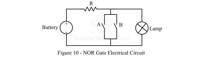
This electrical circuit representing the two input NOR gate operates as follows ?
When A = 0 (open) and B = 0 (open), the current will pass through the lamp making it ON. Hence, the output Y = 1.
When A = 0 (open) and B = 1 (close), the current will pass through short-circuited path provided by the switch B and no current will flow through the lamp making it OFF. Hence, the output Y = 0.
When A = 1 (close) and B = 0 (open), the current will pass through short-circuited path provided by the switch A, and no current will flow through the lamp making it OFF. Hence, the output Y = 0.
When A = 1 (close) and B = 1 (close), the current will pass through short-circuited paths provided by switches A & B, and no current will flow through the lamp making it OFF. Hence, the output Y = 0.
Hence, the circuit shown in Figure-10 is electrical analogue to a two input NOR gate.
Conclusion
This is all about electrical analogue of digital logic gates. From the above discussion, it is clear that all the logic gate operations like OR, AND, NOR, NAND, etc. can be represented with the help electrical circuits.

3K+ Views
