- CO - Home
- CO - Overview
- CO - Digital Number System
- CO - Number System Conversion
- CO - Binary Codes
- CO - Codes Conversion
- CO - Complement Arithmetic
- CO - Binary Arithmetic
- CO - Octal Arithmetic
- CO - Hexadecimal Arithmetic
- CO - Boolean Algebra
- CO - Logic Gates
- CO - Combinational Circuits
- CO - Sequential Circuits
- CO - Digital Registers
- CO - Digital Counters
- CO - Memory Devices
- CO - CPU Architecture
Quick Reference Guide
In the modern world of electronic, the term Digital is generally associated with a computer because the term Digital is derived from the way computers perform operation, by counting digits. For many year, the application of digital electronics was only in the computer system. But now-a-days, the digital electronic is used in many other application. Following are some of the examples in whihc Digital electronics is heavyily used.
Industrial process control
Military system
Television
Communication system
Medical equipment
Radar
navigation
Signal
Signal can be defined as a physical quantity, which contains some information. It is a function of one or more than one independent variables. Signal are of two types.
Analog Signal
Digital Signal
Analog Signal
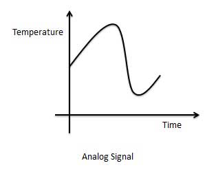
An analog signal is defined as the signal having continuous values. Analog signal can have infinite number of different values. In real world sceanario, most of the things observed in nature are analog. Examples of the analog signals are following.
Temperature
Pressure
Distance
Sound
Voltage
Current
Power
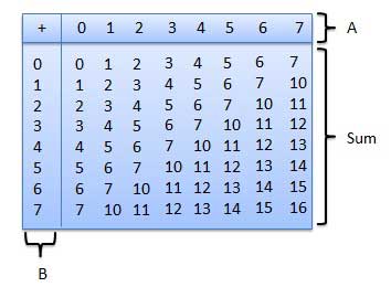
Graphical representation of Analog Signal (Temperature)
The circuits that process the analog signals are called as analog circuits or system. Examples of the analog system are following.
Filter
Amplifiers
Television receiver
motor speed controller
Disadvantage of the Analog Systems
Less accuracy
Less versatslity
More noise effect
More distortion
More effect of weather
Digital Signal
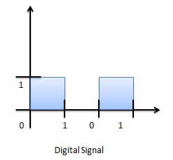
A digital signal is defined as the signal which has only a finite number of distinct values. Digital signal are not continuous signal. In the digital electronic calculator, the input is given with the help of switches. This input is converted into electrical signal which having two discrete values or levels. One of these may be called low level and another is called high level. The signal will always be one of the two levels. This type of signal is called digital signal. Examples of the digital signal are following.
Binary Signal
Octal Signal
Hexadecimal Signal
Graphical representation of the Digital Signal (Binary)
The circuit that process that digital signal are called digital system or digital circuit. Examples of the digital system are following.
Registers
Flip-flop
Counters
Microprocessors
Digital Number System
A digital system can understand positional number system only where there are only a few symbols called digits and these symbols represent different values depending on the position they occupy in the number.
A value of each digit in a number can be determined usingThe digit
The position of the digit in the number
The base of the number system (where base is defined as the total number of digits available in the number system).
Decimal Number System
The number system that we use in our day-to-day life is the decimal number system. Decimal number system has base 10 as it uses 10 digits from 0 to 9. In decimal number system, the successive positions to the left of the decimal point represent units, tens, hundreds, thousands and so on.
Each position represents a specific power of the base (10). For example, the decimal number 1234 consists of the digit 4 in the units position, 3 in the tens position, 2 in the hundreds position, and 1 in the thousands position, and its value can be written as
(1x1000)+ (2x100)+ (3x10)+ (4xl)
(1x10³)+ (2x10²)+ (3x101)+ (4xl00)
1000 + 200 + 30 + 1
1234
As a computer programmer or an IT professional, you should understand the following number systems which are frequently used in computers.
| S.N. | Number System & Description |
|---|---|
| 1 | Binary Number System Base 2. Digits used: 0, 1 |
| 2 | Octal Number System Base 8. Digits used: 0 to 7 |
| 4 | Hexa Decimal Number System Base 16. Digits used: 0 to 9, Letters used: A- F |
Binary Number System
Binary Number: 101012
Calculating Decimal Equivalent:
| Step | Binary Number | Decimal Number |
|---|---|---|
| Step 1 | 101012 | ((1 x 24) + (0 x 23) + (1 x 22) + (0 x 21) + (1 x 20))10 |
| Step 2 | 101012 | (16 + 0 + 4 + 0 + 1)10 |
| Step 3 | 101012 | 2110 |
Octal Number System
Octal Number: 125708
Calculating Decimal Equivalent:
| Step | Octal Number | Decimal Number |
|---|---|---|
| Step 1 | 125708 | ((1 x 84) + (2 x 83) + (5 x 82) + (7 x 81) + (0 x 80))10 |
| Step 2 | 125708 | (4096 + 1024 + 320 + 56 + 0)10 |
| Step 3 | 125708 | 549610 |
Hexadecimal Number System
Hexadecimal Number: 19FDE16
Calculating Decimal Equivalent:
| Step | Binary Number | Decimal Number |
|---|---|---|
| Step 1 | 19FDE16 | ((1 x 164) + (9 x 163) + (F x 162) + (D x 161) + (E x 160))10 |
| Step 2 | 19FDE16 | ((1 x 164) + (9 x 163) + (15 x 162) + (13 x 161) + (14 x 160))10 |
| Step 3 | 19FDE16 | (65536+ 36864 + 3840 + 208 + 14)10 |
| Step 4 | 19FDE16 | 10646210 |
Number System Conversion
There are many methods or techniques which can be used to convert numbers from one base to another. We'll demonstrate here the following
Decimal to Other Base System
Other Base System to Decimal
Other Base System to Non-Decimal
Shortcut method - Binary to Octal
Shortcut method - Octal to Binary
Shortcut method - Binary to Hexadecimal
Shortcut method - Hexadecimal to Binary
Base 10 to Base N Conversion
Steps
Step 1 - Divide the decimal number to be converted by the value of the new base.
Step 2 - Get the remainder from Step 1 as the rightmost digit (least significant digit) of new base number.
Step 3 - Divide the quotient of the previous divide by the new base.
Step 4 - Record the remainder from Step 3 as the next digit (to the left) of the new base number.
Repeat Steps 3 and 4, getting remainders from right to left, until the quotient becomes zero in Step 3.
The last remainder thus obtained will be the most significant digit (MSD) of the new base number.
Example
Decimal Number: 2910
Calculating Binary Equivalent:
| Step | Operation | Result | Remainder |
|---|---|---|---|
| Step 1 | 29 / 2 | 14 | 1 |
| Step 2 | 14 / 2 | 7 | 0 |
| Step 3 | 7 / 2 | 3 | 1 |
| Step 4 | 3 / 2 | 1 | 1 |
| Step 5 | 1 / 2 | 0 | 1 |
As mentioned in Steps 2 and 4, the remainders have to be arranged in the reverse order so that the first remainder becomes the least significant digit (LSD) and the last remainder becomes the most significant digit (MSD).
Decimal Number: 2910 = Binary Number: 111012.
Base N to Base 10 Conversion
Steps
Step 1 - Determine the column (positional) value of each digit (this depends on the position of the digit and the base of the number system).
Step 2 - Multiply the obtained column values (in Step 1) by the digits in the corresponding columns.
Step 3 - Sum the products calculated in Step 2. The total is the equivalent value in decimal.
Example
Binary Number: 111012
Calculating Decimal Equivalent:
| Step | Binary Number | Decimal Number |
|---|---|---|
| Step 1 | 111012 | ((1 x 24) + (1 x 23) + (1 x 22) + (0 x 21) + (1 x 20))10 |
| Step 2 | 111012 | (16 + 8 + 4 + 0 + 1)10 |
| Step 3 | 111012 | 2910 |
Binary Number: 111012 = Decimal Number: 2910
Base N to Base M Conversion
Steps
Step 1 - Convert the original number to a decimal number (base 10).
Step 2 - Convert the decimal number so obtained to the new base number.
Example
Octal Number: 258
Calculating Binary Equivalent:
Step 1: Convert to Decimal
| Step | Octal Number | Decimal Number |
|---|---|---|
| Step 1 | 278 | ((2 x 81) + (5 x 80))10 |
| Step 2 | 278 | (16 + 5 )10 |
| Step 3 | 278 | 2110 |
Octal Number: 258 = Decimal Number: 2110
Step 2: Convert Decimal to Binary
| Step | Operation | Result | Remainder |
|---|---|---|---|
| Step 1 | 21 / 2 | 10 | 1 |
| Step 2 | 10 / 2 | 5 | 0 |
| Step 3 | 5 / 2 | 2 | 1 |
| Step 4 | 2 / 2 | 1 | 0 |
| Step 5 | 1 / 2 | 0 | 1 |
Decimal Number: 2110 = Binary Number: 101012
Octal Number: 258 = Binary Number: 101012
Base 2 to Base 8 Conversion
Steps
Step 1 - Divide the binary digits into groups of three (starting from the right).
Step 2 - Convert each group of three binary digits to one octal digit.
Example
Binary Number: 101012
Calculating Octal Equivalent:
| Step | Binary Number | Octal Number |
|---|---|---|
| Step 1 | 101012 | 010 101 |
| Step 2 | 101012 | 28 58 38 |
| Step 3 | 101012 | 258 |
Binary Number: 101012 = Octal Number: 258
Base 8 to Base 2 Conversion
Steps
Step 1 - Convert each octal digit to a 3 digit binary number (the octal digits may be treated as decimal for this conversion).
Step 2 - Combine all the resulting binary groups (of 3 digits each) into a single binary number.
Example
Octal Number: 258
Calculating Binary Equivalent:
| Step | Octal Number | Binary Number |
|---|---|---|
| Step 1 | 258 | 210 510 |
| Step 2 | 258 | 0102 1012 |
| Step 3 | 258 | 0101012 |
Octal Number: 258 = Binary Number: 101012
Base 2 to Base 16 Conversion
Steps
Step 1 - Divide the binary digits into groups of four (starting from the right).
Step 2 - Convert each group of four binary digits to one hexadecimal symbol.
Example
Binary Number: 101012
Calculating hexadecimal Equivalent:
| Step | Binary Number | Hexadecimal Number |
|---|---|---|
| Step 1 | 101012 | 0001 0101 |
| Step 2 | 101012 | 110 510 |
| Step 3 | 101012 | 1516 |
Binary Number: 101012 = Hexadecimal Number: 1516
Base 16 to Base 2 Conversion
Steps
Step 1 - Convert each hexadecimal digit to a 4 digit binary number (the hexadecimal digits may be treated as decimal for this conversion).
Step 2 - Combine all the resulting binary groups (of 4 digits each) into a single binary number.
Example
Hexadecimal Number: F16
Calculating Binary Equivalent:
| Step | Hexadecimal Number | Binary Number |
|---|---|---|
| Step 1 | F16 | 1510 |
| Step 2 | F16 | 110 510 |
| Step 3 | F16 | 00012 01012 |
| Step 4 | F16 | 000101012 |
Hexadecimal Number: F16 = Binary Number: 101012
Binary Codes
In the coding, when numbers, letters or words are represented by a specific group of symbols, it is said that the number, letter or word is being encoded. The group of symbols is called as a code. The digital data is represented, stored and transmitted as group of binary bits. This group is also called as binary code. The binary code is represented by the number as well as alphanumeric letter.
Advantages of Binary Code
Following is the list of advantages that binary code offers.
Binary codes are suitable for the computer applications.
Binary codes are suitable for the digital communications.
Binary codes make the analysis and designing of digital circuits if we use the binary codes.
Since only 0 & 1 are being used, implementation becomes easy.
Classification of binary codes
The codes are broadly categorised into following four categories.
Weighted Codes
Non-Weighted Codes
Binary Coded Decimal Code
Alphanumeric Codes
Error Detecting Codes
Error Correcting Codes
Weighted Codes
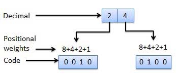
Weighted binary codes are those binary codes which obey the positional weight principle. Each position of the number represents a specific weight. Several system of the codes are used to express the decimal digits 0 through 9. In these codes each decimal digit is represented by a group of four bits.
Non-Weighted Codes
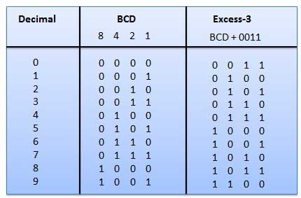
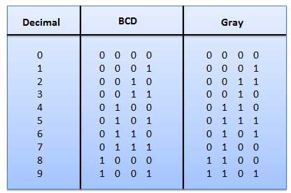
In this type of binary codes, the positional weights are not assigned. The example of non-weighted codes are Excess-3 code and Gray code.
Excess-3 code
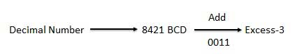
The Excess-3 code is also called as XS-3 code. It is non-weighted code used to express decimal numbers. The Excess-3 code words are derived from the 8421 BCD code words adding (0011)2 or (3)10 to each code word in 8421. The excess-3 codes are obtained as follows
Example
Gray Code
It is the another non-weighted code and it is not arithmetic codes. That means there are no specific weights assigned to the bit position. It has a very special feature that has only one bit will change, each time the decimal number is incremented as shown in fig.As only one bit changes at a time, the gray code is called as a unit distance code. The gray code is a cyclic code. Gray code can not be used for arithmetic operation.
Application of Gray code
Gray code is popularly used in the shaft position encoders.
A shaft position encoder produces a code word which represents the angular position of the shaft.
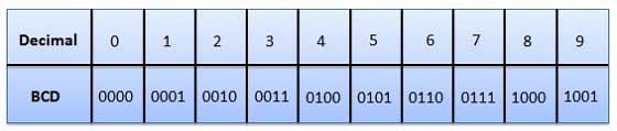
Binary Coded Decimal (BCD) code
In this code each decimal digit is represented by a 4-bit binary number. BCD is a way to express each of the decimal digits with a binary code. In the BCD, with four bits we can represent sixteen numbers (0000 to 1111). But in BCD code only first ten of these are used (0000 to 1001). The remaining six code combinations i.e. 1010 to 1111 are invalid in BCD.
Advantages of BCD Codes
It is very similar to decimal system.
We need to remember binary equivalent of decimal numbers 0 to 9 only.
Disadvantages of BCD Codes
The addition and subtraction of BCD have different rules.
The BCD arithmetic is little more complicated.
BCD need more number of bits than binary to represent the decimal number. So BCD is less efficient than binary.
Alphanumeric codes
A binary digit or bit can represent only two symbols as it has only two states '0' or '1'. But this is not enough for communication between two computers because there we need many more symbols for communication. These symbols are required to represent 26 alphabets with capital and small letters , numbers from 0 to 9 , punctuation marks and other symbols.
The alphanumeric codes are the codes that represent numbers and alphabetic characters. Mostly such codes also represent other characters such as symbol and various instruction necessary for conveying information. An alphanumeric code should at least represent 10 digits and 26 letters of alphabet i.e. total 36 items. The following three alphanumeric codes are very commonly used for the data representation.
American Standard Code for Information Interchange (ASCII).
Extended Binary Coded Decimal Interchange Code (EBCDIC).
Five bit Baudot Code.
ASCII code is a 7-bit code whereas EBCDIC is an 8-bit code. ASCII code is more commonly used world wide while EBCDIC is used primarily in large IBM computers.
Complement Arithmetic
Complements are used in the digital computers in order to simplify the subtraction operation and for the logical manipulations. For each radix-r system (radix r represent base of number system) there are two types of complements
| S.N. | Complement | Description |
|---|---|---|
| 1 | Radix Complement | The radix complement is referred to as the r's complement |
| 1 | Diminished Radix Complement | The diminished radix complement is referred to as the (r-1)'s complement |
Binary system complements
As the binary system has base r = 2. So the two types of complements for the binary system are 2's complement and 1's complement.
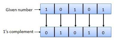
1's complement
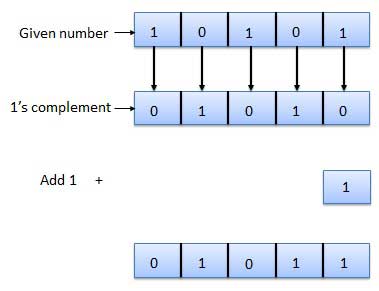
The 1's complement of a number is found by changing all 1's to 0's and all 0's to 1's. This is called as taking complement or 1's complement. Example of 1's Complement is as follows.
2's complement
The 2's complement of binary number is obtained by adding 1 to the Least Significant Bit (LSB) of 1's complement of the number.
2's complement = 1's complement + 1
Example of 2's Complement is as follows.
Binary Arithmetic
Binary arithmetic is essential part of all the digital computers and many other digital system.
Binary Addition
It is a key for binary subtraction, multiplication, division. There four rules of the binary addition.
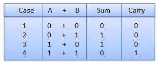
In fourth case, a binary addition is creating a sum of (1+1=10) i.e. 0 is write in the given column and a carry of 1 over to the next column.
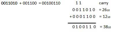
Example - Addition
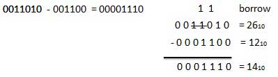
Binary Subtraction
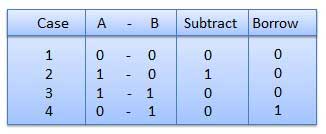
Subtraction and Borrow, these two words will be used very frequently for the binary subtraction.There four rules of the binary substration.There four rules of the binary substraction.
Example - Substraction
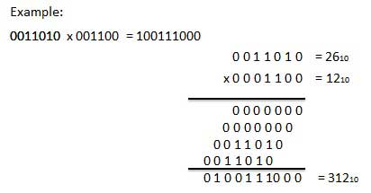
Binary Multiplication
Binary multiplication is similar to decimal multiplication. It is simpler than decimal multiplication because only 0s and 1s are involved.There four rules of the binary multiplication.
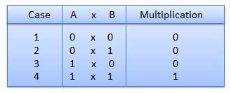
Example - Multiplication
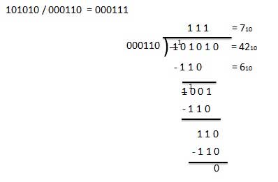
Binary Division
Binary division is similar to decimal division. It is called as the long division procedure.
Example - Division
Octal Arithmetic
Octal Number System
Following are the characteristics of an octal number system.
Uses eight digits, 0,1,2,3,4,5,6,7.
Also called base 8 number system
Each position in a octal number represents a 0 power of the base (8). Example 80
Last position in a octal number represents a x power of the base (8). Example 8x where x represents the last position - 1.
Example
Octal Number: 125708
Calculating Decimal Equivalent:
| Step | Octal Number | Decimal Number |
|---|---|---|
| Step 1 | 125708 | ((1 x 84) + (2 x 83) + (5 x 82) + (7 x 81) + (0 x 80))10 |
| Step 2 | 125708 | (4096 + 1024 + 320 + 56 + 0)10 |
| Step 3 | 125708 | 549610 |
Note: 125708 is normally written as 12570.
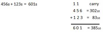
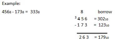
Octal Addition
Following octal addition table will help you greatly to handle Octal addition.
To use this table, simply follow the directions used in this example: Add: 68 and 58.Locate 6 in the A column then locate the 5 in the B column. The point in sum area where these two columns intersect is the sum of two number.
68 + 58 = 138.
Example - Addition
Octal Substraction
The subtraction of octal numbers follows the same rules as the subtraction of numbers in any other number system. The only variation is in borrowed number. In the decimal system, you borrow a group of 1010. In the binary system, you borrow a group of 210. In the octal system you borrow a group of 810.Example - Substraction
Hexadecimal Arithmetic
Hexadecimal Number System
Following are the characteristics of a hexadecimal number system.
Uses 10 digits and 6 letters, 0,1,2,3,4,5,6,7,8,9,A,B,C,D,E,F.
Letters represents numbers starting from 10. A = 10. B = 11, C = 12, D = 13, E = 14, F = 15.
Also called base 16 number system
Each position in a hexadecimal number represents a 0 power of the base (16). Example 160
Last position in a hexadecimal number represents a x power of the base (16). Example 16x where x represents the last position - 1.
Example
Hexadecimal Number: 19FDE16
Calculating Decimal Equivalent:
| Step | Binary Number | Decimal Number |
|---|---|---|
| Step 1 | 19FDE16 | ((1 x 164) + (9 x 163) + (F x 162) + (D x 161) + (E x 160))10 |
| Step 2 | 19FDE16 | ((1 x 164) + (9 x 163) + (15 x 162) + (13 x 161) + (14 x 160))10 |
| Step 3 | 19FDE16 | (65536+ 36864 + 3840 + 208 + 14)10 |
| Step 4 | 19FDE16 | 10646210 |
Note: 19FDE16 is normally written as 19FDE.
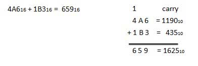
Hexadecimal Addition
Following hexadecimal addition table will help you greatly to handle Hexadecimal addition.
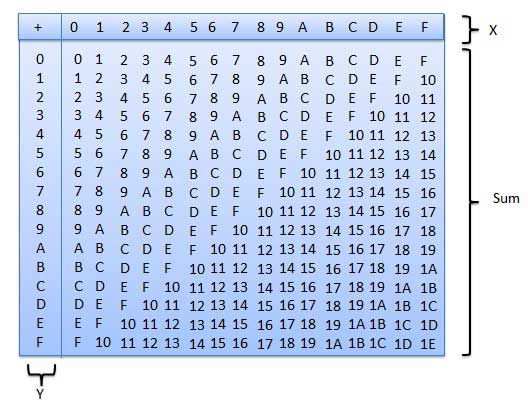
To use this table, simply follow the directions used in this example: Add: A16 and 516.Locate A in the X column then locate the 5 in the Y column. The point in sum area where these two columns intersect is the sum of two number.
A16 + 516 = F16.
Example - Addition
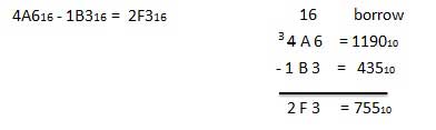
Hexadecimal Substraction
The subtraction of octal numbers follows the same rules as the subtraction of numbers in any other number system. The only variation is in borrowed number. In the decimal system, you borrow a group of 1010. In the binary system, you borrow a group of 210. In the hexadecimal system you borrow a group of 1610.Example - Substraction
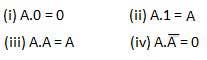
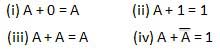
Boolean Algebra
Boolean Algebra is used to analyze and simplify the digital (logic) circuits. It uses only the binary numbers i.e. 0 and 1. It is also called as Binary Algebra or logical Algebra. Boolean algebra was invented by George Boole in 1854.
Rule in boolean algebra
Following are the important rules used in boolean algrebra.
Variable used can have only two values. Binary 1 for HIGH and Binary 0 for LOW.
Complement of a variable is represented by a overbar (-). Thus complement of variable B is represented as
 . Thus if B = 0 then = 1 and B = 1 then = 0.
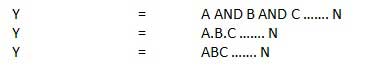
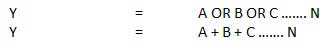
ORing of the variables is represented by a plus (+) sign between them. For example ORing of A, B, C is represented as A + B + C.
Logical ANDing of the two or more variable is represented by writing a dot between them such as A.B.C. Sometime the dot may be omitted like ABC.
Boolean Laws
There are six types of Boolean Laws.
Commutative law
Any binary operation which satisfies the following expression is referred to as commutative operation
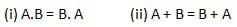
Commutative law states that changing the sequence of the variables does not have any effect on the output of a logic circuit.
Associative law
This law states that the order in which the logic operation are performed is irrelevant as their effect is the same.

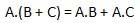
Distributive law
Distributive law states the following condition.
AND law
These laws use the AND operation. Therefore they are called as AND laws.
OR law
These laws use the OR operation. Therefore they are called as OR laws.
INVERSION law
This law uses the NOT operation. The inversion law states that double inversion of a variable result in the original variable itself.

Important Boolean Theroems
Following are few important boolean theroems.
| Boolean function/theroems | Description |
|---|---|
| Boolean Functions | Boolean Functions and Expressions, K-Map and NAND Gates realization |
| De Morgan's Theorems | De Morgan's Theorem 1 and Theorem 2 |
Logic Gates
Logic gates are the basic building blocks of any digital system. It is an electronic circuit having one or more than one input and only one output. The relationship between the input and the output is based on a certain logic. Based on this logic gates are named as AND gate, OR gate, NOT gate etc.
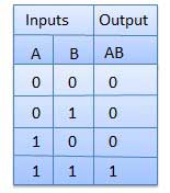
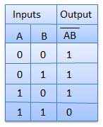
AND Gate
A circuit which performs an AND operation is shown in figure. It has n input (n >= 2) and one output.
Logic diagram
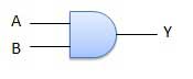
Truth Table
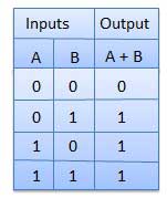
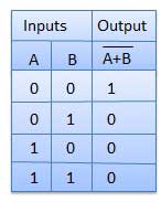
OR Gate
A circuit which performs an OR operation is shown in figure. It has n input (n >= 2) and one output.
Logic diagram
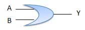
Truth Table
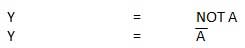
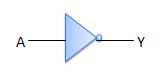
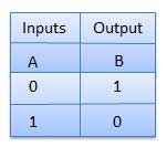
NOT Gate
NOT gate is also known as Inverter. It has one input A and one output Y.
Logic diagram
Truth Table
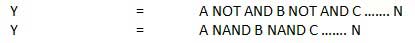
NAND Gate
A NOT-AND operation is known as NAND operation. It has n input (n >= 2) and one output.
Logic diagram
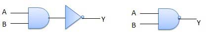
Truth Table
NOR Gate
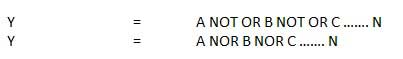
A NOT-OR operation is known as NOR operation. It has n input (n >= 2) and one output.
Logic diagram
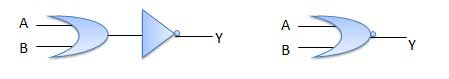
Truth Table
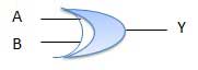
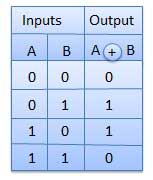
XOR Gate
XOR or Ex-OR gate is a special type of gate. It can be used in the half adder, full adder and subtractor. The exclusive-OR gate is abbreviated as EX-OR gate or sometime as X-OR gate. It has n input (n >= 2) and one output.
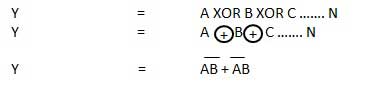
Logic diagram
Truth Table
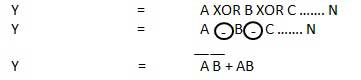
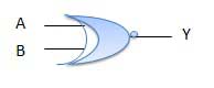
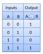
XNOR Gate
XNOR gate is a special type of gate. It can be used in the half adder, full adder and subtractor. The exclusive-NOR gate is abbreviated as EX-NOR gate or sometime as X-NOR gate. It has n input (n >= 2) and one output.
Logic diagram
Truth Table
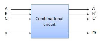
Combinational Circuits
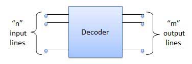
Combinational circuit is circuit in which we combine the different gates in the circuit for example encoder, decoder, multiplexer and demultiplexer. Some of the characteristics of combinational circuits are following.
The output of combinational circuit at any instant of time, depends only on the levels present at input terminals.
The combinational circuit do not use any memory. The previous state of input does not have any effect on the present state of the circuit.
A combinational circuit can have a n number of inputs and m number of outputs.
Block diagram
We're going to elaborate few important combinational circuits as follows.
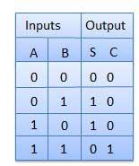
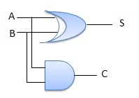
Half Adder
Half adder is a combinational logic circuit with two input and two output. The half adder circuit is designed to add two single bit binary number A and B. It is the basic building block for addition of two single bit numbers. This circuit has two outputs carry and sum.
Block diagram
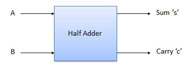
Truth Table
Circuit Diagram
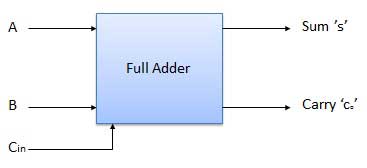
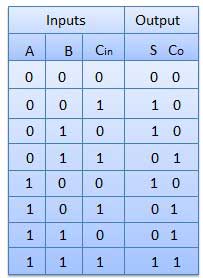
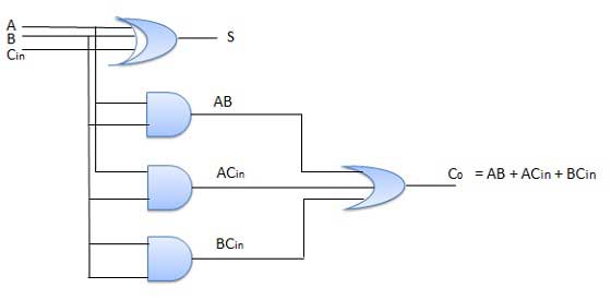
Full Adder
Full adder is developed to overcome the drawback of Half Adder circuit. It can add two one-bit numbers A and B, and carry c. The full adder is a three input and two output combinational circuit.
Block diagram
Truth Table
Circuit Diagram
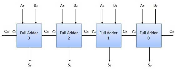
N-Bit Parallel Adder
The Full Adder is capable of adding only two single digit binary number along with a carry input. But in practical we need to add binary numbers which are much longer than just one bit. To add two n-bit binary numbers we need to use the n-bit parallel adder. It uses a number of full adders in cascade. The carry output of the previous full adder is connected to carry input of the next full adder.
4 Bit Parallel Adder
In the block diagram, A0 and B0 represent the LSB of the four bit words A and B. Hence Full Adder-0 is the lowest stage. Hence its Cin has been permanently made 0. The rest of the connection are exactly same as those of n-bit parallel adder is shown in fig. The four bit parallel adder is a very common logic circuit.
Block diagram
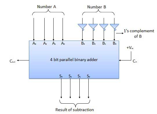
N-Bit Parallel Substractor
The subtraction can be carried out by taking the 1's or 2's complement of the number to be subtracted. For example we can perform the subtraction (A-B) by adding either 1's or 2's complement of B to A. That means we can use a binary adder to perform the binary subtraction.
4 Bit Parallel Subtractor
The number to be subtracted (B) is first passed through inverters to obtain its 1's complement. The 4-bit adder then adds A and 2's complement of B to produce the subtraction. S3 S2 S1 S0 represent the result of binary subtraction (A-B) and carry output Cout represents the polarity of the result. If A > B then Cout =0 and the result of binary form (A-B) then Cout = 1 and the result is in the 2's complement form.
Block diagram
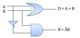
Half Subtractors
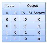
Half subtractor is a combination circuit with two inputs and two outputs (difference and borrow). It produces the difference between the two binary bits at the input and also produces a output (Borrow) to indicate if a 1 has been borrowed. In the subtraction (A-B), A is called as Minuend bit and B is called as Subtrahend bit.
Truth Table
Circuit Diagram
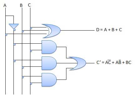
Full Subtractors
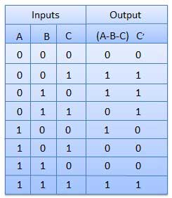
The disadvantage of a half subtractor is overcome by full subtractor. The full subtractor is a combinational circuit with three inputs A,B,C and two output D and C'. A is the minuend, B is subtrahend, C is the borrow produced by the previous stage, D is the difference output and C' is the borrow output.
Truth Table
Circuit Diagram
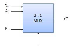
Multiplexers
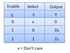
Multiplexer is a special type of combinational circuit. There are n-data inputs, one output and m select inputs with 2m = n. It is a digital circuit which selects one of the n data inputs and routes it to the output. The selection of one of the n inputs is done by the selected inputs. Depending on the digital code applied at the selected inputs, one out of n data sources is selected and transmitted to the single output Y. E is called the strobe or enable input which is useful for the cascading. It is generally an active low terminal, that means it will perform the required operation when it is low.
Block diagram
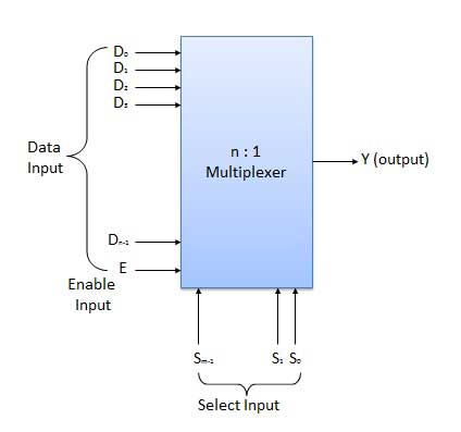
Multiplexers come in multiple variations
2 : 1 multiplexer
4 : 1 multiplexer
16 : 1 multiplexer
32 : 1 multiplexer
Block Diagram
Truth Table
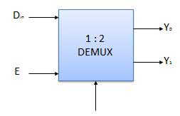
Demultiplexers
A demultiplexer perform the reverse operation of a multiplexer i.e. it receives one input and distributes it over several outputs. It has only one input, n outputs, m select input. At a time only one output line is selected by the select lines and the input is transmitted to the selected output line. A de-multiplexer is equivalent to a single pole multiple way switch as shown in fig.
Demultiplexers come in multiple variations
1 : 2 demultiplexer
1 : 4 demultiplexer
1 : 16 demultiplexer
1 : 32 demultiplexer
Block diagram
Truth Table
Decoder
A decoder is a combinational circuit. It has n input and to a maximum m = 2n outputs. Decoder is identical to a demultiplexer without any data input. It performs operation which are exactly opposite to those of an encoder.
Block diagram
Examples of Decoders are following.
Code converters
BCD to seven segment decoders
Nixie tube decoders
Relay actuator
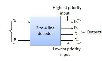
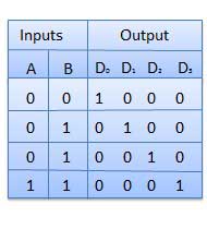
2 to 4 Line Decoder
The block diagram of 2 to 4 line decoder is shown in the fig. A and B are the two inputs where D through D are the four outputs.The truth table which explains the operation of the decoder. It shows that each output is 1 for only a specific combination of inputs.
Block diagram
Truth Table
Logic Circuit
Encoder
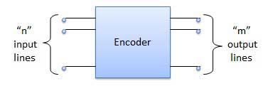
Encoder is a combinational circuit which is designed to perform the inverse operation of the decoder. An encoder has n number of input lines and m number of output lines. An encoder produces an m bit binary code corresponding to the digital input number. The encoder accepts an n input digital word and converts it into an m bit another digital word.
Block diagram
Examples of Encoders are following.
Priority encoders
Decimal to BCD encoder
Octal to binary encoder
Hexadecimal to binary encoder
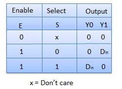
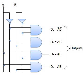
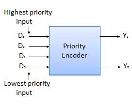
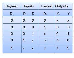
Priority Encoder
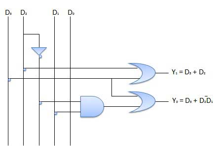
This is a special type of encoder. Priority are given to the input lines. If two or more input line are 1 at the same time, then the input line with highest priority will be considered. There are four input D0, D1, D2, D3 and two output Y0, Y1. Out of the four input D3 has the highest priority and D0 has the lowest priority. That means if D3 = 1 then Y1 Y1 = 11 irrespective of the other inputs. Similarly if D3 = 0 and D2 = 1 then Y1 Y0 = 10 irrespective of the other inputs.
Block diagram
Truth Table
Logic Circuit
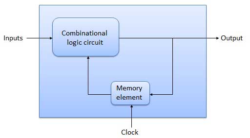
Sequential Circuits
The combinational circuit do not use any memory. Hence the previous state of input does not have any effect on the present state of the circuit. But sequential circuit has memory so output can vary based on input. This type of circuits use previous input , output ,clock and a memory element.
Block diagram
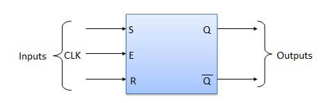
Flip Flop
Flip flop is a sequential circuit which generally samples its inputs and changes its outputs only at a particular instants of time and not continuously. Flip flop is said to be edge sensitive or edge triggered rather than being level triggered like latches.
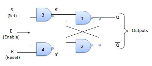
S-R Flip Flop
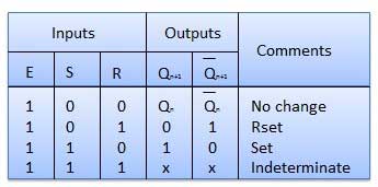
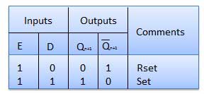
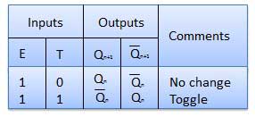
It is basically S-R latch using NAND gates with an additional enable input. It is also called as level triggered SR-FF. For this circuit in output will take place if and only if the enable input (E) is made active. In short this circuit will operate as an S-R latch if E= 1 but there is no change in the output if E = 0.
Block Diagram
Circuit Diagram
Truth Table
Operation
| S.N. | Condition | Operation |
|---|---|---|
| 1 | S = R = 0 : No change |
|
| 2 | S = 0, R = 1, E = 1 |
|
| 3 | S = 1, R = 0, E = 1 |
|
| 4 | S = 1, R = 1, E = 1 |
|
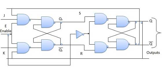
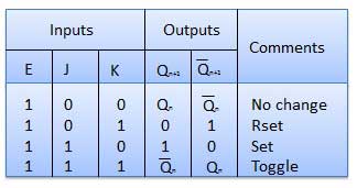
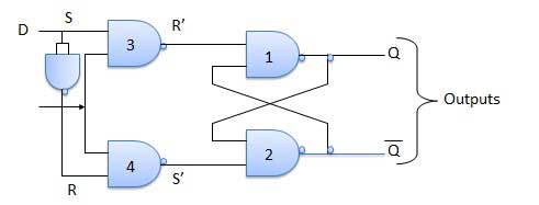
Master Slave JK Flip Flop
Master slave JK FF is a cascade of two S-R FF with feedback from the output of second to input of first. Master is a positive level triggered. But due to the presence of the inverter in the clock line, the slave will respond to the negative level. Hence when the clock = 1 (positive level) the master is active and the slave is inactive. Whereas when clock = 0 (low level) the slave is active and master is inactive.
Circuit Diagram
Truth Table
Operation
| S.N. | Condition | Operation |
|---|---|---|
| 1 | J = K = 0 (No change) |
|
| 2 | J = 0 and K = 1 (Reset) |
|
| 3 | J = 1 and K = 0 (Set) |
|
| 4 | J = K = 1 (Toggle) |
|
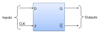
Deplay Flip Flop / D Flip Flop
Delay Flip Flop or D Flip Flop is the simple gated S-R latch with a NAND inverter connected between S and R inputs. It has only one input. The input data is appear at the output after some time. Due to this data delay between i/p and o/p, it is called delay flip flop. S and R will be the complements of each other due to NAND inverter. Hence S = R = 0 or S = R = 1,these input condition will never apper.This problem is avoid by SR = 00 and SR = 1 conditions.
Block Diagram
Circuit Diagram
Truth Table
Operation
| S.N. | Condition | Operation |
|---|---|---|
| 1 | E = 0 |
|
| 2 | E = 1 and D = 0 |
|
| 3 | E = 1 and D = 1 |
|
Toggle Flip Flop / T Flip Flop
Toggle flip flop is basically a JK flip flop with J and K terminals permanently connected together. It has only input denoted by T is shown in the Symbol Diagram. The symbol for positive edge triggered T flip flop is shown in the Block Diagram.
Symbol Diagram
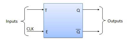
Block Diagram
Truth Table
Operation
| S.N. | Condition | Operation |
|---|---|---|
| 1 | T = 0, J = K = 0 |
|
| 2 | T = 1 ,J = K = 1 |
|
Digital Registers
Flip-flop is a 1 bit memory cell which can be used for storing the digital data. To increase the storage capacity in terms of number of bits, we have to use a group of flip-flop. Such a group of flip-flop is known as a Register. The n-bit register will consist of n number of flip-flop and it is capable of storing an n-bit word.
The binary data in a register can be moved within the register from one flip-flop to another. The registers that allow such data transfers are called as shift registers. There are four mode of opearation of a shift register.
Serial Input Serial Output
Serial Input Parallel Output
Parallel Input Serial Output
Parallel Input Parallel Output
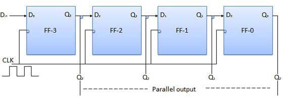
Serial Input Serial Output
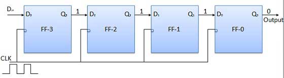
Let all the flip-flop be initially in the reset condition i.e. Q3 = Q2 = Q1 = Q0 = 0. If we entry of a four bit binary number 1 1 1 1 into the register. When this is to be done, this number should be applied to Din bit by with the LSB bit applied first. The D input of FF-3 i.e. D3 is connected to serial data input Din. Output of FF-3 i.e. Q3 is connected to the input of the next flip-flop i.e. D2 and so on.
Block Diagram
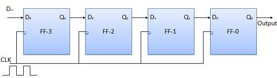
Operation
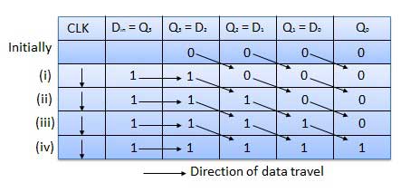
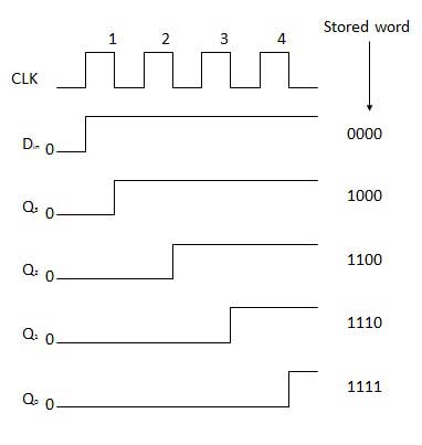
Before application of clock signal let Q3 Q2 Q1 Q0 = 0000 and apply LSB bit of the number to be entered to Din. So Din=D3=1. Apply the clock. On the first falling edge of clock, the FF-3 is set, and stored word in the register is Q3 Q2 Q1 Q0 = 1000.
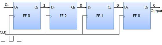
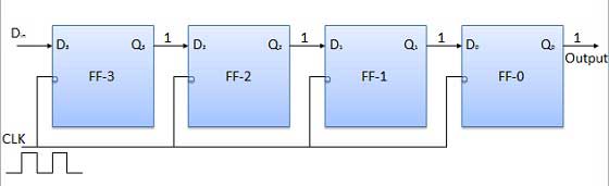
Apply the next bit to Din. So Din=1. As soon as the next negative edge of the clock hits, FF-2 will set and the stored word change to Q3 Q2 Q1 Q0 = 1100.
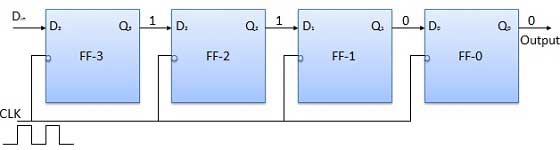
Apply the next bit to be stored i.e. 1 to Din. Apply the clock pulse. As soon as the third negative clock edge hits, FF-1 will be set and output will be modified to Q3 Q2 Q1 Q0 = 1110.
Similarly with Din=1 and with the fourth negative clock edge arriving, the stored word in the register is Q3 Q2 Q1 Q0 = 1111.
Truth Table
Waveforms
Serial Input Parallel Output
In such types of operations, the data is entered serially and taken out in parallel fashion.
Data is loaded bit by bit. The outputs are disabled as long as the data is loading.
As soon as the data loading gets completed, all the flip-flops contain their required data, the outputs are enabled so that all the loaded data is made available over all the output lines at the same time.
4 clock cycles are required to load a four bit word. Hence the speed of operation of SIPO mode is same as that of SISO mode.
Block Diagram
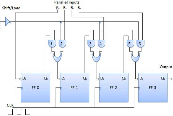
Parallel Input Serial Output (PISO)
Data bits are entered in parallel fashion.
The circuit shown below is a four bit parallel input serial output register.
Output of previous Flip Flop is connected to the input of the next one via a combinational circuit.
The binary input word B0,B1,B2,B3 is applied though the same combinational circuit.
There are two modes in which this circuit can work namely shift mode or load mode.
Load mode
When the shift/load bar line is low (0), the AND gate 2,4 and 6 become active. They will pass B1,B2,B3 bits to the corresponding flip-flops. On the low going edge of clock, the binary input B0,B1,B2,B3 will get loaded into the corresponding flip-flops. Thus parallel loading takes place.
Shift mode
When the shift/load bar line is low (1), the AND gate 2,4 and 6 become inactive. Hence the parallel loading of the data becomes impossible. But the AND gate 1,3 and 5 become active. Therefore the shifting of data from left to right bit by bit on application of clock pulses. Thus the parallel in serial out operation take place.
Block Diagram
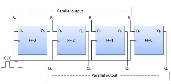
Parallel Input Parallel Output (PIPO)
In this mode, the 4 bit binary input B0,B1,B2,B3 is applied to the data inputs D0,D1,D2,D3 respectively of the four flip-flops. As soon as a negative clock edge is applied, the input binary bits will be loaded into the flip-flops simultaneously. The loaded bits will appear simultaneously to the output side. Only clock pulse is essential to load all the bits.
Block Diagram
Bidirectional Shift Register
If a binary number is shifted left by one position then it is equivalent to multiplying the original number by 2. Similarly if a binary number is shifted right by one position then it is equivalent to dividing the original number by 2.
Hence if we want to use the shift register to multiply and divide the given binary number, then we should be able to move the data in either left or right direction.
Such a register is called as a bi-directional register. A four bit bi-directional shift register is shown in fig.
There are two serial inputs namely the serial right shift data input DR and the serial left shift data input DL along with a mode select input (M).
Block Diagram
Operation
| S.N. | Condition | Operation |
|---|---|---|
| 1 | With M = 1 : Shift right operation |
|
| 2 | With M = 0 : Shift left operation |
|
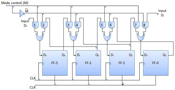
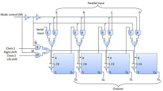
Universal Shift Register
A shift register which can shift the data in only one direction is called a uni-directional shift register. A shift register which can shift the data in both directions is called a bi-directional shift register. Applying the same logic, a shift register which can shift the data in both directions as well as load it parallely, then it is known as a universal shift register. The shift register is capable of performing the following operation
Parallel loading
Lift shifting
Right shifting
The mode control input is connected to logic 1 for parallel loading operation whereas it is connected to 0 for serial shifting. With mode control pin connected to ground, the universal shift register acts as a bi-directional register. For serial left operation, the input is applied to the serial input which goes to AND gate-1 shown in figure. Whereas for the shift right operation, the serial input is applied to D input.
Block Diagram
Digital Counters
Counter is a sequential circuit. A digital circuit which is used for a counting pulses is known counter. Counter is the widest application of flip-flops. It is a group of flip-flops with a clock signal applied. Counters are of two types.
Asynchronous or ripple counters
Synchronous counters.
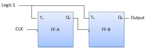
Asynchronous or ripple counters
The logic diagram of a 2-bit ripple up counter is shown in figure. The toggle(T) flip-flop are being used. But we can use the JK flip-flop also with J and K connected permanently to logic 1. External clock is applied to the clock input of flip-flop A and QA output is applied to the clock input of the next flip-flop i.e. FF-B.
Logical Diagram
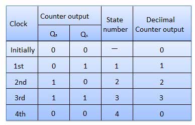
Operation
| S.N. | Condition | Operation |
|---|---|---|
| 1 | Initially let both the FFs be in the reset state | QBQA = 00................initially |
| 2 | After 1st negative clock edge |
QBQA = 01................After the first clock pulse |
| 3 | After 2nd negative clock edge |
QBQA = 10................After the second clock pulse |
| 4 | After 3rd negative clock edge |
QBQA = 11................After the third clock pulse |
| 5 | After 4th negative clock edge |
QBQA = 00................After the fourth clock pulse |
Truth Table
Synchronous counters
If the "clock" pulses are applied to all the flip-flops in a counter simultaneously, then such a counter is called as synchronous counter.
2-bit Synchronous up counter
The JA and KA inputs of FF-A are tied to logic 1. So FF-A will work as a toggle flip-flop. The JB and KB inputs are connected to QA.
Logical Diagram
Operation
| S.N. | Condition | Operation |
|---|---|---|
| 1 | Initially let both the FFs be in the reset state | QBQA = 00................initially |
| 2 | After 1st negative clock edge |
QBQA = 01................After the first clock pulse |
| 3 | After 2nd negative clock edge |
QBQA = 10................After the second clock pulse |
| 4 | After 3rd negative clock edge |
QBQA = 11................After the third clock pulse |
| 5 | After 4th negative clock edge |
QBQA = 00................After the fourth clock pulse |
Classification of counters
Depending on the way in which the counting progresses, the synchronous or asynchronous counters are classified as follows.
Up counters
Down counters
Up/Down counters
UP/DOWN Counter
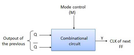
In the up/down counter, when up counter and down counter combined together to obtain an UP/DOWN counter. A mode control (M) input is also provided to select either up or down mode. A combinational circuit is required to be designed and used between each pair of flip-flop in order to achieve the up/down operation.
Type of up/down counters
UP/DOWN ripple counters
UP/DOWN synchronous counters
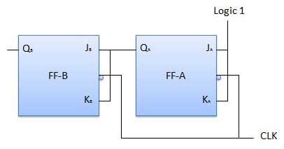
UP/DOWN Ripple Counters
In the UP/DOWN ripple counter all the FFs operate in the toggle mode. So either T flip-flops or JK flip-flops are to be used. The LSB flip-flop receives clock directly. But the clock to every other FF is obtained from (Q = Q bar) output of the previous FF.
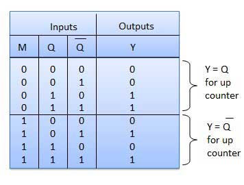
UP counting mode (M=0) - The Q output of the preceding FF is connected to the clock of the next stage if up counting is to be achieved. For this mode, the mode select input M is at logic 0 (M=0).
DOWN counting mode (M=1) - If M =1, then the Q bar output of the preceding FF is connected to the next FF. This will operate the counter in the counting mode.
Example
3-bit binary up/down ripple counter.
3-bit : hence three FFs are required.
UP/DOWN : So a mode control input is essential.
For a ripple up counter, the Q output of preceding FF is connected to the clock input of the next one.
For a ripple up counter, the Q output of preceding FF is connected to the clock input of the next one.
For a ripple down counter, the Q bar output of preceding FF is connected to the clock input of the next one.
Let the selection of Q and Q bar output of the preceding FF be controlled by the mode control input M such that, If M = 0, UP counting. So connect Q to CLK. If M = 1, DOWN counting. So connect Q bar to CLK
Block Diagram
Truth Table
Operation
| S.N. | Condition | Operation |
|---|---|---|
| 1 | Case 1: With M = 0 (Up counting mode) |
|
| 2 | Case 2: With M = 1 (Down counting mode) |
|
Modulus Counter (MOD-N Counter)
The 2-bit ripple counter is called as MOD-4 counter and 3-bit ripple counter is called as MOD-8 counter. So in general, an n-bit ripple counter is called as modulo-N counter. Where,MOD number = 2n
Type of modulus
2-bit up or down (MOD-4)
3-bit up or down (MOD-8)
4-bit up or down (MOD-16)
Application of the counters
Frequency counters
Digital clock
Time measurement
A to D converter
Frequency divider circuits
Digital triangular wave generator
Memory Devices
A memory is just like a human brain. It is used to store data and instruction. Computer memory is the storage space in computer where data is to be processed and instructions required for processing are stored.
The memory is divided into large number of small parts. Each part is called cell. Each location or cell has a unique address which varies from zero to memory size minus one.
For example if computer has 64k words, then this memory unit has 64 * 1024=65536 memory location. The address of these locations varies from 0 to 65535.
Memory is primarily of two types
Internal Memory - cache memory and primary/main memory
External Memory - magnetic disk / optical disk etc.
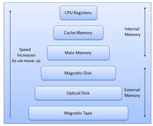
Characteristics of Memory Hierarchy are following when we go from top to bottom.
Capacity in terms of storage increases.
Cost per bit of storage decreases.
Frequency of access of the memory by the CPU decreases.
Access time by the CPU increases
RAM
A RAM constitutes the internal memory of the CPU for storing data, program and program result. It is read/write memory. It is called random access memory (RAM).
Since access time in RAM is independent of the address to the word that is, each storage location inside the memory is as easy to reach as other location & takes the same amount of time. We can reach into the memory at random & extremely fast but can also be quite expensive.
RAM is volatile, i.e. data stored in it is lost when we switch off the computer or if there is a power failure. Hence a backup uninterruptible power system(UPS) is often used with computers. RAM is small , both in terms of its physical size and in the amount of data it can hold.
RAM is of two types
Static RAM (SRAM)
Dynamic RAM (DRAM)
Static RAM (SRAM)
The word static indicates that the memory retains its contents as long as power remains applied. However, data is lost when the power gets down due to volatile nature. SRAM chips use a matrix of 6-transistors and no capacitors. Transistors do not require power to prevent leakage, so SRAM need not have to be refreshed on a regular basis.
Because of the extra space in the matrix, SRAM uses more chips than DRAM for the same amount of storage space, thus making the manufacturing costs higher.
Static RAM is used as cache memory needs to be very fast and small.
Dynamic RAM (DRAM)
DRAM, unlike SRAM, must be continually refreshed in order for it to maintain the data. This is done by placing the memory on a refresh circuit that rewrites the data several hundred times per second. DRAM is used for most system memory because it is cheap and small. All DRAMs are made up of memory cells. These cells are composed of one capacitor and one transistor.
ROM
ROM stands for Read Only Memory. The memory from which we can only read but cannot write on it. This type of memory is non-volatile. The information is stored permanently in such memories during manufacture.
A ROM, stores such instruction as are required to start computer when electricity is first turned on, this operation is referred to as bootstrap. ROM chip are not only used in the computer but also in other electronic items like washing machine and microwave oven.
Following are the varioys types of ROM
MROM (Masked ROM)
The very first ROMs were hard-wired devices that contained a pre-programmed set of data or instructions. These kind of ROMs are known as masked ROMs. It is inexpensive ROM.
PROM (Programmable Read only Memory)
PROM is read-only memory that can be modified only once by a user. The user buys a blank PROM and enters the desired contents using a PROM programmer.Inside the PROM chip there are small fuses which are burnt open during programming. It can be programmed only once and is not erasable.
EPROM(Erasable and Programmable Read Only Memory)
The EPROM can be erased by exposing it to ultra-violet light for a duration of upto 40 minutes. Usually, a EPROM eraser achieves this function. During programming an electrical charge is trapped in an insulated gate region. The charge is retained for more than ten years because the charge has no leakage path. For erasing this charge, ultra-violet light is passed through a quartz crystal window(lid). This exposure to ultra-violet light dissipates the charge. During normal use the quartz lid is sealed with a sticker.
EEPROM(Electrically Erasable and Programmable Read Only Memory)
The EEPROM is programmed and erased electrically. It can be erased and reprogrammed about ten thousand times. Both erasing and programming take about 4 to 10 ms (milli second). In EEPROM, any location can be selectively erased and programmed. EEPROMs can be erased one byte at a time, rather than erasing the entire chip. Hence, the process of re-programming is flexible but slow.
Serial Access Memory
Sequential access means the system must search the storage device from the beginning of the memory address until it finds the required piece of data. Memory device which supports such access is called a Sequential Access Memory or Serial Access Memory. Magnetic tape is an example of serial access memory.
Direct Access Memory
Direct access memory or Random Access Memory, refers to condition in which a system can go directly to the information that the user wants. Memory device which supports such access is called a Direct Access Memory. Magnetic disk, optical disks are an examples of direct access memory.
Cache Memory
Cache memory is a very high speed semiconductor memory which can speed up CPU. It acts as a buffer between the CPU and main memory. It is used to hold those parts of data and program which are most frequently used by CPU. The parts of data and programs are transferred from disk to cache memory by operating system, from where CPU can access them.
Advantages
Cache memory is faster than main memory.
It consumes less access time as compared to main memory.
It stores the program that can be executed within a short period of time.
It stores data for temporary use.
Disadvantages
Cache memory has limited capacity.
It is very expensive.
Virtual memory is a technique that allows the execution of processes which are not completely available in memory. The main visible advantage of this scheme is that programs can be larger than physical memory. Virtual memory is the separation of user logical memory from physical memory.
This separation allows an extremely large virtual memory to be provided for programmers when only a smaller physical memory is available. Following are the situations, when entire program is not required to be loaded fully in main memory.
User written error handling routines are used only when an error occured in the data or computation.
Certain options and features of a program may be used rarely.
Many tables are assigned a fixed amount of address space even though only a small amount of the table is actually used.
The ability to execute a program that is only partially in memory would counter many benefits.
Less number of I/O would be needed to load or swap each user program into memory.
A program would no longer be constrained by the amount of physical memory that is available.
Each user program could take less physical memory, more programs could be run the same time, with a corresponding increase in CPU utilization and throughput.
Auxiliary Memory
Auxiliary memory is much larger in size than main memory but is slower. It normally stores system programs, instruction and data files. It is also known as secondary memory. It can also be used as an overflow/virtual memory in case the main memory capacity has been exceeded. Secondary memories can not be accessed directly by a processor. First the data / information of auxillary memory is transferred to the main memory and then that information can be accessed by the CPU. Characteristics of Auxiliary Memory are following
Non-volatile memory - Data is not lost when power is cut off.
Reusable - The data stays in the secondary storage on permanent basis until it is not overwritten or deleted by the user.
Reliable - Data in secondary storage is safe because of high physical stability of secondary storage device.
Convenience - With the help of a computer software, authorised people can locate and access the data quickly.
Capacity - Secondary storage can store large volumes of data in sets of multiple disks.
Cost - It is much lesser expensive to store data on a tape or disk than primary memory.
