- Digital Electronics - Home
- Digital Electronics Basics
- Types of Digital Systems
- Types of Signals
- Logic Levels And Pulse Waveforms
- Digital System Components
- Digital Logic Operations
- Digital Systems Advantages
- Number Systems
- Number Systems
- Binary Numbers Representation
- Binary Arithmetic
- Signed Binary Arithmetic
- Octal Arithmetic
- Hexadecimal Arithmetic
- Complement Arithmetic
- Base Conversions
- Base Conversions
- Binary to Decimal Conversion
- Decimal to Binary Conversion
- Binary to Octal Conversion
- Octal to Binary Conversion
- Octal to Decimal Conversion
- Decimal to Octal Conversion
- Hexadecimal to Binary Conversion
- Binary to Hexadecimal Conversion
- Hexadecimal to Decimal Conversion
- Decimal to Hexadecimal Conversion
- Octal to Hexadecimal Conversion
- Hexadecimal to Octal Conversion
- Binary Codes
- Binary Codes
- 8421 BCD Code
- Excess-3 Code
- Gray Code
- ASCII Codes
- EBCDIC Code
- Code Conversion
- Error Detection & Correction Codes
- Logic Gates
- Logic Gates
- AND Gate
- OR Gate
- NOT Gate
- Universal Gates
- XOR Gate
- XNOR Gate
- CMOS Logic Gate
- OR Gate Using Diode Resistor Logic
- AND Gate vs OR Gate
- Two Level Logic Realization
- Threshold Logic
- Boolean Algebra
- Boolean Algebra
- Laws of Boolean Algebra
- Boolean Functions
- DeMorgan's Theorem
- SOP and POS Form
- POS to Standard POS Form
- Minimization Techniques
- K-Map Minimization
- Three Variable K-Map
- Four Variable K-Map
- Five Variable K-Map
- Six Variable K-Map
- Don't Care Condition
- Quine-McCluskey Method
- Min Terms and Max Terms
- Canonical and Standard Form
- Max Term Representation
- Simplification using Boolean Algebra
- Combinational Logic Circuits
- Digital Combinational Circuits
- Digital Arithmetic Circuits
- Multiplexers
- Multiplexer Design Procedure
- Mux Universal Gate
- 2-Variable Function Using 4:1 Mux
- 3-Variable Function Using 8:1 Mux
- Demultiplexers
- Mux vs Demux
- Parity Bit Generator and Checker
- Comparators
- Encoders
- Keyboard Encoders
- Priority Encoders
- Decoders
- Arithmetic Logic Unit
- 7-Segment LED Display
- Code Converters
- Code Converters
- Binary to Decimal Converter
- Decimal to BCD Converter
- BCD to Decimal Converter
- Binary to Gray Code Converter
- Gray Code to Binary Converter
- BCD to Excess-3 Converter
- Excess-3 to BCD Converter
- Adders
- Half Adders
- Full Adders
- Serial Adders
- Parallel Adders
- Full Adder using Half Adder
- Half Adder vs Full Adder
- Full Adder with NAND Gates
- Half Adder with NAND Gates
- Binary Adder-Subtractor
- Subtractors
- Half Subtractors
- Full Subtractors
- Parallel Subtractors
- Full Subtractor using 2 Half Subtractors
- Half Subtractor using NAND Gates
- Sequential Logic Circuits
- Digital Sequential Circuits
- Clock Signal and Triggering
- Latches
- Shift Registers
- Shift Register Applications
- Binary Registers
- Bidirectional Shift Register
- Counters
- Binary Counters
- Non-binary Counter
- Design of Synchronous Counter
- Synchronous vs Asynchronous Counter
- Finite State Machines
- Algorithmic State Machines
- Flip Flops
- Flip-Flops
- Conversion of Flip-Flops
- D Flip-Flops
- JK Flip-Flops
- T Flip-Flops
- SR Flip-Flops
- Clocked SR Flip-Flop
- Unclocked SR Flip-Flop
- Clocked JK Flip-Flop
- JK to T Flip-Flop
- SR to JK Flip-Flop
- Triggering Methods:Flip-Flop
- Edge-Triggered Flip-Flop
- Master-Slave JK Flip-Flop
- Race-around Condition
- A/D and D/A Converters
- Analog-to-Digital Converter
- Digital-to-Analog Converter
- DAC and ADC ICs
- Realization of Logic Gates
- NOT Gate from NAND Gate
- OR Gate from NAND Gate
- AND Gate from NAND Gate
- NOR Gate from NAND Gate
- XOR Gate from NAND Gate
- XNOR Gate from NAND Gate
- NOT Gate from NOR Gate
- OR Gate from NOR Gate
- AND Gate from NOR Gate
- NAND Gate from NOR Gate
- XOR Gate from NOR Gate
- XNOR Gate from NOR Gate
- NAND/NOR Gate using CMOS
- Full Subtractor using NAND Gate
- AND Gate Using 2:1 MUX
- OR Gate Using 2:1 MUX
- NOT Gate Using 2:1 MUX
- Memory Devices
- Memory Devices
- RAM and ROM
- Cache Memory Design
- Programmable Logic Devices
- Programmable Logic Devices
- Programmable Logic Array
- Programmable Array Logic
- Field Programmable Gate Arrays
- Digital Electronics Families
- Digital Electronics Families
- CPU Architecture
- CPU Architecture
CPU Architecture
Microprocessing unit is synonymous to central processing unit, CPU used in traditional computer. Microprocessor (MPU) acts as a device or a group of devices which do the following tasks.
- Communicate with peripherals devices
- Provide timing signal
- Direct data flow
- Perform computer tasks as specified by the instructions in memory
8085 Microprocessor
The 8085 microprocessor is an 8-bit general purpose microprocessor which is capable to address 64k of memory. This processor has forty pins, requires +5 V single power supply and a 3-MHz single-phase clock.
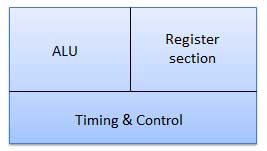
Block Diagram

ALU
The ALU perform the computing function of microprocessor. It includes the accumulator, temporary register, arithmetic & logic circuit & and five flags. Result is stored in accumulator & flags.
Block Diagram
Accumulator
It is an 8-bit register that is part of ALU. This register is used to store 8-bit data & in performing arithmetic & logic operation. The result of operation is stored in accumulator.
Diagram
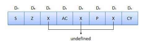
Flags
Flags are programmable. They can be used to store and transfer the data from the registers by using instruction. The ALU includes five flip-flops that are set and reset according to data condition in accumulator and other registers.
- S (Sign) flag − After the execution of an arithmetic operation, if bit D7 of the result is 1, the sign flag is set. It is used to signed number. In a given byte, if D7 is 1 means negative number. If it is zero means it is a positive number.
- Z (Zero) flag − The zero flag is set if ALU operation result is 0.
- AC (Auxiliary Carry) flag − In arithmetic operation, when carry is generated by digit D3 and passed on to digit D4, the AC flag is set. This flag is used only internally BCD operation.
- P (Parity) flag − After arithmetic or logic operation, if result has even number of 1s, the flag is set. If it has odd number of 1s, flag is reset.
- C (Carry) flag − If arithmetic operation result is in a carry, the carry flag is set, otherwise it is reset.
Register Section
It is basically a storage device and transfers data from registers by using instructions.
- Stack Pointer (SP) − The stack pointer is also a 16-bit register which is used as a memory pointer. It points to a memory location in Read/Write memory known as stack. In between execution of program, sometime data to be stored in stack. The beginning of the stack is defined by loading a 16-bit address in the stack pointer.
- Program Counter (PC) − This 16-bit register deals with fourth operation to sequence the execution of instruction. This register is also a memory pointer. Memory location have 16-bit address. It is used to store the execution address. The function of the program counter is to point to memory address from which next byte is to be fetched.
- Storage registers − These registers store 8-bit data during a program execution. These registers are identified as B, C, D, E, H, L. They can be combined as register pair BC, DE and HL to perform some 16 bit operations.
Time and Control Section
This unit is responsible to synchronize Microprocessor operation as per the clock pulse and to generate the control signals which are necessary for smooth communication between Microprocessor and peripherals devices. The RD bar and WR bar signals are synchronous pulses which indicates whether data is available on the data bus or not. The control unit is responsible to control the flow of data between microprocessor, memory and peripheral devices.
PIN Diagram
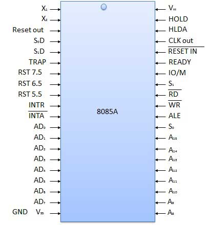
All the signal can be classified into six groups
| Sr.No | Group | Description |
|---|---|---|
| 1 | Address bus | The 8085 microprocessor has 8 signal line, A15 - A8 which are uni directional and used as a high order address bus. |
| 2 | Data bus | The signal line AD7 - AD0 are bi-directional for dual purpose. They are used as low order address bus as well as data bus. |
| 3 | Control signal and Status signal |
Control Signal RD bar − It is a read control signal (active low). If it is active then memory read the data. WR bar − It is write control signal (active low). It is active when written into selected memory. Status signal ALE (Address Latch Enable) − When ALE is high. 8085 microprocessor use address bus. When ALE is low. 8085 microprocessor is use data bus. IO/M bar − This is a status signal used to differentiate between i/o and memory operations. When it is high, it indicate an i/o operation and when it is low, it indicate memory operation. S1 and S0 − These status signals, similar to i/o and memory bar, can identify various operations, but they are rarely used in small system. |
| 4 | Power supply and frequency signal |
Vcc − +5v power supply. Vss − ground reference. X, X − A crystal is connected at these two pins. The frequency is internally divided by two operate system at 3-MHz, the crystal should have a frequency of 6-MHz. CLK out − This signal can be used as the system clock for other devices. |
| 5 | Externally initiated signal |
INTR (i/p) − Interrupt request. INTA bar (o/p) − It is used as acknowledge interrupt. TRAP (i/p) − This is non maskable interrupt and has highest priority. HOLD (i/p) − It is used to hold the executing program. HLDA (o/p) − Hold acknowledge. READY (i/p) − This signal is used to delay the microprocessor read or write cycle until a slow responding peripheral is ready to accept or send data. RESET IN bar − When the signal on this pin goes low, the program counter is set to zero, the bus are tri-stated, & MPU is reset. RESET OUT − This signal indicate that MPU is being reset. The signal can be used to reset other devices. RST 7.5, RST 6.5, RST 5.5 (Request interrupt) − It is used to transfer the program control to specific memory location. They have higher priority than INTR interrupt. |
| 6 | Serial I/O ports | The 8085 microprocessor has two signals to implement the serial transmission serial input data and serial output data. |
Instruction Format
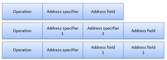
Each instruction is represented by a sequence of bits within the computer. The instruction is divided into group of bits called field. The way instruction is expressed is known as instruction format. It is usually represented in the form of rectangular box. The instruction format may be of the following types.
Variable Instruction Formats
These are the instruction formats in which the instruction length varies on the basis of opcode & address specifiers. For Example, VAX instruction vary between 1 and 53 bytes while X86 instruction vary between 1 and 17 bytes.
Format

Advantage
These formats have good code density.
Drawback
These instruction formats are very difficult to decode and pipeline.
Fixed Instruction Formats
In this type of instruction format, all instructions are of same size. For Example, MIPS, Power PC, Alpha, ARM.
Format

Advantage
They are easy to decode & pipeline.
Drawback
They don't have good code density.
Hybrid Instruction Formats
In this type of instruction formats, we have multiple format length specified by opcode. For example, IBM 360/70, MIPS 16, Thumb.
Format
Advantage
These compromise between code density & instruction of these type are very easy to decode.
Addressing Modes
Addressing mode provides different ways for accessing an address to given data to a processor. Operated data is stored in the memory location, each instruction required certain data on which it has to operate. There are various techniques to specify address of data. These techniques are called Addressing Modes.
- Direct Addressing Mode − In the direct addressing mode, address of the operand is given in the instruction and data is available in the memory location which is provided in instruction. We will move this data in desired location.
- Indirect Addressing Mode − In the indirect addressing mode, the instruction specifies a register which contain the address of the operand. Both internal RAM and external RAM can be accessed via indirect addressing mode.
- Immediate addressing Mode − In the immediate addressing mode, direct data is given in the operand which move the data in accumulator. It is very fast.
- Relative Addressing Mode − In the relative address mode, the effective address is determined by the index mode by using the program counter in stead of general purpose processor register. This mode is called relative address mode.
- Index Addressing Mode − In the index address mode, the effective address of the operand is generated by adding a content value to the contents of the register. This mode is called index address mode.
