
Article Categories
- All Categories
-
 Data Structure
-
 Networking
-
 RDBMS
RDBMS
-
 Operating System
-
 Java
Java
-
 MS Excel
-
 iOS
iOS
-
 HTML
HTML
-
 CSS
CSS
-
 Android
-
 Python
-
 C Programming
-
 C++
C++
-
 C#
C#
-
 MongoDB
-
 MySQL
MySQL
-
 Javascript
-
 PHP
PHP
-
 Economics & Finance
Build an Inverter with a Transistor
In this tutorial, we will discuss the realization of an inverter (NOT gate) with a transistor. But before that let's have a look into the basics of inverter or NOT gate.
What is an Inverter (NOT Gate)?
An inverter is a single input and single output logic gate that toggles or inverts the logic level (or state) of a single to the opposite state or logic level. The inverter is also known as NOT gate.
When a low signal (logic 0) is applied to an inverter, it transforms it to a high signal (logic 1). If a high signal (logic 1) is applied to the inverter, then it converts it to a low signal (logic 0). Thus, the inverter (NOT gate) alters the logic state of the input signal to its opposite logic state.

Therefore, an inverter is basically a device whose output is always the inversion (or complement) of its input. The standard symbol of the inverter is shown in figure-1. The NOT operation is often represented by a bar (-) symbol. Thus, if A is the input variable to the inverter and Y is the output variable of the inverter, then the expression for the output of the inverter is given by,
$$\mathrm{Y=\bar{A}}$$
It is read as Y is equal to A bar.
Truth Table of NOT Gate (Inverter)
The following is the truth table of the NOT gate (inverter) ?
Input (A) |
Output (Y = A') |
|---|---|
0 |
1 |
1 |
0 |
We can realize an inverter in many ways like using OR gate, AND gate, NAND gate, NOR gate, etc. An inverter may also be created using a transistor, which will discuss in this article.
Build an Inverter with a Transistor
As we known, a transistor can function as a switch, i.e., ON switch in its saturation state and OFF switch in its cut off state. Due to this characteristic of the transistor, we may use it as a switch to perform inversion (NOT gate) operation. The circuit diagram of a transistor inverter is shown in Figure-2.
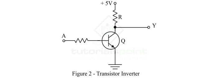
Here, we used the transistor in its common emitter configuration. In the common emitter configuration, the transistor provides a phase shift of 180° between input and output. Due to this 180° phase shift, the transistor can produce a high signal (logic 1) at the output when the applied input is low, and it can produce a low signal (logic 0) at the output when the applied input is high. In this way, a transistor work like an inverter and produces inverted value at the output.
Operation and Truth Table of Transistor Inverter
The input to the transistor inverter may be 0 V or +5 V. Thus, when the input A is at 0 V, the transistor Q is OFF. Therefore, no current flows through the resistor R, and hence there is no voltage drop across it. As a result, the output voltage Y = +5 V. When A = +5 V, the transistor Q is ON and the output voltage Y = 0 V. The truth table for the transistor inverter is shown below.
Input (A) |
Output (Y) |
|---|---|
0 V |
5 V |
5 V |
0 V |
Hence, in this way, we can build an inverter with a transistor. Where, the transistor is used in the common emitter configuration.

9K+ Views
