
Article Categories
- All Categories
-
 Data Structure
-
 Networking
-
 RDBMS
RDBMS
-
 Operating System
-
 Java
Java
-
 MS Excel
-
 iOS
iOS
-
 HTML
HTML
-
 CSS
CSS
-
 Android
-
 Python
-
 C Programming
-
 C++
C++
-
 C#
C#
-
 MongoDB
-
 MySQL
MySQL
-
 Javascript
-
 PHP
PHP
-
 Economics & Finance
Basic MOS Transistors
MOS stands for Metal Oxide Semiconductor. Metal Oxide Semiconductor is used for constructing transistors which are called MOSFET (Metal Oxide Semiconductor Field Effect Transistors). MOS transistors are being extensively used in a variety of modern electronic and power electronic devices like inverters, microprocessors, memory ICs, digital logic circuits, and more.
What is a MOS Transistor?
A MOS (Metal Oxide Semiconductor) transistor is a type of field effect transistor (FET) that can operate in both depletion mode and enhancement mode. A MOS transistor typically consists of three-terminals namely, Gate (G), Source (S), and Drain (D). The major parts of a MOS transistor are: a semiconductor channel, an oxide insulating layer, a metal gate, and terminals.
The most important point to know about MOS transistor is that it is a voltage-controlled device which means the operation or current flow through the semiconductor channel is controlled by varying the voltage applied to the gate terminal.
In the MOS transistor, the gate terminal is made up of metal and is separated from the semiconductor channel by an insulating layer made up of silicon dioxide. This arrangement allows the gate voltage to establish an electric field in the semiconductor channel and control its electrical conductivity.
Construction of MOS Transistor
A MOS transistor consists of a lightly dopped semiconductor substrate, two heavily dopped regions, oxide layer, and metallic gate terminal.
The basic construction of a MOS transistor is depicted in the following figure.
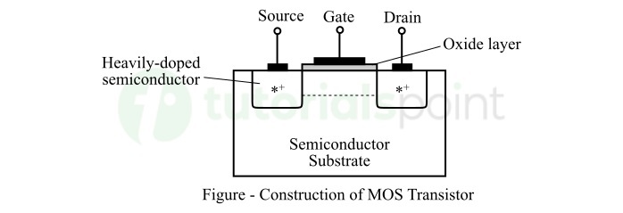
To construct a MOS transistor, a lightly dopped semiconductor substrate is taken into which two heavily doped semiconductor regions are diffused, which act as source and drain of the MOS transistor. An oxide layer made of silicon dioxide is deposited on the lightly doped semiconductor substrate to which the metallic gate terminal is attached. This oxide layer acts as an insulating layer between the metallic gate terminal and the lightly doped semiconductor substrate.
Depending on the type of semiconductor substrate used, the MOS transistors are called as PMOS and NMOS transistors.
Types of MOS Transistors
Depending on the type of semiconductor channel, there are two types of MOS transistors namely,
NMOS Transistor (N-Channel Metal Oxide Semiconductor Transistor)
PMOS Transistor (P-Channel Metal Oxide Semiconductor Transistor)
NMOS Transistor
In the case of NMOS Transistor (N-Channel Metal Oxide Semiconductor Transistor), a lightly doped P-type semiconductor substrate is diffused with a heavily doped n-type region. An insulating oxide layer is deposited on the p-type substrate to which the metallic gate terminal is connected.
The basic construction of an NMOS transistor is displayed in the following figure.

When a voltage is applied to the gate terminal, it creates an n-channel in between the source and drain. In the NMOS transistor, the heavily doped n-type regions act as source and drain.
PMOS Transistor
In the PMOS transistor, a lightly doped n-type semiconductor substrate is diffused with two heavily dopped P-type substrates, which act as source and drain. A thin layer of silicon dioxide is deposited on the surface of the n-type substrate. The basic construction of a PMOS transistor depicted in the figure below.

When a voltage is applied at the gate terminal, a p-type channel induced in the n-type substrate between the source and drain through which current flows. The current flowing through the p-channel is connected by varying the gate voltage.
Regions of Operation of MOS Transistors
MOS transistors operate in the following three regions ?
Cutoff Region ? In the cutoff region of operation, the MOS transistor remains in off state and hence, there is no current flow from source to drain. In the cutoff region, the MOS transistor acts as an open switch.
Saturation Region ? In the saturation region, the MOS transistor allows the flow of electric current between source and drain. Consequently, MOS transistor in saturation region of operation acts as a closed switch.
Linear/Ohmic Region ? In the linear region, the MOS transistor offers a constant resistance in the flow of current between source and drain. This resistance is controlled by the gate voltage. MOS transistor operating in linear region is used in amplification applications.
Working of MOS Transistors
A MOS transistor can operate as a solid-state switch or an amplifier. The operation of a MOS transistor is completely dependent on its type and biasing, i.e. a MOS transistor can operate in two modes, namely depletion mode and enhancement mode.
As mentioned above, a MOS transistor has an insulating oxide layer between the channel and the gate terminal. This oxide insulating layer increases the input impedance of the MOS transistor. Hence, it restricts the flow of gate current.
Depletion Mode Operation of MOS Transistor
When the MOS transistor operates in depletion mode, a channel is formed between the source and drain. The voltage applied between the source and drain causes a drain current to flow through the channel between source and drain. In order to decrease or stop the drain current flow, a reverse bias voltage is applied to the gate terminal which depletes the channel between the source and drain.
Enhancement Mode Operation of MOS Transistor
When the MOS transistor operates in the enhancement mode, a forward voltage is applied to the gate terminal that attracts the minority charge carriers from the semiconductor substrate and accumulates these minority charge carriers just below the gate terminal. This increases or enhances the width of the channel. The width of the channel depends upon the amount of voltage applied to the gate terminal. The application of voltage between the source and drain results in the flow of drain current.
Advantages of MOS Transistors
The main advantages of MOS (Metal Oxide Semiconductor) transistors are listed below ?
Due to presence of insulating oxide layer, the MOS transistors have a very high input impedance. Therefore, a very small current is required to control the operation of the transistor. The high input impedance makes the MOS transistors better suited for lower power applications like digital logic circuits.
MOS transistors provide very high switching, i.e. they can turn ON and OFF at a faster speed. Therefore, they are suitable to used in digital electronic circuits, where high switching speed is critical.
MOS transistors consume negligible energy while operating. This is because it has very low leakage current and high input impedance. Therefore, MOS transistors are also suitable to used in battery powered devices.
MOS transistors can be fabricated in compact sizes. Therefore, they are suitable to used in integrated circuits where size is a concern.
MOS transistors have a noise-free operation due to unipolar nature.
MOS transistors have very low power losses due to voltage-controlled operation.
At low operating voltages, MOS transistors provide high efficiencies.
MOS transistors can also be used at high frequencies.
MOS transistors can operate in a wider range of voltages.
Disadvantages of MOS Transistors
The major down sides of MOS (Metal Oxide Semiconductor) transistors are listed below ?
MOS transistors are comparatively more expensive than bipolar junction transistors (BJTs).
MOS transistors have a limited operating voltage capability, beyond a certain voltage limit they may breakdown.
The presence of insulating oxide layer between the gate terminal and the channel can cause damage to the MOS transistor due to high electrostatic charge buildup by the capacitor action.
MOS transistors are sensitive to temperature variations which can affect their performance.
Applications of MOS Transistors
MOS transistors are widely used in a number of applications. Some common applications of MOS (Metal Oxide Semiconductor) transistors are as follows ?
MOS transistors are widely used in electronic circuits and devices like microprocessors, microcontrollers, etc. for switching purposes.
MOS transistors are also for electronic signal amplification in electronic systems like in data transmission and communication.
MOS transistors are widely used in power electronic applications like in inverters.
MOS transistors are also used in digital circuit and systems due to their high-speed operation.
MOS transistors are also used to implement high frequency amplifier circuits.
MOS transistors are used in motor drives.
MOS transistors are also used in SMPS (Switch Mode Power Supply) unit.
Conclusion
MOS transistors are one of the most widely used transistors in several different electronic systems and devices. MOS transistors are efficient FETs (Field Effect Transistors). MOS transistors are the unipolar transistor used in electronic switching and amplification applications. The most important point to note about MOS transistors is that they are a type of voltage-controlled device.

8K+ Views
