- Digital Electronics - Home
- Digital Electronics Basics
- Types of Digital Systems
- Types of Signals
- Logic Levels And Pulse Waveforms
- Digital System Components
- Digital Logic Operations
- Digital Systems Advantages
- Number Systems
- Number Systems
- Binary Numbers Representation
- Binary Arithmetic
- Signed Binary Arithmetic
- Octal Arithmetic
- Hexadecimal Arithmetic
- Complement Arithmetic
- Base Conversions
- Base Conversions
- Binary to Decimal Conversion
- Decimal to Binary Conversion
- Binary to Octal Conversion
- Octal to Binary Conversion
- Octal to Decimal Conversion
- Decimal to Octal Conversion
- Hexadecimal to Binary Conversion
- Binary to Hexadecimal Conversion
- Hexadecimal to Decimal Conversion
- Decimal to Hexadecimal Conversion
- Octal to Hexadecimal Conversion
- Hexadecimal to Octal Conversion
- Binary Codes
- Binary Codes
- 8421 BCD Code
- Excess-3 Code
- Gray Code
- ASCII Codes
- EBCDIC Code
- Code Conversion
- Error Detection & Correction Codes
- Logic Gates
- Logic Gates
- AND Gate
- OR Gate
- NOT Gate
- Universal Gates
- XOR Gate
- XNOR Gate
- CMOS Logic Gate
- OR Gate Using Diode Resistor Logic
- AND Gate vs OR Gate
- Two Level Logic Realization
- Threshold Logic
- Boolean Algebra
- Boolean Algebra
- Laws of Boolean Algebra
- Boolean Functions
- DeMorgan's Theorem
- SOP and POS Form
- POS to Standard POS Form
- Minimization Techniques
- K-Map Minimization
- Three Variable K-Map
- Four Variable K-Map
- Five Variable K-Map
- Six Variable K-Map
- Don't Care Condition
- Quine-McCluskey Method
- Min Terms and Max Terms
- Canonical and Standard Form
- Max Term Representation
- Simplification using Boolean Algebra
- Combinational Logic Circuits
- Digital Combinational Circuits
- Digital Arithmetic Circuits
- Multiplexers
- Multiplexer Design Procedure
- Mux Universal Gate
- 2-Variable Function Using 4:1 Mux
- 3-Variable Function Using 8:1 Mux
- Demultiplexers
- Mux vs Demux
- Parity Bit Generator and Checker
- Comparators
- Encoders
- Keyboard Encoders
- Priority Encoders
- Decoders
- Arithmetic Logic Unit
- 7-Segment LED Display
- Code Converters
- Code Converters
- Binary to Decimal Converter
- Decimal to BCD Converter
- BCD to Decimal Converter
- Binary to Gray Code Converter
- Gray Code to Binary Converter
- BCD to Excess-3 Converter
- Excess-3 to BCD Converter
- Adders
- Half Adders
- Full Adders
- Serial Adders
- Parallel Adders
- Full Adder using Half Adder
- Half Adder vs Full Adder
- Full Adder with NAND Gates
- Half Adder with NAND Gates
- Binary Adder-Subtractor
- Subtractors
- Half Subtractors
- Full Subtractors
- Parallel Subtractors
- Full Subtractor using 2 Half Subtractors
- Half Subtractor using NAND Gates
- Sequential Logic Circuits
- Digital Sequential Circuits
- Clock Signal and Triggering
- Latches
- Shift Registers
- Shift Register Applications
- Binary Registers
- Bidirectional Shift Register
- Counters
- Binary Counters
- Non-binary Counter
- Design of Synchronous Counter
- Synchronous vs Asynchronous Counter
- Finite State Machines
- Algorithmic State Machines
- Flip Flops
- Flip-Flops
- Conversion of Flip-Flops
- D Flip-Flops
- JK Flip-Flops
- T Flip-Flops
- SR Flip-Flops
- Clocked SR Flip-Flop
- Unclocked SR Flip-Flop
- Clocked JK Flip-Flop
- JK to T Flip-Flop
- SR to JK Flip-Flop
- Triggering Methods:Flip-Flop
- Edge-Triggered Flip-Flop
- Master-Slave JK Flip-Flop
- Race-around Condition
- A/D and D/A Converters
- Analog-to-Digital Converter
- Digital-to-Analog Converter
- DAC and ADC ICs
- Realization of Logic Gates
- NOT Gate from NAND Gate
- OR Gate from NAND Gate
- AND Gate from NAND Gate
- NOR Gate from NAND Gate
- XOR Gate from NAND Gate
- XNOR Gate from NAND Gate
- NOT Gate from NOR Gate
- OR Gate from NOR Gate
- AND Gate from NOR Gate
- NAND Gate from NOR Gate
- XOR Gate from NOR Gate
- XNOR Gate from NOR Gate
- NAND/NOR Gate using CMOS
- Full Subtractor using NAND Gate
- AND Gate Using 2:1 MUX
- OR Gate Using 2:1 MUX
- NOT Gate Using 2:1 MUX
- Memory Devices
- Memory Devices
- RAM and ROM
- Cache Memory Design
- Programmable Logic Devices
- Programmable Logic Devices
- Programmable Logic Array
- Programmable Array Logic
- Field Programmable Gate Arrays
- Digital Electronics Families
- Digital Electronics Families
- CPU Architecture
- CPU Architecture
Synchronous or Clocked S-R Flip-Flop
In digital electronics, a flip-flop is a most elementary memory element used in several electronic circuit to store 1-bit information. A flip-flop is a basically a bistable multivibrator having two stable states.
Flip-flops are made up of an interconnection of logic gates. However, a logic gate itself does not storage capability, but when several logic gates are arranged in a specific manner, they can store information. Also, flip-flop is the most fundamental building block of sequential logic circuits. The block diagram representation of a typical flip-flop is shown in Figure-1.
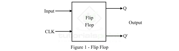
A flip-flop has one or more inputs and two outputs, usually represented by Q and Q' along with a clock input. The clock input is used to trigger the flip-flop so that it can change states of its outputs.
There are several types of flip-flops such as SR flip-flop, JK flip-flop, D flip-flop, and T flip-flop. Each type of flip-flop has its unique properties and characteristics needed for a particular purpose.
Synchronous and Asynchronous Flip-flops
A flip-flop whose logic circuit is clocked/triggered by a clock signal is known as a synchronous flip-flop. Thus, the output states of the synchronous flip-flop do not change in the absence of the clock signal, even if its inputs change many times.
On the other hand, an asynchronous flip-flop is one in which there is no clock signal, hence its output changes instantly on the application of inputs.
Now, let us discuss the clocked or synchronous S-R flip-flop in detail.
What is a Clocked SR Flip-flop?
The type flip-flop which has two inputs namely S (Set) and R (Reset) is termed as an SR flipflop. If the S and R inputs of the flip-flop control its outputs when a clock pulse is present (i.e. goes from either low to high or high to low), then it called a clocked SR flip-flop. Since, the clock signal synchronizes the operation of the SR flip-flop, hence the clocked SR flip-flop is also known as synchronous SR flip-flop. The block diagram of a clocked or synchronous SR flip-flop is shown in Figure-2.

The logic circuit diagram of the clocked or synchronous SR flip-flop is shown in Figure-3 below.
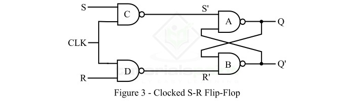
As it can be seen that the circuit consists of four NAND gates. The clock signal is connected to the NAND gates C and D and the inputs S and R also applied to the NAND gates C and D. The NAND gates A and B are cross-coupled to form the storage circuit of the flip-flop.
Operation of Clocked SR Flip-Flop
The operation of this circuit of clocked SR flip-flop is as described as follows −
- When the clock signal is not applied, the SR flip-flop circuit remains inactive, and there is no change in the outputs of the flip-flop.
- When the clock signal is applied, the flip-flop circuit becomes active and operates as explained below −
- When S = 0 and R = 0, the output of NAND gates C and D are S' = 1 and R' = 1. Hence, the outputs of the NAND gates A and B remains unchanged. This is called Hold State of the SR flip-flop.
- When S = 0 and R = 1, the output of the NAND gates C and D are S' = 1 and R' = 0, the output of the NAND gate A is 0 and that of NAND gate B is 1. This is called Reset State of the SR flip-flop.
- When S = 1 and R = 0, the output of the NAND gates C and D are S' = 0 and R' = 1, the output of the NAND gate A is 1 and that of the NAND gate B is 0. This is called Set State of the SR flip-flop.
- When S = 1 and R = 1, the output of the NAND gates C and D are S' = 0 and R' = 0, the outputs of the both NAND gates A and B try to become 1, which is not possible. This is called Forbidden State of the SR flip-flop.
Truth Table of Clocked SR Flip-Flop
We can also express the operation of the clocked SR flip-flop in the form of a truth table as given below. Here, S and R specifies the inputs, Qn specifies the present state of the output, and Qn+1 specifies the state of the output after change in input and application of clock pulse.
| Inputs | Output | Comment | ||
|---|---|---|---|---|
| S | R | Qn | Qn+1 | |
| 0 | 0 | 0 | 0 | No Change / Hold |
| 0 | 0 | 1 | 1 | No Change / Hold |
| 0 | 1 | 0 | 0 | Reset |
| 0 | 1 | 1 | 0 | Reset |
| 1 | 0 | 0 | 1 | Set |
| 1 | 0 | 1 | 1 | Set |
| 1 | 1 | 0 | X | Forbidden |
| 1 | 1 | 1 | X | Forbidden |
From this truth table of the clocked SR flip-flop we can directly write the Boolean expression for its output Qn+1 as follows −

Hence, the characteristics equation of the SR flip-flop is,
$$\mathrm{Q_{n+1}\:=\:S\:+\:R'Q_{n}}$$
Applications of Clocked SR Flip-Flop
The clocked SR flip-flops are used in the following applications −
- Digital counters
- Storage and shift registers
- Data storage elements
- Data transfer systems
- Frequency divider circuits, etc.
Conclusion
A clocked SR flip-flop is a sequential logic circuit used as a 1 bit storage device in digital systems. It has two inputs S (Set) and R (Reset). When R is high, SR flip-flop is said to be in reset state; when S is high, SR flip-flop is called in set state; when both inputs S and R are high, SR flip-flop is said to be in forbidden or invalid state; and when both inputs S and R are low, SR flip-flop is said to be in no change or hold state.
