- Digital Electronics - Home
- Digital Electronics Basics
- Types of Digital Systems
- Types of Signals
- Logic Levels And Pulse Waveforms
- Digital System Components
- Digital Logic Operations
- Digital Systems Advantages
- Number Systems
- Number Systems
- Binary Numbers Representation
- Binary Arithmetic
- Signed Binary Arithmetic
- Octal Arithmetic
- Hexadecimal Arithmetic
- Complement Arithmetic
- Base Conversions
- Base Conversions
- Binary to Decimal Conversion
- Decimal to Binary Conversion
- Binary to Octal Conversion
- Octal to Binary Conversion
- Octal to Decimal Conversion
- Decimal to Octal Conversion
- Hexadecimal to Binary Conversion
- Binary to Hexadecimal Conversion
- Hexadecimal to Decimal Conversion
- Decimal to Hexadecimal Conversion
- Octal to Hexadecimal Conversion
- Hexadecimal to Octal Conversion
- Binary Codes
- Binary Codes
- 8421 BCD Code
- Excess-3 Code
- Gray Code
- ASCII Codes
- EBCDIC Code
- Code Conversion
- Error Detection & Correction Codes
- Logic Gates
- Logic Gates
- AND Gate
- OR Gate
- NOT Gate
- Universal Gates
- XOR Gate
- XNOR Gate
- CMOS Logic Gate
- OR Gate Using Diode Resistor Logic
- AND Gate vs OR Gate
- Two Level Logic Realization
- Threshold Logic
- Boolean Algebra
- Boolean Algebra
- Laws of Boolean Algebra
- Boolean Functions
- DeMorgan's Theorem
- SOP and POS Form
- POS to Standard POS Form
- Minimization Techniques
- K-Map Minimization
- Three Variable K-Map
- Four Variable K-Map
- Five Variable K-Map
- Six Variable K-Map
- Don't Care Condition
- Quine-McCluskey Method
- Min Terms and Max Terms
- Canonical and Standard Form
- Max Term Representation
- Simplification using Boolean Algebra
- Combinational Logic Circuits
- Digital Combinational Circuits
- Digital Arithmetic Circuits
- Multiplexers
- Multiplexer Design Procedure
- Mux Universal Gate
- 2-Variable Function Using 4:1 Mux
- 3-Variable Function Using 8:1 Mux
- Demultiplexers
- Mux vs Demux
- Parity Bit Generator and Checker
- Comparators
- Encoders
- Keyboard Encoders
- Priority Encoders
- Decoders
- Arithmetic Logic Unit
- 7-Segment LED Display
- Code Converters
- Code Converters
- Binary to Decimal Converter
- Decimal to BCD Converter
- BCD to Decimal Converter
- Binary to Gray Code Converter
- Gray Code to Binary Converter
- BCD to Excess-3 Converter
- Excess-3 to BCD Converter
- Adders
- Half Adders
- Full Adders
- Serial Adders
- Parallel Adders
- Full Adder using Half Adder
- Half Adder vs Full Adder
- Full Adder with NAND Gates
- Half Adder with NAND Gates
- Binary Adder-Subtractor
- Subtractors
- Half Subtractors
- Full Subtractors
- Parallel Subtractors
- Full Subtractor using 2 Half Subtractors
- Half Subtractor using NAND Gates
- Sequential Logic Circuits
- Digital Sequential Circuits
- Clock Signal and Triggering
- Latches
- Shift Registers
- Shift Register Applications
- Binary Registers
- Bidirectional Shift Register
- Counters
- Binary Counters
- Non-binary Counter
- Design of Synchronous Counter
- Synchronous vs Asynchronous Counter
- Finite State Machines
- Algorithmic State Machines
- Flip Flops
- Flip-Flops
- Conversion of Flip-Flops
- D Flip-Flops
- JK Flip-Flops
- T Flip-Flops
- SR Flip-Flops
- Clocked SR Flip-Flop
- Unclocked SR Flip-Flop
- Clocked JK Flip-Flop
- JK to T Flip-Flop
- SR to JK Flip-Flop
- Triggering Methods:Flip-Flop
- Edge-Triggered Flip-Flop
- Master-Slave JK Flip-Flop
- Race-around Condition
- A/D and D/A Converters
- Analog-to-Digital Converter
- Digital-to-Analog Converter
- DAC and ADC ICs
- Realization of Logic Gates
- NOT Gate from NAND Gate
- OR Gate from NAND Gate
- AND Gate from NAND Gate
- NOR Gate from NAND Gate
- XOR Gate from NAND Gate
- XNOR Gate from NAND Gate
- NOT Gate from NOR Gate
- OR Gate from NOR Gate
- AND Gate from NOR Gate
- NAND Gate from NOR Gate
- XOR Gate from NOR Gate
- XNOR Gate from NOR Gate
- NAND/NOR Gate using CMOS
- Full Subtractor using NAND Gate
- AND Gate Using 2:1 MUX
- OR Gate Using 2:1 MUX
- NOT Gate Using 2:1 MUX
- Memory Devices
- Memory Devices
- RAM and ROM
- Cache Memory Design
- Programmable Logic Devices
- Programmable Logic Devices
- Programmable Logic Array
- Programmable Array Logic
- Field Programmable Gate Arrays
- Digital Electronics Families
- Digital Electronics Families
- CPU Architecture
- CPU Architecture
Edge-Triggered Flip-Flop
What is a Flip Flop?
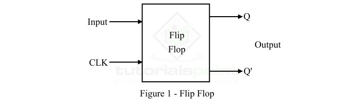
In digital electronics, a flip-flop (FF) is a sequential logic circuit which is used for storing 1-bit of information. As we know, in digital systems, information is represented in binary form, i.e. in terms of 0 and 1. Where, a binary 0 and a binary 1 is referred to as a bit.
The flip flop is a 1-bit memory cell that stores information in terms of 0 or 1. Therefore, flip flop is the fundamental memory element in all digital systems.
A flip flop has one or more inputs and two outputs. Where, one is the normal output denoted by Q and the other is inverted output denoted by Q'. Hence, a flip flop has two stable states due to which it is also known as bistable multivibrator.
The logic symbol diagram of a typical flip-flop is shown in Figure-1.
Based on the response to the clock pulse, flip flops are of two types namely, level-triggered flip flop and edge-triggered flip flop.
The type of flip flop whose operation is controlled by a continuous clock signal and its output state changes when the clock pulse is in a particular level either high or low is known as a level-triggered flip flop. On the other hand, the type of flip flop which respond when the clock change its state, i.e. either goes from high to low or low to high is known as an edgetriggered flip flop. We will discuss the edge-triggered flip flop in more detail in this article.
What is an Edge-Triggered Flip-Flop?
The type of digital circuit which is capable of storing 1-bit of information and responds only when a specific edge of the clock pulse occurs is known as an edge-triggered flip-flop.
Therefore, the output state of the edge-triggered flip flop updates only when a specific edge of the clock pulse occurs, i.e. the clock pulse goes from either low to high or high to low states. This flip flop does not respond to a continuous clock pulse.
Edge-triggered flip-flop are used in several digital circuits where the output of the flip flop should be updated when the clock pulse changes its state from 0 to 1 or 1 to 0 as shown in Figure-2.
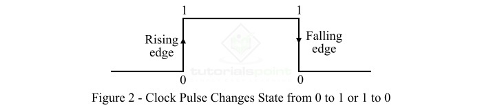
Hence, the edge triggered flip flop operates only on the rising or falling edge of the clock pulse.
Types of Edge-Triggered Flip-Flop
Depending on the responding edge of the clock pulse, the edge-triggered flip flops are classified into two types namely,
- Positive Edge-Triggered Flip-Flop
- Negative Edge-Triggered Flip-Flop
Positive Edge-Triggered Flip-Flop
The type of edge-triggered flip-flop whose output changes its state only on the rising edge (edge that goes from low to high) of the clock pulse is called a positive edge-triggered flip-flop. The positive edge triggered flip flop is also called a rising edge-triggered flip-flop. The block diagram of a positive edge triggered flip flop is shown in Figure-3 below.
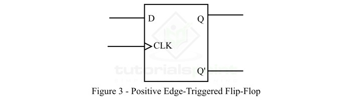
In a positive edge triggered flip flop, the inputs are accepted and stored only when the clock pulse goes from low (0) to high (1), i.e. on the rising edge of the clock pulse. This stored value is then available on the outputs.
Negative Edge-Triggered Flip-Flop
The type of edge-triggered flip flop whose output changes its state only on the falling edge (edge that goes from high to low) of the clock pulse is called a negative edge-triggered flip-flop. The negative edge triggered flip flop is also known as a falling edge-triggered flip-flop. The block diagram of a negative edge triggered flip flop is shown in Figure-4 below.
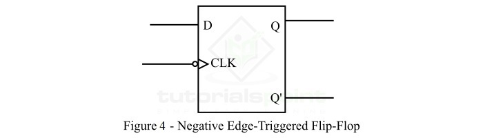
In the case of negative edge triggered flip flop, the flip-flop captures and stores the inputs only when the clock pulse goes from high to low, i.e. on falling edge of the clock pulse.
Operation of Edge-Triggered Flip-Flop
The operation of a typical edge-triggered flip-flop is described below
In the edge-triggered flip-flop, the inputs are applied through the input terminals and a clock pulse is connected to the clock input of the flip-flop. The edge triggered flip flop responds according to the applied inputs when the clock pulse goes from either low to high or high to low. When this state transition of clock pulse occurs, the flip-flop captures and stores the input values. These stored input values will be then available on the outputs (Q and Q') of the flip-flop.
Advantages of Edge-Triggered Flip-Flop
The important advantages of the edge-triggered flip flop are listed as follows
- Edge triggered flip flops have an improved timing behavior as compared to the level triggered flip flops. This is because, the edge triggered flip flop responds only on the transition of clock pulse.
- Edge-triggered flip flops reduces the possibility of glitches that cause errors in the system.
- Edge triggered flip flops consumes relative low power than the level-triggered flip flops.
- Edge-triggered flip flop has relatively less complex circuit design.
- Edge triggered flip flops can be easily integrated in the form of digital ICs.
- Edge triggered flip flops are very useful in digital systems having very high clock speed.
Applications of Edge-Triggered Flip-Flop
Edge triggered flip flops are used in a variety of digital systems. Some common applications of edge triggered flip flops are −
- Edge triggered flip-flops are used in registers to store and transfer binary information among different parts of a digital circuit.
- Edge triggered flip flops are used in digital counters for generating sequences of binary values.
- Edge triggered flip flops are also used for digital signal processing.
- Edge triggered flip flops are used in several digital applications where timing and signal synchronization is required.
- Edge-triggered flip flops are also used to build memory cells of ROM, RAM, etc. to stores binary data in a digital system.
This is all about edge triggered flip-flop. In conclusion, edge triggered flip-flops are one of the important building blocks of many digital systems such as memories, registers, counters, etc.
