- Digital Electronics - Home
- Digital Electronics Basics
- Types of Digital Systems
- Types of Signals
- Logic Levels And Pulse Waveforms
- Digital System Components
- Digital Logic Operations
- Digital Systems Advantages
- Number Systems
- Number Systems
- Binary Numbers Representation
- Binary Arithmetic
- Signed Binary Arithmetic
- Octal Arithmetic
- Hexadecimal Arithmetic
- Complement Arithmetic
- Base Conversions
- Base Conversions
- Binary to Decimal Conversion
- Decimal to Binary Conversion
- Binary to Octal Conversion
- Octal to Binary Conversion
- Octal to Decimal Conversion
- Decimal to Octal Conversion
- Hexadecimal to Binary Conversion
- Binary to Hexadecimal Conversion
- Hexadecimal to Decimal Conversion
- Decimal to Hexadecimal Conversion
- Octal to Hexadecimal Conversion
- Hexadecimal to Octal Conversion
- Binary Codes
- Binary Codes
- 8421 BCD Code
- Excess-3 Code
- Gray Code
- ASCII Codes
- EBCDIC Code
- Code Conversion
- Error Detection & Correction Codes
- Logic Gates
- Logic Gates
- AND Gate
- OR Gate
- NOT Gate
- Universal Gates
- XOR Gate
- XNOR Gate
- CMOS Logic Gate
- OR Gate Using Diode Resistor Logic
- AND Gate vs OR Gate
- Two Level Logic Realization
- Threshold Logic
- Boolean Algebra
- Boolean Algebra
- Laws of Boolean Algebra
- Boolean Functions
- DeMorgan's Theorem
- SOP and POS Form
- POS to Standard POS Form
- Minimization Techniques
- K-Map Minimization
- Three Variable K-Map
- Four Variable K-Map
- Five Variable K-Map
- Six Variable K-Map
- Don't Care Condition
- Quine-McCluskey Method
- Min Terms and Max Terms
- Canonical and Standard Form
- Max Term Representation
- Simplification using Boolean Algebra
- Combinational Logic Circuits
- Digital Combinational Circuits
- Digital Arithmetic Circuits
- Multiplexers
- Multiplexer Design Procedure
- Mux Universal Gate
- 2-Variable Function Using 4:1 Mux
- 3-Variable Function Using 8:1 Mux
- Demultiplexers
- Mux vs Demux
- Parity Bit Generator and Checker
- Comparators
- Encoders
- Keyboard Encoders
- Priority Encoders
- Decoders
- Arithmetic Logic Unit
- 7-Segment LED Display
- Code Converters
- Code Converters
- Binary to Decimal Converter
- Decimal to BCD Converter
- BCD to Decimal Converter
- Binary to Gray Code Converter
- Gray Code to Binary Converter
- BCD to Excess-3 Converter
- Excess-3 to BCD Converter
- Adders
- Half Adders
- Full Adders
- Serial Adders
- Parallel Adders
- Full Adder using Half Adder
- Half Adder vs Full Adder
- Full Adder with NAND Gates
- Half Adder with NAND Gates
- Binary Adder-Subtractor
- Subtractors
- Half Subtractors
- Full Subtractors
- Parallel Subtractors
- Full Subtractor using 2 Half Subtractors
- Half Subtractor using NAND Gates
- Sequential Logic Circuits
- Digital Sequential Circuits
- Clock Signal and Triggering
- Latches
- Shift Registers
- Shift Register Applications
- Binary Registers
- Bidirectional Shift Register
- Counters
- Binary Counters
- Non-binary Counter
- Design of Synchronous Counter
- Synchronous vs Asynchronous Counter
- Finite State Machines
- Algorithmic State Machines
- Flip Flops
- Flip-Flops
- Conversion of Flip-Flops
- D Flip-Flops
- JK Flip-Flops
- T Flip-Flops
- SR Flip-Flops
- Clocked SR Flip-Flop
- Unclocked SR Flip-Flop
- Clocked JK Flip-Flop
- JK to T Flip-Flop
- SR to JK Flip-Flop
- Triggering Methods:Flip-Flop
- Edge-Triggered Flip-Flop
- Master-Slave JK Flip-Flop
- Race-around Condition
- A/D and D/A Converters
- Analog-to-Digital Converter
- Digital-to-Analog Converter
- DAC and ADC ICs
- Realization of Logic Gates
- NOT Gate from NAND Gate
- OR Gate from NAND Gate
- AND Gate from NAND Gate
- NOR Gate from NAND Gate
- XOR Gate from NAND Gate
- XNOR Gate from NAND Gate
- NOT Gate from NOR Gate
- OR Gate from NOR Gate
- AND Gate from NOR Gate
- NAND Gate from NOR Gate
- XOR Gate from NOR Gate
- XNOR Gate from NOR Gate
- NAND/NOR Gate using CMOS
- Full Subtractor using NAND Gate
- AND Gate Using 2:1 MUX
- OR Gate Using 2:1 MUX
- NOT Gate Using 2:1 MUX
- Memory Devices
- Memory Devices
- RAM and ROM
- Cache Memory Design
- Programmable Logic Devices
- Programmable Logic Devices
- Programmable Logic Array
- Programmable Array Logic
- Field Programmable Gate Arrays
- Digital Electronics Families
- Digital Electronics Families
- CPU Architecture
- CPU Architecture
Digital Electronics - Quick Guide
Types of Digital Systems
A system is defined as a group of various components interconnected together to perform a specific task. For example, a digital computer consists of several components such as monitor, CPU (Central Processing Unit), memory, keyboard, mouse, printer, and more. All these components are connected together to accomplish certain tasks. Hence, a computer can be termed as a system.
We can broadly classify systems into the following two categories −
- Analog Systems
- Digital Systems
An analog system is a type of system that operates on continuous time signals, while a digital system is one that can work on discrete time signals.
Read this chapter to learn the basics of digital systems and their types.
What is a Digital System?
A type of electronic system that is designed to store, manipulate, and communicate digitally represented information is termed as a digital system. Some common examples of digital systems include smartphone, laptops, smartwatch, tablet, desktop computers, etc.

The working of a digital system is entirely based on digital signals or binary signals. Where, a digital signal is a type of signal that is represented as a discrete-elements. It can have two possible states namely high or low. The high state is denoted by the logic 1 and the low state is denoted by the logic 0.
In a digital system, if the state of the signal is logic 1, the system will be on, and if the state of the signal is 0, the system will be off.
Characteristics of Digital Systems
Today, digital systems are widely used in almost every aspect of life. This is because of their high reliability and efficiency. The following are some key characteristics of digital systems −
- Digital systems are relative less complex to implement as they use binary number system having only two digits to represent the state of a system.
- In digital systems, the information is represented in the form of a group of 0s and 1s i.e., bits. This is called binary or digital representation of information.
- Digital systems rely on digital signals having two well-defined discrete states. This makes digital systems more reliable and efficient in terms of processing, storage, and communication of information.
- Digital systems use logical mathematics and operations to perform computing tasks.
- Digital systems can be manufactured in the form of integrated circuits (ICs) of very small sizes.
- Digital systems can be easily programmed to perform repeated tasks that reduces human efforts and cost.
- Digital systems are highly immune to noise and distortions.
Types of Digital Systems
Digital systems can be classified based on various parameters. Here are some important types of digital systems that we commonly use in practice −
Combinational Digital Systems
A combinational logic circuit or system is a type of digital circuit that performs logical operations and produces output depending on the present inputs. Hence, the output of a combinational digital circuit does not depend on the past inputs and outputs of the system.
Example − The common examples of combinational digital systems are binary adders, subtractors, logic gates, multiplexers, demultiplexers, etc.
Sequential Digital Systems
A type of digital system that has a memory element to store past history of the system operation is called a sequential digital system. Therefore, the output of a digital system depends on both present inputs and past outputs of the system.
Example of sequential digital systems are flip-flops, registers, memory devices, counters, etc.
Programmable Logic Devices (PLDs)
A programmable logic device is one that can be programmed to perform a specific task automatically.
Example of programmable logic devices are microcontrollers, PLCs, etc.
Digital Communication Systems
A digital communication system is a type of digital system used for transmission and reception of information in the form of digital signals.
Example of digital communication systems are internet, intranet, mobile communication system, Wi-Fi, etc.
Digital Control Systems
A digital control system is a computerized control system used to monitor and regulate the behavior of a dynamic system.
Example − Digital control systems are extensively used in robotics, industrial automation, etc.
Conclusion
In conclusion, digital systems are modern systems known for their high speed and reliability. A digital system utilizes digital signals to store, process, and communicate the information.
In this chapter, we explained the basics of digital systems and their types. Traverse to the next chapter to learn all about the types of signals used in the field of electronics engineering.
Types of Signals
In electronics engineering, an electrical quantity like voltage or current or electromagnetic wave that is used for transmission of data or information is called a signal.
Signals are considered the heart of any data communication or processing system like the Internet. Signals instruct the electronics hardware components to perform a certain task such as convey the information from one point to another.
Apart from voltage, current or electromagnetic signals, we also have optical signals, where the information is represented and transmitted in the form of light.
This chapter will explain the concept of signal and different types of signals used in electronics engineering.
What is a Signal?
A physical quantity that has capability to transmit information from one point to another is called a signal. Some common examples of signals include voltage, current, electromagnetic wave, optical signals, etc.
Signals are the backbone of any electronic processing or communication system. These can be transmitted through various types of communication channels like wires, space (electromagnetic waves), optical fibers, etc.
Properties of Signal
In electronics, a signal is characterized by the following important properties −
- Magnitude − The intensity or maximum value of a signal is termed as its magnitude.
- Frequency − The number of oscillations per second is called frequency of the signal.
- Time period − The time taken to complete one oscillation is called the time period of the signal.
Types of Signals
In electronics, there are mainly two types of signals used, they are −
- Analog Signals
- Digital Signals
Let us discuss these two types of signals in detail.
What is an Analog Signal?
A type of electronic signal that has continuous values within a given range is called an analog signal. Analog signals are expressed as the continuous functions of time. They are represented as the waveforms of continuously varying current or voltage.
Example of analog signals are voice, speed, pressure, temperature, etc.

An important characteristic of analog signals is that they have a definite value at every instant of time, known as instantaneous value of the signal.
Analog signals have smooth waveforms as they are continuous in both amplitude and time. That meant, there is no interruptions in their representation over time.
Properties of Analog Signal
The following are main properties of analog signals −
- Analog signals are continuous signals in both amplitude and time.
- Analog signals have a certain value or magnitude at any given instant of time.
- Analog signals have infinite resolution.
- Analog signals are best suited for representing the real-world phenomena.
- Analog signals are represented by the continuously varying smooth waveforms.
What is a Digital Signal?
A digital signal is a type of electronic signal that has a finite set of discrete values representing information.

Digital signals are also called binary signals, as they use binary 0 or 1 to represent the state of a signal. Where, the binary 0 represents the off or low state of the signal, while the binary 1 represents the on or high state of the signal.
Thus, digital signals are expressed as discontinuous functions of time.
Properties of Digital Signal
The following are some key characteristics of digital signals −
- Digital signals have discrete or discontinuous values in terms of both amplitude and time.
- Digital signals do not have values defined between any two distinct instants of time.
- Digital signals are represented using binary system by sampling the values of the signals at specific time instants.
- Digital signals represent information in the form of a sequence of binary 0s and 1s.
- Digital signals have a finite resolution.
- Digital signals are capable to perform logical operations.
- Digital signals are more efficient and reliable when it comes to storage and transmission.
Difference between Analog and Digital Signals
Let us now discuss the important differences between analog and digital signals −
| Key | Analog Signals | Digital Signals |
|---|---|---|
| Representation | Analog signals are represented as continuous functions or waveforms of time. | Digital signals are represented as discrete functions of time. |
| Nature | Analog signals are continuous as they have infinite values within a specified range. | Digital signals are discontinuous as they have distinct values sampled at specific time instants. |
| Resolution | Analog signals have infinite resolution. | Digital signals have a finite resolution. |
| Accuracy | Analog signals are more accurate. | Digital signals are relatively less accurate. |
| Storage | Analog signals are difficult to store. | Digital signals are efficient to store. |
| Noise immunity | Analog signals are less immune to noise. | Digital signals have high immunity against noise. |
| Examples | Voice signals, temperature, speed, etc. | Data transmitted over internet, computer generated signals, etc. |
Applications of Signals
Both analog and digital signals are widely used in the field of electronics. The following are some key applications of signals −
- Signals are used for storage and transmission of information.
- Signals are used in control systems to regulate their behavior.
- Signals are also used in measurement of physical quantities like temperature, pressure, speed, sound, light, and more.
- Signals are used in computing systems for data processing, etc.
Conclusion
In electronics engineering, signals are most significant elements of a system. Signals are nothing but physical quantities like voltage, current, electromagnetic waves, light pulses, etc. used to convey information from one point to another.
In this chapter, we covered different types of signals and their properties. In the next chapter, we will cover the concept of logic levels and pulse waveform.
Logic Levels and Pulse Waveforms
A digital system is a type of electronic system that utilizes the binary number system to work. In other words, a digital system is a two-state electronic system used to represent two binary digits 0 and 1, where 0 represents the low or "off" state and 1 represents the high or "on" state of the system.
In the field of digital electronics, different voltage levels are used to represent the two binary values, i.e., 0 and 1 in a digital signal. These voltage levels are known as logic levels.
In this chapter, we will learn the concept of logic levels and pulse waveforms.
What is a Logic Level?
In digital electronics, a voltage level that represents a specific binary value either 0 or 1 is called a logic level. Here, the binary value 0 represents the low voltage level while the binary value 1 represents the high value level.
Hence, the logic levels can be classified into the following two types −
- High Logic Level
- Low Logic Level
Lets discuss these two logic levels in detail.
High Logic Level
In the case of a digital system, the voltage level closer to the maximum voltage level that the system can handle without getting damaged is called high logic level.
The high logic level is represented by the binary digit "1". The voltage level for a high logic level depends on the technological standard used to design the system. Typically, the voltage value between 2 V and 5 V represents the high logic level or 1.
Low Logic Level
In a digital system, the low logic level is defined as the maximum voltage level for which the system will remain in the OFF state.
The low logic level is represented by the binary digit "0". Similar to the high logic level, the voltage level for a low logic level depends on the technology standard used to design the system. In actual practice, the voltage value between 0 V and 0.8 V represents the low logic level or logic 0.
In most practical digital system, the ground voltage is used to represent the low logic level.
Note − The voltage range between the voltage values 0.8 V and 2 V is known as the indeterminate logic range. If a digital signal lies between the value 0.8 and 2 V, the response of the system is not predictable.
What is a Pulse?
A pulse is a type of an electronic signal that can change suddenly between two possible states i.e., high state and low state.
The graph used to represent the transition of a pulse is called the pulse waveform. Pulses are very important in the operation of digital systems, communication systems, and many other electronics devices and circuits.
Depending on the switching characteristics, the pulses can be classified into the following two types −
- Positive Pulse − When a signal normally goes from low logic level to the high logic level and then returns to its normal low logic level, then it is called a positive pulse.
- Negative Pulse − When a signal normally goes from high logic level to the low logic level and then returns to its normal high logic level, then it is known as a negative pulse.
The pulse waveforms for positive and negative pulses are depicted in the following figure.

A pulse has two edges namely, a leading edge and a trailing edge.
In the case of a positive pulse, the edge going from low logic level to high logic level is called the leading edge, and the edge going from high logic level to low logic level is called the trailing edge.
In the case of a negative pulse, the edge going from high logic level to low logic level is called the leading edge, whereas the edge going from low logic level to high logic level is called the trailing edge.
The positive and negative pulse waveforms shown in the above figure are ideal pulse waveforms, because their leading and trailing edges change instantaneously i.e., in zero time. But in actual practice, the edges of pulses do not change instantaneously from low logic level to high logic level or from high logic level to low logic level.
The pulse waveforms that take a finite time to change from low logic level to high logic level and vice-versa are known as non-ideal pulse waveforms.

In the case of a non-ideal pulse waveform, the time taken by the pulse to go from low logic level to high logic level is called the rise time. The time taken by the pulse to go from the high logic level to the low logic level is called the fall time.
Types of Pulse Waveforms
The pulse waveforms used in digital systems are mainly classified into the following two types −
Periodic Waveforms
A pulse waveform that repeats itself at regular intervals of time is called a periodic waveform. The time taken to complete one cycle is called the time period of the periodic waveform.
Non-periodic Waveforms
A pulse waveform which does not repeat itself at regular intervals of time is termed as a non-periodic or aperiodic waveform.
Conclusion
In conclusion, "logic level" is a concept used in digital systems to represent the state of the system. There are two possible logic levels in the case of digital systems namely, high logic level and low logic level. The high logic level is represented by the binary 1 while the low logic level is represented by the binary 0.
The graphical representation of a digital signal or a pulse is termed as the "pulse waveform". Pulse waveforms are used to represent the transition of a pulse or digital signal or the states of a digital system. In this chapter, we have discussed the concept of logic levels and pulse waveforms. In the next chapter, we will learn about "components of a digital system".
Components of Digital System
A digital system is a type of electronic system used to store, process, and manipulate data represented in the form of digital signals, where a digital signal is a discrete time signal. Digital systems use binary number system to operate. Some common examples of digital systems include digital computers, laptops, smartphones, etc.
This chapter is meant for explaining the major components of a digital system.

Components of a Digital System
A typical digital system consists of the following main components −
- Central Processing Unit (CPU)
- Memory
- Input Devices
- Output Devices
- Logic Gates
- Power Supply
- Communication Channels
Lets discuss each of these components of a digital system in detail.
Central Processing Unit (CPU)
In a digital system, the central processing unit is the most important component of the system, as it performs all the operations in the system. It is also known as processor.
The CPU is an electronic circuit that consists of two sub-circuits namely, arithmetic and logic unit, and control unit.
The arithmetic logic unit (ALU) is the part of a CPU that performs all the arithmetic and logical operations and executes the instructions to manipulate data. ALU is made up of logic gates and other electronic components. It can perform operations like addition, subtractions, comparison, etc.
The control unit (CU) is another major electronic circuit in the central processing unit that coordinate the operation of all other components of a digital system. It generates clock signals for the synchronization of the system.
Semiconductor Memory
Memory is another major component of a digital system. It is used to store and instructions in the system. In most digital system, semiconductor memory is used to store digital information.
Memory of a digital system can be classified into the following two types −
- Random Access Memory (RAM) − It is a temporary memory used to store data and instruction on which the CPU is currently working. Once the digital system is turned off, its data will be deleted.
- Read Only Memory (ROM) − ROM is also an important component of a digital system. It is a permanent memory used to store those data and instructions that require again and again to perform tasks.
In digital systems, both RAM and ROM are used in the form of ICs made up of semiconductors.
Apart from RAM and ROM, digital systems may also support external memory devices like CD, DVD, Pen Drive, SD card, etc. All these external memories are used for permanent data storage.
Input Devices
Input devices are those electronic components of a digital system used for entering data into the system. Examples of input devices include keyboard, mouse, scanner, sensors, camera, light pen, code readers, etc.
Input devices are designed to accept data in the form of a specific type or format and convert them into digital signals for processing.
For example, a keyboard gets outside instructions in the form of keystrokes and then convert them into digital signals.
Output Devices
Output devices are those components of a digital system that allow users to view the processed data or information. Examples of output devices are monitor, display screens, printers, projectors, speakers, etc.
Output devices are designed to accept digital signals and convert them in a suitable format to make them readable by human.
For example, a monitor takes digital signals and convert them as visuals and display on a screen.
Logic Gates
Logic gates are essential components of any digital system. They are the fundamental building block of the digital system. Logic gates are nothing but electronic circuits that can perform logical operations.
In digital systems, logic gates are used to realize all the information processing and storage systems. The most commonly used logic gates are AND, OR, NOT, NAND, NOR, Ex-OR, and Ex-NOR.
Power Supply
Power supply is the energy bank of the digital system that provides necessary electric power to the components of the system so they can work.
The primary function of the power supply unit of a digital system is to convert the electric power received from an external source into the desired type and voltage level required by the system.
Most digital systems work on 5 V DC supply. Hence, the power supply unit receives 220 V AC from the supply mains and convert it to 5 V DC supply. Also, the power supply unit regulates the fluctuations occurring in the power supply to protect the system from damages.
Communication Channels
In a digital system, the communication channel is also known as bus system. It consists of several different types of buses (conductors) such as data bus, address bus, and control bus. These communication channels allow data transmission between different components of the system.
Conclusion
In conclusion, a digital system consists of several components. Some important components of a typical digital system are described in this chapter. All these components are connected together and allowed to communicate to perform different jobs. In the next chapter, we will learn about different types of "digital logic operations".
Digital Logic Operations
In the field of digital electronics, many digital logic operations are performed which are considered as the fundamental building blocks. All the digital logic operations are based on the binary number system and Boolean algebra, where the data and information are represented in the form of binary 0s and 1s. Digital logic operations are used to manipulate the binary digits to perform various tasks.
In this chapter, we will learn about commonly used digital logic operations in the field of digital electronics. Here are some widely used digital logic operations −
- Arithmetic Operations
- Logical Operations
- Encoding and Decoding
- Multiplexing and Demultiplexing
- Code Conversion
- Comparison
- Counting
- Data Storage
- Data Transmission
Lets discuss each of these digital logic operations in detail along with their applications.
Arithmetic Operations in Digital Electronics
Arithmetic operations are basic mathematical operations like addition, subtraction, multiplication, division, etc. In digital electronics, these arithmetic operations are performed using various digital circuits like adders, subtractors, multiplier, etc.
In digital electronic systems, the given numbers are first converted into binary format and then desired operations are performed on them.
Arithmetic operations are one of the fundamental operations performed using various digital electronic systems like microprocessors, calculators, microcontrollers, etc.
The following are the four main arithmetic operations performed by a digital system −
Addition
Addition is performed by using a digital logic circuit called adder. It adds two numbers and generates a sum and a carry as output. For example, if 8 and 5 are two numbers, then adder will produce a sum term 3 and a carry output 1.
Subtraction
The arithmetic operation subtraction is performed by using a digital logic circuit called subtractor. It performs the subtraction of two numbers and produces a difference term and a borrow term as output.
Multiplication
A digital circuit used to perform multiplication of two numbers is called a multiplier. It multiplies the given numbers and generates a product term as output.
Division
The division operation of two numbers is performed by using a digital circuit called divider. It performs division of two numbers and generates a quotient term and remainder term as output.
Logical Operations in Digital Electronics
Logical operations are used to compare two input parameters to make a decision. The commonly used logical operations in digital systems are OR, AND, NOT, NAND, NOR, XOR, and XNOR. All these logical operations are used to manipulate binary data to make crucial decisions in a digital system.
Logical operations are widely used for developing algorithms and conditional statements in programming.
Here are the commonly used logical operations in digital electronics −
AND
It is a basic logic operation performed by using a digital circuit called AND gate. In the AND operation, the output is true only if all of the inputs are true.
OR
OR is another basic logic operation in digital electronics. It is performed by using a digital logic circuit called OR gate. It produces a true output if any of the inputs are true.
NOT
NOT is a digital logic operation performed by using a circuit called NOT gate or inverter. It is also known as inversion operation. It generates a complement of the input.
NAND
NAND is a combination of AND and NOT operation. It is performed by using a digital circuit called NAND gate. The output of the NAND gate is false only if all of the inputs are true.
NOR
This logical operation is a combination of OR and NOT operations. It is performed by using a digital circuit called NOR gate. In the case of NOR operation, the output is false if any of the inputs are true.
XOR
The logical operation XOR or Exclusive OR is performed by using a digital logic circuit called XOR gate. In the case of XOR operation, the output is true if the number of true inputs is odd.
XNOR
The logical operation XNOR is a combination of XOR and NOT operations. It is performed by using a digital logic circuit called XNOR gate. In the case of XNOR gate, the output is true if all of the inputs are either true or false.
Encoding and Decoding in Digital Electronics
In digital electronics, encoding is a digital logic operation used to convert a familiar number or symbol into a coded format. A digital circuit called encoder is used to perform encoding, where the encoder receives digits, alphabets, and symbols and converts them into their respective binary codes.
On the other hand, decoding is the inverse operation of encoding. It is performed by using a digital logic circuit called decoder. Decoding is a digital logic operation that involves the conversion of a binary-coded information to other format like decimal, octal, hexadecimal, alphabets or symbols.
Both encoding and decoding are used in digital communication, error correction, data compression, etc.
Multiplexing and Demultiplexing in Digital Electronics
Multiplexing is a digital logic operation that combines multiple signals into a single signal. Hence, it is also termed as data sharing or selecting. A digital circuit called multiplexer is used to perform multiplexing. Multiplexing involves the process of switching information from multiple input lines on to a single output line in a specific sequence.
Demultiplexing is the reverse process of multiplexing. In the case of demultiplexing, information is switched from one input line on to multiple output lines. The digital circuit used to perform demultiplexing is called a demultiplexer.
Multiplexing and demultiplexing are two widely used digital logic operation in optimization of communication channels.
Code Conversion in Digital Electronics
Code conversion is a digital logic operation that involves converting information coded in one form to another form. It is performed by using a digital circuit called code converter.
Code conversion is an essential operation in interfacing between different digital systems. Some common examples of code converters are BCD to XS-3 converter, XS-3 to gray converter, etc.
Comparison Operation in Digital Electronics
Comparison is a digital logic operation performed using a digital circuit called comparator. The comparator compares two quantities and generates an output signal indicating whether the two input quantities are equal or not.
Counting Operation in Digital Electronics
Counting is a digital logic operation performed by using a digital circuit called counter. It involves the counting of increase or decrease in binary numbers.
Counting operation plays a vital role in various digital devices like memory, timers, digital clocks, microprocessors, etc. It is used to control the sequence of operation in a digital system.
Data Storage in Digital Electronics
Data storage is an essential operation in digital systems. It involves storing and retrieving digital data and information stored in the memory devices. Data storage can be performed using various digital storage devices like flip-flops, registers, memory units, etc.
Data Transmission in Digital Electronics
Data transmission is a digital logic operation in which binary data is transferred from one point to another in a digital system. In digital electronics, data transmission can be done either through wires or wireless channels.
Data transmission is a fundamental operation in digital communication where data is exchanged between different components of the system.
Conclusion
In conclusion, digital logic operations are used to manipulate binary data to perform various operations. They are considered as the fundamental building blocks of digital systems like microprocessors, microcontrollers, memory devices, communication systems, etc. Hence, it is essential to understand the digital logic operations for designing reliable digital systems and understand their behavior.
In this chapter, we covered all the essential digital logic operations along with their applications. In the next chapter, we will learn the advantages and limitations of digital systems.
Advantages and Limitations of Digital Systems
A digital system is an interconnected group of components that can process, store, and transmit digital data i.e., data represented in the form of binary codes. Digital signals are represented using binary values, 0s and 1s. A digital system can understand and manipulate data and information represented in the form of 0s and 1s.
Digital systems are implemented using highly reliable and efficient electronics components like logic gates and integrated circuits (ICs). They are known for their high speed and reliability.
Digital systems are extensively used in various fields like communication, computing, control system, data processing, etc.
Examples of digital systems are computers, smartphones, tablets, telecommunication networks, etc. Today, digital systems form an essential part of our modern technological world. In this chapter, let's focus on the advantages and disadvantages of digital systems.
Advantages of Digital Systems
Digital systems offer several advantages over analog systems. Some of the important advantages of digital systems are explained below −
Easy to Design
As we know, digital systems are two state switching circuits that have only two voltage levels namely, HIGH and LOW. Hence, it is easier to design a digital system.
In the case of digital systems, the knowledge of intermediate values of voltages are not important, but the lower and upper limits in which they fall are important. Therefore, digital circuits are less complex to design and implement.
Easy Information Storage
In digital systems, data and information are represented in the form of binary digits, i.e., 0s and 1s. There are several types of magnetic, optical, and semiconductor memories available to store digital data.
It is very easy to store digital information in a digital storage device like pen drive that provides a compact and efficient method to store data for long periods as compared to analog storage devices.
High Accuracy and Precision
Digital systems have higher accuracy and precision as compared to analog systems. This is because, it is very easy to expand a digital system to handle more binary digits just by adding more digital circuits to the system.
Also, digital systems are highly immune to interference. Hence, they can process, store, and transmit data without loss of accuracy.
Flexibility in Programming and Versatility
The operation of a digital system can be controlled by writing a set of instructions called program. We can easily reprogram the system to change its operation without changing its hardware configuration. Hence, digital systems are more versatile than analog systems.
High Noise Immunity
In digital electronics, unwanted electronic signals are called noise. The electronic noise can disturb the normal operation of a system. Digital systems can have various error checking and correction mechanisms that make them more immune to noise and interference over analog systems.
High Reliability and Durability
Digital systems use components that are less susceptible to variations and aging. This characteristic makes the digital systems more reliable and durable as compared to analog systems. Hence, digital systems can be used with consistent performance for long periods.
Easy Fabrication on IC Chips
The fabrication of digital integrated circuits is simple and less costly as compared to analog ICs. Also, higher degree of integration can be achieved in the case of digital ICs, as the digital ICs do not require high value capacitors, precision resistors, and inductors.
High Security
Digital systems are highly secure than analog systems, as we can implement various advanced security and encryption technologies to protect sensitive information stored in the system.
All these are the major benefits of digital systems that make them suitable for various applications like computing, telecommunication, automation, robotics, and more.
However, digital systems also have certain limitations over analog systems. Lets discuss these limitations of digital systems in the following section.
Limitations of Digital Systems
Digital systems have numerous advantages, but they can also have some limitations that play a vital role in their designing and applications. The following are some key limitations of digital systems −
Need of Analog to Digital Conversion
In the real world, most physical quantities are analog in nature. Hence, before processing using a digital system, we need to convert these analog quantities into digital form. At the end of processing, the results are also converted back to the analog form.
Increased Complexity and Cost
As the digital systems require analog to digital and digital to analog converter and complex algorithms to perform operations. These practices increase complexity and cost of designing of the system.
Slow Processing Speed
Although digital systems have fast speeds, they cannot be used in some real-time applications due to need of extremely high processing speed. Under such situations, analog systems are more suitable over digital systems.
Sampling Rate Limitations
Real-world signals are analog, hence, proper sampling is important while converting them into digital signals. If the sampling rate is not chosen correctly, it can result in the loss of information in the digital system. Hence, digital systems are also subjected to a limitation in sampling rate.
Voltage Level Limitations
As digital systems use binary volage levels i.e., HIGH and LOW voltages. Therefore, they are limited in a certain range of voltage levels. Due to this reason, digital systems cannot be used in applications where a continuous range of voltages is required.
Conclusion
Digital systems have several advantages that make them suitable to use in modern technological applications. Due to high reliability, ease of integration, high security, etc. digital systems are being widely used in various fields like telecommunication, medical, science, research, etc.
Electronics engineers and designers are continuously working to optimize the digital systems to increase their performance and area of applications.
Digital systems however have some limitations like finite resolution, limited voltage levels and sampling rates, relatively slow speed, etc. These limitations have to be addressed while designing and implementation for better advancement in digital technologies.
Digital Electronics - Number Systems
A digital number system is a positional number system that has some symbols called digits. It provides a complete set of digits, operators, and rules to perform operations.
In a digital number system, the number of digits used determines the base of the number system. For example, the binary number system has two digits (0 and 1), hence, the base of the binary number system is 2.
Digital number systems form the foundation of the modern computing technologies and digital electronics. They are used to represent, process, and manipulate the information using a digital system.
In this chapter, we will discuss the fundamental concepts of different types of digital number systems.
Types of Digital Number Systems
In digital electronics, the following four types of digital number systems are mainly used −
- Binary Number System
- Decimal Number System
- Octal Number System
- Hexadecimal Number System
Lets discuss each of these number systems in detail.
Binary Number System
Binary number system is the fundamental building block behind the implementation and working of all digital systems.
Binary number system has two symbols or digits, i.e., 0 and 1. Hence, these two digits are used to represent information and perform all the digital operations. Each binary digit is called a bit.
Since there are two digits are used in the binary number system, hence its base is 2. Therefore, the value of a binary number is calculated as the sum of powers of 2.
Binary digits are used in digital system to represent their ON and OFF states. Where, 0 is used to represent the OFF state of the digital system and 1 is used to represent the ON state of the system.
Overall, the binary number system forms the foundation of computation, digital communication, and digital information storage.
Example
Consider the binary number 1101.011. The integer part of this number is 1101 and the fractional part of this number is 0.011. The digits 1, 0, 1 and 1 of the integer part have weights of 20, 21, 22, 23 respectively. Similarly, the digits 0, 1 and 1 of fractional part have weights of 2-1, 2-2, 2-3 respectively.
Mathematically, we can write it as,
$$\mathrm{1101.011 \: = \: (1 \: \times \: 2^{3}) \: + \:(1 \: \times \: 2^{2}) \: + \: (0 \: \times \: 2^{1}) \: + \: (1 \: \times \: 2^{0}) \: + \: (0 \: \times \: 2^{−1}) \: + \: (1 \: \times \: 2^{−2}) \: + \: (1 \: \times \: 2^{−3})}$$
After simplifying the right-hand side terms, we will get a decimal number, which is an equivalent of binary number on left-hand side.
Decimal Number System
Decimal number system is not inherently a digital number system. But it is widely used to represent the digital information in a human readable format.
Decimal number system is a base 10 number system having 10 unique digits i.e., 0, 1, 2, 3, 4, 5, 6, 7, 8, and 9. It is the standard number system used by human beings to represent information in a natural way. However, a digital system cannot directly process the information represented in decimal form, so it is converted into binary form and then processed.
The base of the decimal number system is 10. So, the value of a decimal number is calculated by the sum of powers of 10.
Example
Consider the decimal number 1358.246. The integer part of this number is 1358 and the fractional part of this number is 0.246. The digits 8, 5, 3 and 1 have weights of (10)0, (10)1, (10)2 and (10)3 respectively. Similarly, the digits 2, 4 and 6 have weights of (10)-1, (10)-2 and (10)-3 respectively.
Mathematically, we can write it as,
$$\mathrm{1358.246 \: = \: (1 \: \times \: 10^{3}) \: + \:(3 \: \times \: 10^{2}) \: + \: (5 \: \times \: 10^{1}) \: + \: (8 \: \times \: 10^{0}) \: + \: (2 \: \times \: 10^{−1}) \: + \: (4 \: \times \: 10^{−2}) \: + \: (6 \: \times \: 10^{−3})}$$
After simplifying the right-hand side terms, we will get the decimal number, which is on the left-hand side.
Octal Number System
The octal number system is another type of digital number system used in the field of digital electronics to represent information. It is a base 8 number system having eight unique digits i.e., 0, 1, 2, 3, 4, 5, 6, and 7.
It is important note that the octal number system is equivalent to 3-bit binary number system as 23 = 8. Hence, this number system can be used in computing and digital electronic applications.
The value of an octal number is obtained by the sum of powers of 8, as 8 is the base of the octal number system.
Octal number system is used in the field of digital electronics to represent binary information in compact form, permissions in Linux or Unix systems, IPv6 address, binary machine code instructions, in error detection algorithms, etc.
Example
Consider the octal number 1457.236. Integer part of this number is 1457 and fractional part of this number is 0.236. The digits 7, 5, 4 and 1 have weights of (8)0, (8)1, (8)2 and (8)3 respectively. Similarly, the digits 2, 3 and 6 have weights of (8)-1, (8)-2, (8)-3 respectively.
Mathematically, we can write it as,
$$\mathrm{1457.236 \: = \: (1 \: \times \: 8^{3}) \: + \:(4 \: \times \: 8^{2}) \: + \: (5 \: \times \: 8^{1}) \: + \: (7 \: \times \: 8^{0}) \: + \: (2 \: \times \: 8^{−1}) \: + \: (3 \: \times \: 8^{−2}) \: + \: (6 \: \times \: 8^{−3})}$$
After simplifying the right-hand side terms, we will get a decimal number, which is an equivalent of octal number on the left-hand side.
Hexadecimal Number System
The hexadecimal number system is a base 16 number system. It has 16 digits, 0 to 9 and A to F. Where, A represents 10, B represents 11, C represents 12, D represents 13, E represents 14, and F represents 15. The hexadecimal number system is equivalent to a 4-bit binary number system as 24 = 16. Thus, the value of a hexadecimal number can be calculated by the sum of powers of 16.
In the field of digital electronics, the hexadecimal number system is used in memory address representation, digital colors representation, low level computer programming, encoding, assembly language programming, microcontrollers, keyboards, etc. Hexadecimal number system creates a balance between digital representation and human readability.
Example
Consider the hexadecimal number 1A05.2C4. The integer part of this number is 1A05 and the fractional part of this number is 0.2C4. The digits 5, 0, A and 1 have weights of (16)0, (16)1, (16)2 and (16)3 respectively. Similarly, the digits 2, C and 4 have weights of (16)-1 , (16)-2 and (16)-3 respectively.
Mathematically, we can write it as,
$$\mathrm{1A05.2C4 \: = \: (1 \: \times \: 16^{3}) \: + \:(10 \: \times \: 16^{2}) \: + \: (0 \: \times \: 16^{1}) \: + \: (5 \: \times \: 16^{0}) \: + \: (2 \: \times \: 16^{−1}) \: + \: (12 \: \times \: 16^{−2}) \: + \: (4 \: \times \: 16^{−3})}$$
After simplifying the right-hand side terms, we will get a decimal number, which is an equivalent of the hexadecimal number on the left-hand side.
Advantages of Digital Number Systems
The following are some key advantages of digital number systems −
- Digital number systems provide a simple and consistent way of representing and understanding information.
- Digital number systems allow to develop efficient methods for storage and transmission of digital information.
- Digital number systems provide methods of representing different types of information like text, numbers, images, etc.
- Digital number systems allow to convert information from one form to full fill the needs of applications.
- Digital number systems create compatibility between hardware and software.
Applications of Digital Number Systems
Digital number systems are used in various digital electronic fields such as computing, internet, communication, signal processing, and more. Here are a few examples of applications of digital number systems −
- Information Representation
- Digital Communication
- Storage and Transmission of Digital Data and Information
- Algorithm Development
- System Programming, etc.
Conclusion
In this chapter, we discussed the basic concepts of digital number systems. The understanding of digital number systems is essential for designing, implementing, and troubleshooting the digital systems. Digital number systems provide different methods of representing and manipulating information in digital systems.
Digital Electronics - Base Conversions
In the previous chapter, we explained the different types of number systems used in digital electronics. In this chapter, we will explain how you can convert a number from one base to another.
What is Number System Conversion?
Number system conversion is a process of converting a number from one base to another. Number system conversion is an important concept to represent information in different forms. In digital electronics, the following number system conversions are mostly performed.
- Binary to Decimal Conversion
- Decimal to Binary Conversion
- Binary to Octal Conversion
- Octal to Binary Conversion
- Octal to Decimal Conversion
- Decimal to Octal Conversion
- Hexadecimal to Binary Conversion
- Binary to Hexadecimal Conversion
- Hexadecimal to Decimal Conversion
- Decimal to Hexadecimal Conversion
- Octal to Hexadecimal Conversion
- Hexadecimal to Octal Conversion
Let us understand each of these number system conversions with the help of examples.
Binary to Decimal Conversion
We can convert a binary number into its equivalent decimal number by using the positional weights method.
In this method of binary to decimal conversion, each digit of the given binary number is multiplied by its positional weight. Then, all the products are added to obtain the equivalent decimal number.
The step-by-step process of converting a binary number to its equivalent decimal number by using positional weights method is explained below −
Step 1 − Write the positional weights for each binary digit.
Step 2 − Multiply each binary digit with its positional weight.
Step 3 − Add the product terms to obtain the equivalent decimal number.
Let us consider some examples to understand the binary to decimal conversion.
Example 1
Convert (101101)2 into decimal equivalent.
Solution
The given binary number is (101101)2
Step 1 − Defining positional weights for the given binary number −
| Bits | 1 | 0 | 1 | 1 | 0 | 1 |
| Weights | 25 | 24 | 23 | 22 | 21 | 20 |
Step 2 − Calculating product of bits and positional weights −
| Bits | Weights | Multiply | Product |
|---|---|---|---|
| 1 | 25 | 1 × 32 | 32 |
| 0 | 24 | 0 × 16 | 0 |
| 1 | 23 | 1 × 8 | 8 |
| 1 | 22 | 1 × 4 | 4 |
| 0 | 21 | 0 × 2 | 0 |
| 1 | 20 | 1 × 1 | 1 |
Step 3 − Add all the product terms to obtain the equivalent decimal number −
Decimal Number = 32 + 0 + 8 + 4 + 0 + 1 = (45)10
Hence, the decimal equivalent of (101101)2 is (45)10.
Example 2
Convert (1111011)2 into decimal equivalent.
Solution
Multiplying Bits with positional weights, we get,
Decimal Number = 1 × 26 + 1 × 25 + 1 × 24 + 1 × 23 + 0 × 22 + 1 × 21 + 1 × 20
Decimal Number = 64 + 32 + 16 + 8 + 0 + 2 + 1 = (123)10
Hence, the decimal equivalent of (1111011)2 is (123)10.
Example 3
Convert (1001.11)2 into decimal.
Solution
The given binary number has integer and fractional parts. The integer part is multiplied with positive weights, while the fractional part is multiplied with negative weights as follows −
Decimal Number = 1 × 23 + 0 × 22 + 0 × 21 + 1 × 20 + 1 × 2-1 + 1 × 2-2
Decimal Number = 8 + 0 + 0 + 1 + 0.5 + 0.25 = (9.75)10
Thus, the decimal equivalent of (1001.11)2 is (9.75)10.
Decimal to Binary Conversion
A decimal number can be converted to their equivalent binary number by using the double-dabble method. In this method, the integer part of the given decimal number is successively divided by 2 and the fractional part is successively multiplied by 2.
In the integer part, the remainders read from bottom to top give the integer part of the binary equivalent. In the fractional part, the carries read from top to bottom give the fractional part of the binary equivalent.
The following steps are followed to convert a decimal number to the binary equivalent −
Step 1 − Divide the integer part of the given decimal number successively by 2 and read the remainders from bottom to top.
Step 2 − Multiply the fractional part of the given decimal number successively by 2 and read the carries from top to bottom.
Let us see some examples to understand the conversion of a decimal number into its equivalent binary number.
Example 1
Convert (28)10 to binary equivalent.
Solution
The given decimal number is an integer. Thus, we divide the decimal number successively by 2 and read the remainders upwards to obtain the equivalent binary number.
| Decimal | Remainders | |
|---|---|---|
| 2 | 28 | |
| 2 | 14 | 0 |
| 2 | 7 | 0 |
| 2 | 3 | 1 |
| 2 | 1 | 1 |
| 0 | 1 |
Reading the remainders from bottom to top, the result will be (11100)2. It is the binary equivalent of (28)10.
Example 2
Convert (165.75)10 to its equivalent binary.
Solution
The given decimal number is a mixed number having both integer and fractional parts. Thus, to obtain its equivalent binary number, we convert the integer and fractional parts separately.
The binary equivalent of 16510 is obtained as follows,
| Decimal | Remainders | |
|---|---|---|
| 2 | 165 | |
| 2 | 82 | 1 |
| 2 | 41 | 0 |
| 2 | 20 | 1 |
| 2 | 10 | 0 |
| 2 | 5 | 0 |
| 2 | 2 | 1 |
| 2 | 1 | 0 |
| 0 | 1 |
Reading the remainders from bottom to top, the binary equivalent of 16510 is (10100101)2.
Now, let's convert the Fractional Part (0.75) of the given number.
To convert the given decimal fraction into binary, we multiply it by 2, as follows,
| Decimal | Product | Carry |
|---|---|---|
| 0.75 × 2 | 1.5 | 1 |
| 0.5 × 2 | 1.0 | 1 |
| 0 × 2 | 0 |
Reading the carries from top to bottom, the result is 0.11. Thus, the binary equivalent of (0.75)10 is (0.11)2.
Therefore, (165.75)10 = (10100101.11)2
Binary to Octal Conversion
A binary number can be converted into its equivalent octal number by mapping method. The conversion of a binary number to the octal equivalent is done as per the following steps −
Step 1 − Starting from the binary point, make groups of 3-bits on both sides of the binary point.
Step 2 − Replace each group of 3-bit binary by the equivalent octal digit.
The following table shows the equivalent octal digital for each 3-bit binary group −
| Octal | Binary | ||
|---|---|---|---|
| (2)2 = 4 | (2)1 = 2 | (2)0 = 1 | |
| 0 | 0 | 0 | 0 |
| 1 | 0 | 0 | 1 |
| 2 | 0 | 1 | 0 |
| 3 | 0 | 1 | 1 |
| 4 | 1 | 0 | 0 |
| 5 | 1 | 0 | 1 |
| 6 | 1 | 1 | 0 |
| 7 | 1 | 1 | 1 |
Let us understand the binary to octal conversion with the help of examples.
Example 1
Convert (110011101.110101)2 to its octal equivalent.
Solution
The binary to octal conversion will be performed as follows −
| 3-bit Group | 110 | 011 | 101 | . | 110 | 101 |
| Octal Equivalent | 6 | 3 | 5 | . | 6 | 5 |
Hence, the octal equivalent of given binary number is (635.65)8.
Example 2
Convert (1110111011.11101)2 to octal equivalent.
Solution
The conversion of given binary number to octal number is given below −
| 3-bit Group | 1 | 110 | 111 | 011 | . | 111 | 01 |
| 011 | 110 | 111 | 011 | . | 111 | 010 | |
| Octal Equivalent | 3 | 6 | 7 | 3 | . | 7 | 2 |
Hence, the octal equivalent of (1110111011.11101)2 is (3673.72)8.
Octal to Binary Conversion
We can also use the mapping method to convert an octal number into its equivalent binary number. In this method, we just replace each digital of the given octal number by its 3-bit binary equivalent.
Lets understand the conversion of octal number to binary equivalent with the help of examples.
Example 1
Convert (3572.126)8 to binary equivalent.
Solution
The given octal number is converted into binary equivalent as follows −
| Octal Number | 3 | 5 | 7 | 2 | . | 1 | 2 | 6 |
| 3-bit Binary Equivalent | 011 | 101 | 111 | 010 | . | 001 | 010 | 110 |
Hence, the binary equivalent of (3572.126)8 is (011101111010.001010110)2.
Example 2
Convert (364.52)8 to its binary equivalent.
Solution
The conversion of given octal number to its equivalent binary number is given below −
| Octal Number | 3 | 6 | 4 | . | 5 | 2 |
| 3-bit Binary Equivalent | 011 | 110 | 100 | . | 101 | 010 |
Thus, the binary equivalent of the octal number (364.52)8 is (011110100.101010)2.
Octal to Decimal Conversion
The conversion of an octal number to its equivalent decimal number is same as the binary to decimal conversion. To convert an octal number to its decimal equivalent, we multiply each digit of the octal number by its positional weight and then add all the product terms to obtain the equivalent decimal number.
The step-by-step procedure to convert an octal number to its equivalent decimal number is given below −
Step 1 − Write the positional weights for each octal digit.
Step 2 − Multiply each octal digit with its positional weight.
Step 3 − Add the product terms to obtain the equivalent decimal number.
Let us understand the conversion of octal number to decimal number with the help of examples.
Example 1
Convert (356.25)8 to its decimal equivalent.
Solution
The given octal number can be converted to equivalent decimal number as follows −
| Octal Digits | Positional Weights | Multiply | Product |
|---|---|---|---|
| 3 | (8)2 | 3 × (8)2 | 192 |
| 5 | (8)1 | 5 × (8)1 | 40 |
| 6 | (8)0 | 6 × (8)0 | 6 |
| . | . | . | . |
| 2 | (8)-1 | 2 × (8)-1 | 0.25 |
| 5 | (8)-2 | 5 × (8)-2 | 0.078 |
Adding all the product terms to obtain the equivalent decimal number,
(356.25)8 = 192 + 40 + 6 + 0.25 + 0.078 = (238.328)10
Example 2
Convert (527.322)8 to its decimal equivalent.
Solution
We can convert the given octal number to its equivalent decimal number as follows −
| Octal Digits | Positional Weights | Multiply | Product |
|---|---|---|---|
| 5 | (8)2 | 5 × (8)2 | 320 |
| 2 | (8)1 | 2 × (8)1 | 16 |
| 7 | (8)0 | 7 × (8)0 | 7 |
| . | . | . | . |
| 3 | (8)-1 | 3 × (8)-1 | 0.375 |
| 2 | (8)-2 | 2 × (8)-2 | 0.0313 |
| 2 | (8)-3 | 2 × (8)-3 | 0.004 |
Add all the product terms to obtain the result,
(527.322)8 = 320 + 16 + 7 + 0.375 + 0.0313 + 0.004 = (343.4103)10
Decimal to Octal Conversion
We can convert a mixed decimal number (having integer and fractional parts) to its equivalent octal number. For this, we convert the integer and fractional parts separately.
To convert the integer part of the given decimal number to octal, we divide the given decimal number successively by 8 till the quotient is 0. The octal equivalent is obtained by reading the remainders from bottom to top, where the last remainder will be the most significant digit.
To convert the fractional part of the given decimal number to octal, we multiply the given decimal fraction successively by 8 till the product is 0 or the desired accuracy is obtained. The fractional part of the equivalent octal number is obtained by reading the carries from top to bottom.
Lets understand the decimal to octal conversion with the help of examples.
Example
Convert (589.278)10 to octal.
Solution
The given decimal number is a mixed number with 589 as integer part and 0.278 as fractional part. Thus, we first convert the integer part to octal and then we convert the fractional part to octal.
Converting Integer Part (589)10 to Octal −
| Decimal | Remainders | |
|---|---|---|
| 8 | 589 | |
| 8 | 73 | 5 |
| 8 | 9 | 1 |
| 8 | 1 | 1 |
| 0 | 1 |
Reading the remainders from bottom to top, the equivalent octal of (589)10 is (1115)8.
Converting the Fractional Part (0.278)10 to Octal −
| Decimal | Product | Carry |
|---|---|---|
| 0.278 × 8 | 2.224 | 2 |
| 0.224 × 8 | 1.792 | 1 |
| 0.792 × 8 | 6.336 | 6 |
| 0.336 × 8 | 2.688 | 2 |
Reading the carries from top to bottom to obtain the fractional part of the equivalent octal number, the result is (0.2162)8.
Thus, the equivalent octal number of (589.278)10 is (1115.2162)8.
Hexadecimal to Binary Conversion
We can convert a hexadecimal number into its equivalent binary by using the mapping method. In this method, we replace each digit of the given hexadecimal number by its equivalent 4-bit binary group.
The following table shows the equivalent 4-bit binary group of each hexadecimal digit −
| Hexadecimal | Binary | |||
|---|---|---|---|---|
| (2)3 = 8 | (2)2 = 4 | (2)1 = 2 | (2)0 = 1 | |
| 0 | 0 | 0 | 0 | 0 |
| 1 | 0 | 0 | 0 | 1 |
| 2 | 0 | 0 | 1 | 0 |
| 3 | 0 | 0 | 1 | 1 |
| 4 | 0 | 1 | 0 | 0 |
| 5 | 0 | 1 | 0 | 1 |
| 6 | 0 | 1 | 1 | 0 |
| 7 | 0 | 1 | 1 | 1 |
| 8 | 1 | 0 | 0 | 0 |
| 9 | 1 | 0 | 0 | 1 |
| A (10) | 1 | 0 | 1 | 0 |
| B (11) | 1 | 0 | 1 | 1 |
| C (12) | 1 | 1 | 0 | 0 |
| D (13) | 1 | 1 | 0 | 1 |
| E (14) | 1 | 1 | 1 | 0 |
| F (15) | 1 | 1 | 1 | 1 |
Let us understand the conversion of a hexadecimal number to binary number with the help of examples.
Example 1
Convert (3A94.C5D)16 to binary equivalent.
Solution
The given hexadecimal number can be converted into equivalent binary number as follows −
| Hexadecimal Number | 3 | A | 9 | 4 | . | C | 5 | D |
| 3 | 10 | 9 | 4 | . | 12 | 5 | 13 | |
| 4-bit Binary Equivalent | 0011 | 1010 | 1001 | 0100 | . | 1100 | 0101 | 1101 |
Thus, the binary equivalent of the given hexadecimal number is (0011101010010100.110001011101)2.
Example 2
Convert (ABD.2E)16 to binary equivalent.
Solution
The conversion of given hexadecimal number to its binary is done as follows −
| Hexadecimal Number | A | B | D | . | 2 | E |
| 10 | 11 | 13 | . | 2 | 14 | |
| 4-bit Binary Equivalent | 1010 | 1011 | 1101 | . | 0010 | 1110 |
Hence, the equivalent binary of (ABD.2E)16 is (101010111101.00101110)2.
Binary to Hexadecimal Conversion
To convert a given binary number to its equivalent hexadecimal number, we create groups of 4 bits each on both sides of the binary point. Then, we replace each group of 4-bit binary by the equivalent hexadecimal digit.
Let us understand the conversion of a binary number to its equivalent hexadecimal with the help of examples.
Example 1
Convert (1110111001101.111011)2 to hexadecimal.
Solution
The conversion of the given binary number to hexadecimal equivalent is done as follows −
| 4-bit Group | 1 | 1101 | 1100 | 1101 | . | 1110 | 11 |
| 0001 | 1101 | 1100 | 1101 | . | 1110 | 1100 | |
| Hexadecimal Equivalent | 1 | D | C | D | . | E | C |
Thus, the hexadecimal equivalent of the given binary number is (1DCD.EC)16.
Example 2
Convert (110111110111.1100)2 to hexadecimal.
Solution
We can convert the given binary number into hexadecimal equivalent as follows −
| 4-bit Group | 1101 | 1111 | 0111 | . | 1100 |
| Hexadecimal Equivalent | D | F | 7 | . | C |
Thus, the hexadecimal equivalent of (110111110111.1100)2 is (DF7.C)16.
Hexadecimal to Decimal Conversion
To convert a hexadecimal number to its equivalent decimal number, we multiply each digit in the hexadecimal number by its positional weight and then add all the product terms to obtain the final result.
The step-by-step procedure to convert a hexadecimal number to its equivalent decimal number is explained below −
Step 1 − Write the positional weights for each hexadecimal digit.
Step 2 − Multiply each hexadecimal digit with its positional weight.
Step 3 − Add the product terms to obtain the equivalent decimal number.
Let us see some examples to understand the conversion of hexadecimal to decimal number.
Example 1
Convert (5AB2.8C)16 to decimal equivalent.
Solution
The conversion of the given hexadecimal number to its decimal equivalent is given below −
| Hex Digits | Decimal Equiv. | Positional Weights | Multiply | Product |
|---|---|---|---|---|
| 5 | 5 | (16)3 | 5 × (16)3 | 20480 |
| A | 10 | (16)2 | 10 × (16)2 | 2560 |
| B | 11 | (16)1 | 11 × (16)1 | 176 |
| 2 | 2 | (16)0 | 2 × (16)0 | 2 |
| . | . | . | . | . |
| 8 | 8 | (16)-1 | 8 × (16)-1 | 0.5 |
| C | 12 | (16)-2 | 12 × (16)-2 | 0.0468 |
Add all the product terms to obtain the equivalent decimal,
(5AB2.8C)16 = 20480 + 2560 + 176 + 2 + 0.5 + 0.0468 = (23218.5468)10
Example 2
Convert (1AF.2)16 to decimal.
Solution
The decimal equivalent of the given hexadecimal number can be obtained as follows −
| Hex Digits | Decimal Equiv. | Positional Weights | Multiply | Product |
|---|---|---|---|---|
| 1 | 1 | (16)2 | 1 × (16)2 | 256 |
| A | 10 | (16)1 | 10 × (16)1 | 160 |
| F | 15 | (16)0 | 15 × (16)0 | 15 |
| . | . | . | . | . |
| 2 | 2 | (16)-1 | 2 × (16)-1 | 0.125 |
Adding the product terms to obtain the equivalent decimal number,
(1AF.2)16 = 256 + 160 + 15 + 0.125 = (431.125)10
Decimal to Hexadecimal Conversion
If a mixed decimal number is given that has integer and fraction parts. Then, to convert the given decimal number to its equivalent hexadecimal, we convert integer and fraction parts separately.
To convert the integer part, we successively divide the decimal integer by 16 till the quotient is 0. The integer part of the equivalent hexadecimal is obtained by reading the remainders from bottom to top.
To convert the fractional part, we multiply the decimal fractional number by 16 till the product is 0 or till the desired accuracy is obtained. The fractional part of the equivalent hexadecimal is obtained by reading the carries from top to bottom.
Let us see some examples to understand the decimal to hexadecimal conversion.
Example
Convert (524.26)10 to hexadecimal.
Solution
The given decimal number is a mixed number. Hence, we have to convert its integer and fractional parts separately.
Converting Integer Part (524)10 to Hexadecimal −
| Decimal | Remainders | |
|---|---|---|
| 16 | 524 | |
| 16 | 32 | 12 (C) |
| 16 | 2 | 0 |
| 0 | 2 |
Reading the remainder from bottom to top to obtained the hexadecimal equivalent, the result is (20C)16.
Converting Fractional Part (0.26)10 to Hexadecimal −
| Decimal | Product | Carry |
|---|---|---|
| 0.26 × 16 | 4.16 | 4 |
| 0.16 × 16 | 2.56 | 2 |
| 0.56 × 16 | 8.96 | 8 |
| 0.96 × 16 | 15.36 | 15 (F) |
Reading the carries from top to bottom to obtain the equivalent hexadecimal number, the result is (0.428F)16.
Thus, the hexadecimal equivalent of the decimal number (524.26)10 is (20C.428F)16.
Octal to Hexadecimal Conversion
The conversion of octal to hexadecimal is very simple. We first convert the given octal number to binary and then the binary number to the hexadecimal.
The step-by-step process to convert a given octal number to its equivalent hexadecimal is given below −
Step 1 − Convert each digit of the given octal number to its equivalent binary of 3-bits.
Step 2 − Make groups of 4 bits each of the obtained binary number.
Step 3 − Convert each 4-bit binary group to its equivalent hexadecimal.
Let us see some examples to understand the conversion of octal to hexadecimal.
Example 1
Convert (742.35)8 to hexadecimal.
Solution
The conversion of given octal number to hexadecimal is explained below −
| Octal Digits | 3-bit Binary | 4-bit Binary | Hex Digits |
|---|---|---|---|
| 7 | 111 | 0001 | 1 |
| 4 | 100 | 1110 | E |
| 2 | 010 | 0010 | 2 |
| . | . | . | . |
| 3 | 011 | 0111 | 7 |
| 5 | 101 | 0100 | 4 |
Thus, the hexadecimal equivalent of the given octal number is (1E2.74)16.
Example 2
Convert (1523.742)8 to hexadecimal.
Solution
The following table demonstrates the conversion of given octal number to hexadecimal −
| Octal Digits | 3-bit Binary | 4-bit Binary | Hex Digits |
|---|---|---|---|
| 1 | 001 | 0000 | 0 |
| 5 | 101 | 0011 | 3 |
| 2 | 010 | 0101 | 5 |
| 3 | 011 | 0011 | 3 |
| . | . | . | . |
| 7 | 111 | 1111 | F |
| 4 | 100 | 0001 | 1 |
| 2 | 010 | 0000 | 0 |
Hence, the hexadecimal equivalent of the given octal number is (353.F1)16.
Hexadecimal to Octal Conversion
The hexadecimal to octal conversion can be perform in the same way as the octal to hexadecimal as explained above. To convert a given hexadecimal number to octal number, we first convert the given hexadecimal number to binary and then the binary number to the octal.
The step-by-step procedure to convert a hexadecimal number to its equivalent octal number is explained below −
Step 1 − Convert each hexadecimal digit to its equivalent 4-bit binary.
Step 2 − Make groups of 3-bits each of the obtained binary number.
Step 3 − Convert each 3-bit binary group to its equivalent octal number.
The following examples demonstrate the method of converting a given hexadecimal number to its equivalent octal number.
Example 1
Convert (B3A9.5F)16 to octal.
Solution
The conversion of the given hexadecimal number to its equivalent octal number is explained below −
| Hex Digits | B | 3 | A | 9 | . | 5 | F | |||
| 4-bit Binary | 1011 | 0011 | 1010 | 1001 | . | 0101 | 1111 | |||
| 3-bit Binary | 001 | 011 | 001 | 110 | 101 | 001 | . | 010 | 111 | 110 |
| Octal Digits | 1 | 3 | 1 | 6 | 5 | 1 | . | 2 | 7 | 6 |
Thus, the octal equivalent of the given hexadecimal number is (131651.276)8.
Example 2
Convert (AC.F)16 to octal.
Solution
The conversion of given hexadecimal number to its equivalent octal number is demonstrated below −
| Hex Digits | A | C | . | F | ||
| 10 | 12 | . | 15 | |||
| 4-bit Binary | 1010 | 1100 | . | 1111 | ||
| 3-bit Binary | 010 | 101 | 100 | . | 111 | 100 |
| Octal Digits | 2 | 5 | 4 | . | 7 | 4 |
Hence, the octal equivalent of the given hexadecimal number is (254.74)8.
Conclusion
We can convert a given number from one base to another. Number system conversion is one the important operations in the field of digital electronics, as it allows to represent the same information in different formats. In this chapter, we explained all the possible number system conversions with the help of examples.
Binary Numbers Representation
We can categorize binary numbers into two groups Unsigned numbers and Signed numbers. Read this chapter to learn how signed and unsigned binary numbers are represented. We will also explain how you can find out the 1's and 2's complement form of signed binary numbers.
Unsigned Numbers
Unsigned numbers contain only magnitude of the number. They dont have any sign. That means all unsigned binary numbers are positive. As in decimal number system, the placing of positive sign in front of the number is optional for representing positive numbers. Therefore, all positive numbers including zero can be treated as unsigned numbers if positive sign is not assigned in front of the number.
Signed Numbers
Signed numbers contain both sign and magnitude of the number. Generally, the sign is placed in front of number. So, we have to consider the positive sign for positive numbers and negative sign for negative numbers. Therefore, all numbers can be treated as signed numbers if the corresponding sign is assigned in front of the number.
If sign bit is zero, which indicates the binary number is positive. Similarly, if sign bit is one, which indicates the binary number is negative.
Representation of Un-Signed Binary Numbers
The bits present in the un-signed binary number holds the magnitude of a number. That means, if the un-signed binary number contains N bits, then all N bits represent the magnitude of the number, since it doesnt have any sign bit.
Example
Consider the decimal number 108. The binary equivalent of this number is 1101100. This is the representation of unsigned binary number.
(108)10 = (1101100)2
It is having 7 bits. These 7 bits represent the magnitude of the number 108.
Representation of Signed Binary Numbers
The Most Significant Bit (MSB) of signed binary numbers is used to indicate the sign of the numbers. Hence, it is also called as sign bit. The positive sign is represented by placing 0 in the sign bit. Similarly, the negative sign is represented by placing 1 in the sign bit.
If the signed binary number contains N bits, then (N-1) bits only represent the magnitude of the number since one bit (MSB) is reserved for representing sign of the number.
There are three types of representations for signed binary numbers
- Sign-Magnitude form
- 1s complement form
- 2s complement form
Representation of a positive number in all these 3 forms is same. But, only the representation of negative number will differ in each form.
Consider the positive decimal number +108. The binary equivalent of magnitude of this number is 1101100. These 7 bits represent the magnitude of the number 108. Since it is positive number, consider the sign bit as zero, which is placed on left most side of magnitude.
(+108)10 = (01101100)2
Therefore, the signed binary representation of positive decimal number +108 is . So, the same representation is valid in sign-magnitude form, 1s complement form and 2s complement form for positive decimal number +108.
Sign-Magnitude form
In sign-magnitude form, the MSB is used for representing sign of the number and the remaining bits represent the magnitude of the number. So, just include sign bit at the left most side of unsigned binary number. This representation is similar to the signed decimal numbers representation.
Example
Consider the negative decimal number -108. The magnitude of this number is 108. We know the unsigned binary representation of 108 is 1101100. It is having 7 bits. All these bits represent the magnitude.
Since the given number is negative, consider the sign bit as one, which is placed on left most side of magnitude.
(108)10 = (11101100)2
Therefore, the sign-magnitude representation of -108 is 11101100.
1s complement form
The 1s complement of a number is obtained by complementing all the bits of signed binary number. So, 1s complement of positive number gives a negative number. Similarly, 1s complement of negative number gives a positive number.
That means, if you perform two times 1s complement of a binary number including sign bit, then you will get the original signed binary number.
Example
Consider the negative decimal number -108. The magnitude of this number is 108. We know the signed binary representation of 108 is 01101100.
It is having 8 bits. The MSB of this number is zero, which indicates positive number. Complement of zero is one and vice-versa. So, replace zeros by ones and ones by zeros in order to get the negative number.
(108)10 = (10010011)2
Therefore, the 1s complement of (108)10 is (10010011)2.
2s complement form
The 2s complement of a binary number is obtained by adding one to the 1s complement of signed binary number. So, 2s complement of positive number gives a negative number. Similarly, 2s complement of negative number gives a positive number.
That means, if you perform two times 2s complement of a binary number including sign bit, then you will get the original signed binary number.
Example
Consider the negative decimal number -108.
We know the 1s complement of (108)10 is (10010011)2
2s compliment of (108)10 = 1s compliment of (108)10 + 1.
= 10010011 + 1
= 10010100
Therefore, the 2s complement of (108)10 is (10010100)2.
Digital Electronics - Binary Arithmetic
Binary arithmetic is one of the fundamental concepts in the field of digital electronics and computer engineering. It is basically the mathematics of binary numbers allow to perform various arithmetic operations on binary numbers. We know that the binary number system has two digits, i.e., 0 and 1 which are used to represent the ON or OFF states of the digital systems. Hence, binary arithmetic forms the foundation of the digital computing.
In this chapter, we will discuss the following four main binary arithmetic operations −
- Binary Addition
- Binary Subtraction
- Binary Multiplication
- Binary Division
Lets discuss each of these binary arithmetic operations in detail along with solved examples.
Binary Addition
In binary arithmetic, the process of adding two binary numbers is called binary addition. Where, the binary numbers consist of only 0 and 1. In the binary addition, a carry is generated when the sum is greater than 1.
Rules of Binary Addition
The addition of two binary numbers is performed according to these rules of binary arithmetic −
$$\mathrm{0 \: + \: 0 \: = \: 0}$$
$$\mathrm{0 \: + \: 1 \: = \: 1}$$
$$\mathrm{1 \: + \: 0 \: = \: 1}$$
$$\mathrm{1 \: + \: 1 \: = \: 10 \: (Sum \: = \: 0 \: & \: Carry \: = \: 1}$$)
Let us consider some examples to understand the binary addition.
Example 1
Add two binary numbers, 1101 and 1110.
Solution
The binary addition of the given binary numbers is described below −

Explanation
Add 1 (rightmost bit of first number) and 0 (rightmost bit of the second number). It gives 1 + 0 = 1 (thus, write down 1 as sum bit).
Add 0 (second rightmost bit of first number) and 1 (second rightmost bit of the second number). It gives 0 + 1 = 1 (write down 1 as sum bit).
Add 1 (third rightmost bit of first number) and 1 (third rightmost bit of second number). It gives 1 + 1 = 10 (write down 0 as sum and 1 as carry).
Add 1 (leftmost bit of the first number), 1 (leftmost bit of second number) and 1 (carry). It gives 1 + 1 + 1 = 11 (write down 1 as sum and 1 as carry).
Write the end around carry 1 in the sum.
Thus, the result is 11011.
Example 2
Add 1010 and 11011.
Solution
The binary addition of given numbers is explained below −

Explanation
Add 0 (rightmost bit of first number) and 1 (rightmost bit of second number). It gives 0 + 1 = 1 (write down 1 as sum).
Add 1 (second rightmost bit of first number) and 1 (second rightmost bit of second number). It gives 1 + 1 = 10 (write down 0 as sum and 1 as carry).
Add 0 (third rightmost bit of first number), 0 (third rightmost bit of second number), and 1 (carry). It gives 0 + 0 + 1 = 1 (write down 1 as sum).
Add 1 (leftmost bit of first number) and 1 (second leftmost bit of second number). It gives 1 + 1 = 10 (write down 0 as sum and 1 as carry).
Add 1 (leftmost bit of second number) and 1 carry. It gives 1 + 1 = 10 (write down 0 as sum and 1 as the end around carry).
Hence, the sum of 1010 and 11011 is 100101.
Binary Subtraction
In binary arithmetic, binary subtraction is a mathematical operation used to find the difference between two binary numbers.
In binary subtraction, each bit of the binary numbers is subtracted, starting from the rightmost bit.
Also, a borrow bit can be taken from higher bits if require.
Rules of Binary Subtraction
The binary subtraction is performed as per the following rules of binary arithmetic −
$$\mathrm{0 \: \: 0 \: = \: 0}$$
$$\mathrm{1 \: \: 0 \: = \: 1}$$
$$\mathrm{0 \: \: 1 \: = \: 1 \: (borrow \: 1 \: from \: the \: next \: higher \: bit)}$$
$$\mathrm{1 \: \: 1 \: = \: 0}$$
Let us see some examples to understand the binary subtraction.
Example 1
Subtract 1100 from 1101.
Solution
The subtraction of given binary numbers is given below −
1101 1100 = 0001

Explanation
Subtract 0 (rightmost bit of second number) from 1 (rightmost bit of first number). It gives 1 0 = 1 (write down 1 as difference).
Subtract 0 (second rightmost bit of second number) from 0 (second rightmost bit of first number). It gives 0 0 = 0 as result.
Subtract 1 (third rightmost bit of second number) from 1 (third rightmost bit of first number). It gives 1 1 = 0 as result.
Subtract 1 (leftmost bit of second number) from 1 (leftmost bit of first number). It gives 1 1 = 0 as result.
Thus, the difference of 1101 and 1100 is 0001.
Example 2
Subtract 101 from 1111.
Solution
The subtraction of given binary numbers is explained below −

Explanation
Subtract rightmost bits: 1 1 = 0
Subtract second rightmost bits: 1 1 = 1
Subtract third rightmost bits: 1 1 = 0
Subtract leftmost bits: 1 0 = 1
Thus, the result is 1010.
Example 3
Subtract 1011 from 1101.
Solution
The binary subtraction of 1101 and 1011 is given below −

Explanation
Subtract rightmost bits: 1 1 = 0.
Subtract second rightmost bits: 0 1 = 1. A borrow 1 is taken from the next higher bit.
Subtract third rightmost bits: 0 0 = 0. The 1 borrow is given to previous bit.
Subtract leftmost bits: 1 1 = 0.
Thus, the difference of 1101 and 1011 is 0010.
Binary Multiplication
In binary arithmetic, binary multiplication is the process of multiplying two binary numbers and obtain their product.
In binary multiplication, we multiply each bit of one binary number by each bit of another binary number and then add the partial products to obtain the final product.
Rules of Binary Multiplication
The multiplication of two binary numbers is performed as per the following rules of binary arithmetic −
$$\mathrm{0 \: \times \: 0 \: = \: 0}$$
$$\mathrm{0 \: \times \: 1 \: = \: 0}$$
$$\mathrm{1 \: \times \: 0 \: = \: 0}$$
$$\mathrm{1 \: \times \: 1 \: = \: 1}$$
It is clear that the binary multiplication is similar to the decimal multiplication. Let us understand the binary multiplication with the help of solved examples.
Example 1
Multiply 1101 and 11.
Solution
The binary multiplication of given numbers is described below −

Explanation
Multiply the rightmost bit of the second number, 1 by each bit of the first number (1101).
Now, shift the partial product one position to the left to perform the next multiplication.
Multiply the leftmost bit of the second number, 1 by each bit of the first number (1101).
Finally, sum up all the partial products to obtain the final product.
Hence, the product of 1101 and 11 is 100111.
Example 2
Multiply 11011 and 110.
Solution
The multiplication of given binary numbers is demonstrated below −

Explanation
Multiply rightmost bit of the second number (0) by each bit of the first binary number (11011).
Shift the partial product one position to the left.
Multiply the second rightmost bit of the second number (1) by each bit of the first binary number (11011).
Again, shift the partial product one position to the left.
Multiply the leftmost bit of the second number (1) by each bit of the first number.
Then, sum up all the partial products to obtain the final product.
Hence, the product of 11011 and 110 is 10100010.
Binary Division
Binary division is one of the basic arithmetic operations used to find the quotient and remainder when dividing one binary number by another.
Rules of Binary Division
The following rules of binary arithmetic are utilized while diving one binary number by another −
$$\mathrm{0 \: \div \: 0 \: = \: Undefined}$$
$$\mathrm{0 \: \div \: 1 \: = \: 0 \: with \: Remainder \: = \: 0}$$
$$\mathrm{1 \: \div \: 0 \: = \: Undefined}$$
$$\mathrm{1 \: \div \: 1 \: = \: 1 \: with \: Remainder \: = \: 0}$$
Binary Division Procedure
- Start dividing from the leftmost bits of the dividend by the divisor.
- Multiply the quotient obtained by the divisor and subtract from the dividend.
- Bring down the next bits of the dividend and repeat the division process until all the bits of given divided are used.
Let us consider some solved examples to understand the binary division.
Example 1
Divide 110011 by 11.
Solution
The division of the given binary numbers is explained below −
110011 11 = 10001

In this example of binary division, the quotient obtained is 10001 and the remainder is 0.
Example 2
Divide 11011 by 10.
Solution
The binary division of 11011 by 10 is explained below −
11011 10 = 1101

In this example, the quotient is 1101 and the remainder is 1.
Conclusion
Binary arithmetic involves arithmetic operations performed on binary numbers. In general, the four basic arithmetic operations namely addition, subtraction, multiplication, and division are performed on binary numbers.
In this chapter, we explained the rules and procedure to perform all the four basic binary arithmetic operations along with solved examples.
Signed Binary Arithmetic
In this chapter, let us discuss about the basic arithmetic operations, which can be performed on any two signed binary numbers using 2s complement method. The basic arithmetic operations are addition and subtraction.
Addition of two Signed Binary Numbers
Consider the two signed binary numbers A & B, which are represented in 2s complement form. We can perform the addition of these two numbers, which is similar to the addition of two unsigned binary numbers. But, if the resultant sum contains carry out from sign bit, then discard (ignore) it in order to get the correct value.
If resultant sum is positive, you can find the magnitude of it directly. But, if the resultant sum is negative, then take 2s complement of it in order to get the magnitude.
Example 1
Let us perform the addition of two decimal numbers +7 and +4 using 2s complement method.
The 2s complement representations of +7 and +4 with 5 bits each are shown below.
$$\mathrm{(+7)_{10} \: = \: (00111)_{2}}$$
$$\mathrm{(+4)_{10} \: = \: (00100)_{2}}$$
The addition of these two numbers is
$$\mathrm{(+7)_{10} \: + \: (+4)_{10} \: = \: (00111)_{2} \: + \: (00100)_{2}}$$
$$\mathrm{\Rightarrow \: (+7)_{10} \: + \: (+4)_{10} \: = \: (01011)_{2}}$$
The resultant sum contains 5 bits. So, there is no carry out from sign bit. The sign bit 0 indicates that the resultant sum is positive. So, the magnitude of sum is 11 in decimal number system. Therefore, addition of two positive numbers will give another positive number.
Example 2
Let us perform the addition of two decimal numbers -7 and -4 using 2s complement method.
The 2s complement representation of -7 and -4 with 5 bits each are shown below.
$$\mathrm{(7)_{10} \: = \: (11001)_{2}}$$
$$\mathrm{(4)_{10} \: = \: (11100)_{2}}$$
The addition of these two numbers is
$$\mathrm{(7)_{10} \: + \: (4)_{10} \: = \: (11001)_{2} \: + \: (11100)_{2}}$$
$$\mathrm{\Rightarrow \: (7)_{10} \: + \: (4)_{10} \: = \: (110101)_{2}}$$
The resultant sum contains 6 bits. In this case, carry is obtained from sign bit. So, we can remove it
Resultant sum after removing carry is (7)10 + (4)10 = (10101)2.
The sign bit 1 indicates that the resultant sum is negative. So, by taking 2s complement of it we will get the magnitude of resultant sum as 11 in decimal number system. Therefore, addition of two negative numbers will give another negative number.
Subtraction of two Signed Binary Numbers
Consider the two signed binary numbers A & B, which are represented in 2s complement form. We know that 2s complement of positive number gives a negative number. So, whenever we have to subtract a number B from number A, then take 2s complement of B and add it to A. So, mathematically we can write it as
A - B = A + (2's complement of B)
Similarly, if we have to subtract the number A from number B, then take 2s complement of A and add it to B. So, mathematically we can write it as
B - A = B + (2's complement of A)
So, the subtraction of two signed binary numbers is similar to the addition of two signed binary numbers. But, we have to take 2s complement of the number, which is supposed to be subtracted. This is the advantage of 2s complement technique. Follow, the same rules of addition of two signed binary numbers.
Example 1
Let us perform the subtraction of two decimal numbers +7 and +4 using 2s complement method.
The subtraction of these two numbers is
$$\mathrm{(+7)_{10} \: \: (+4){10} \: = \: (+7)_{10} \: + \: (4)_{10}}$$
The 2s complement representation of +7 and -4 with 5 bits each are shown below.
$$\mathrm{(+7)_{10} \: = \: (00111)_{2}}$$
$$\mathrm{(+4)_{10} \: = \: (11100)_{2}}$$
$$\mathrm{\Rightarrow \: (+7)_{10} \: + \: (+4)_{10} \: = \: (00111)_{2} \: + \: (11100)_{2} \: = \: (00011)_{2}}$$
Here, the carry obtained from sign bit. So, we can remove it. The resultant sum after removing carry is
$$\mathrm{(+7)_{10} \: + \: (+4)_{10} \: = \: (00011)_{2}}$$
The sign bit 0 indicates that the resultant sum is positive. So, the magnitude of it is 3 in decimal number system. Therefore, subtraction of two decimal numbers +7 and +4 is +3.
Example 2
Let us perform the subtraction of two decimal numbers +4 and +7 using 2s complement method.
The subtraction of these two numbers is
$$\mathrm{(+4)_{10} \: \: (+7)_{10} \: = \: (+4)_{10} \: + \: (7)_{10}}$$
The 2s complement representation of +4 and -7 with 5 bits each are shown below.
$$\mathrm{(+4)_{10} \: = \: (00100)_{2}}$$
$$\mathrm{(-7)_{10} \: = \: (11001)_{2}}$$
$$\mathrm{\Rightarrow \: (+4)_{10} \: + \: (-7)_{10} \: = \: (00100)_{2} \: + \: (11001)_{2} \: = \: (11101)_{2}}$$
Here, carry is not obtained from sign bit. The sign bit 1 indicates that the resultant sum is negative. So, by taking 2s complement of it we will get the magnitude of resultant sum as 3 in decimal number system. Therefore, subtraction of two decimal numbers +4 and +7 is -3.
Digital Electronics - Octal Arithmetic
What is Octal Arithmetic?
In digital electronics, octal numbers are widely used in system designing, encoding, decoding, etc. Octal arithmetic can be defined as the mathematics that provides a set of rules and operators to manipulate octal numbers. In other words, a mathematical system of numerical calculations that utilizes octal numbers is referred to as octal arithmetic.
In octal arithmetic, we can perform the following four basic arithmetic operations −
- Octal Addition
- Octal Subtraction
- Octal Multiplication
- Octal Division
In digital electronic systems, octal numbers are used to represent binary information and data in a more compact form, as an octal digit can represent a group three binary digits or bits. Therefore, the understanding of octal arithmetic is important in the study of digital electronics.
Let us discuss each of the four octal arithmetic operations one-by-one in detail with the help of examples.
Octal Addition
In octal arithmetic, octal addition is one of the basic arithmetic operations used to add two or more octal numbers to produce their sum. Octal addition is similar to decimal addition. But, in the case of octal addition, a carry is generated to pass over to the next column when the sum is equal to or greater than 8.
Let us see some solved examples to understand the process of octal addition.
Example 1
Add (315)8 and (222)8.
Solution
The addition of octal numbers 315 and 222 is given below −

Explanation
Add the octal digits in the rightmost column: 5 + 2 = 7. Write down the digit 7 as result.
Move to the second column and add the octal digits 1 and 2: 1 + 2 = 3. Write down the digit 3 as result.
Move to the next column and add the octal digits in the third column: 3 + 2 = 5. Write down the digit 5 as result.
Hence, the final result of octal addition of 315 and 222 is 537.
Example 2
Perform the octal addition (372)8 + (716)8.
Solution
The addition of given octal numbers is explained below −

Explanation
Add the octal digits in rightmost column: 2 + 6 = (10)8. Thus, write down the last digit (0) as the result and carry over the 1 to the next column.
Move to the second column and add the octal digits including the carry-over from the previous step: 7 + 1 + 1 = (11)8. Write the last digit (1) as the result and carry over left 1 to the next column.
Move to the third column and add the octal digits along with the carry from the previous step: 3 + 7 + 1 = 13. No digits left to add. Thus, write down the result.
Hence, the final result of the octal addition is 1310.
Octal Subtraction
Octal subtraction is another basic arithmetic operation performed on octal numbers. It is used to find the difference between two octal numbers.
Let an octal subtraction as (x)8 - (y)8, if the digit x is smaller than the digit y, a borrow 1 from the next higher order position is taken to perform the octal subtraction.
Let us see some solved examples to understand the octal subtraction.
Example 1
Subtract (213)8 from (325)8.
Solution
The given octal subtraction is performed below −

Explanation
Start subtracting from the digits in the rightmost column: 5 3 = 2. Write down the digit 2 as result.
Move to the next column and subtract the digits: 2 1 = 1. Write down the digit as result.
Move to the next column and subtract the octal digits: 3 2 = 1. Write down the digit 1 as result.
Thus, the final result of the given octal subtraction is (112)8.
Example 2
Subtract (125)8 from (317)8.
Solution
The octal subtraction of numbers 3178 and 1258 is explained below −

Explanation
Subtract rightmost digits: 7 5 = 2. Write down the digit 2 as result.
Move to the second column and subtract digits: 1 2. Since 1 is less than 2, a borrow 1 from the next higher digit is taken that makes it 11. Thus, the octal subtraction is 11 2 = 7. Write down the octal digit 7 as result.
Move to the leftmost column and subtract the digits: 2 1 = 1. Write down the digit 1 as result.
Thus, the final result of the subtraction is (172)8.
Octal Multiplication
Octal multiplication is the third basic arithmetic operation performed on octal numbers. It is used find the product of two octal numbers.
The octal multiplication is performed by multiplying each digit of one octal number by each digit of another octal number. The final result is obtained by summing up all the partial products of the multiplication.
The following numerical examples demonstrate the method of performing octal multiplication.
Example 1
Multiply (375)8 by (5)8.
Solution
The multiplication of given octal numbers is explained below −

Explanation
Multiply the octal digit 5 by each digit of the octal number 375. Write down the results of multiplication to get the final product that is (2361)8.
Example 2
Perform the octal multiplication of (624)8 and (25)8.
Solution
The multiplication of given octal numbers is explained below −

Explanation
Multiply the rightmost digit (5)8 of the second octal number 25 by each digit of the first octal number 624 and write down the partial products.
Move to the next digit (2)8 of the octal number 25 and multiply it by each digit of the octal number 624. Shift one position to the left and write down the partial product.
Add all the partial products to obtain the final result, that is (20444)8.
Octal Division
Octal division is one of the basic arithmetic operations that can be performed on octal numbers to find their quotient and remainder.
The step-by-step procedure of octal division is described below −
Step 1 − Start by dividing the leftmost digits of the dividend by the divisor.
Step 2 − Multiply the quotient obtained by the divisor and subtract the product from the dividend.
Step 3 − Bring down the next octal digits of the dividend and repeat the above two steps until all the digits in the dividend are used.
Let us understand the division of octal numbers through some solved examples.
Example 1
Divide (1275)8 by (3)8.
Solution
The octal division of given numbers is shown below −

In this example, the division of octal number (1275)8 by (3)8 gives (351)8 as quotient and (2)8 as remainder.
Let us take another example for a better understanding of octal division.
Example 2
Perform octal division of (1365)8 by (5)8.
Solution
The octal division of given numbers is described below −

In this example of octal division, the quotient is (227)8 and the remainder is (2)8.
We can also perform octal arithmetic operations by converting them to binary form. As we know, an octal digit can be represented by a group of 3 binary digits or bits.
The binary representation of each octal digit is given in the following table −
| Octal Digit | 3-Bit Binary |
|---|---|
| 0 | 000 |
| 1 | 001 |
| 2 | 010 |
| 3 | 011 |
| 4 | 100 |
| 5 | 101 |
| 6 | 110 |
| 7 | 111 |
Let us see some examples to learn the octal arithmetic operations through binary conversion.
Octal Addition through Binary Conversion
The addition of two octal numbers through binary conversion can be performed as per the following steps −
Step 1 − Convert the given octal number to their binary equivalent.
Step 2 − Add the obtained binary numbers.
Step 3 − Convert final result back to the octal format.
Example
Add (75)8 and (14)8 through binary conversion.
Solution
Converting the given octal numbers to their binary equivalents.
(75)8 = (111 101)2
(14)8 = (001 100)2
Adding the octal numbers in their binary format,

Converting the sum from binary to octal to obtain the final result,
(001 001 001)2 = (111)8
Octal Subtraction through Binary Conversion
To perform octal subtraction of two numbers through binary conversion, we first convert them to their binary equivalent, then perform subtraction according to the rules of binary subtraction, and finally convert the final result back to the octal number system.
Here is an example that demonstrates how you can perform octal subtraction through binary conversion.
Example
Subtract (16))8 from (47)8 by converting in the binary equivalent.
Solution
Converting the given octal numbers to their equivalent binary,
(47)8 = (100 111)2
(16)8 = (001 110)2
Subtracting the numbers using the rules of binary subtraction,

Converting the result back to the octal number system,
(011 001)2 = (31)8
Octal Multiplication Through Binary Conversion
Just like addition and subtraction, we can also perform the multiplication of octal numbers by converting them into their equivalent binary. The following example demonstrates how you can perform octal multiplication through binary conversion.
Example
Multiply (417)8 by (3)8 in binary form.
Solution
Converting the given octal numbers to binary,
(417)8 = (100 001 111)2
(3)8 = (011)2
Multiplying the obtained binary numbers,

Converting the result back to the octal format,
(1 100 101 101)2 = (1455)8
Octal Division through Binary Conversion
To perform octal division through binary conversion, we first convert the given octal number to their equivalent binary, then perform their division as per the rules of binary division, and finally convert the result back to the octal form.
The following example explains how you can perform octal division through binary conversion.
Example
Divide (547)8 by (5)8 using binary conversion method.
Solution
Converting the given octal numbers to their binary equivalents,
(547)8 = (101 100 111)2
(5)8 = (101)2
Performing binary division as per the rules of binary division arithmetic,

Converting the binary result back to the octal format,
Quotient = (1 000 111)2 = (107)8
Remainder = (100)2 = (4)8
Conclusion
In this chapter, we explained various arithmetic operations such as addition, subtraction, multiplication and division of octal numbers.
We also covered the binary method of octal arithmetic operations in which we first convert the given octal numbers to their binary equivalent, and then perform the arithmetic operations, and finally convert the binary result back to the octal format.
Digital Electronics - Hexadecimal Arithmetic
What is Hexadecimal Arithmetic?
In digital electronics, hexadecimal numbers are used to represent binary information in more compact form, as one hexadecimal digit can represent a group of 4 binary digits. Therefore, hexadecimal numbers and arithmetic operation on them play a vital role in the field of digital electronics.
Hexadecimal arithmetic is a mathematical system that allows to perform arithmetic operations such as addition, subtraction, multiplication, and division of hexadecimal or base-16 numbers.
In this chapter, we will cover the following four basic hexadecimal arithmetic operations −
- Hexadecimal Addition
- Hexadecimal Subtraction
- Hexadecimal Multiplication
- Hexadecimal Division
Lets understand each of the hexadecimal arithmetic operations in detail with the help of examples.
Hexadecimal Addition
Hexadecimal addition is one of the basic arithmetic operations performed on hexadecimal numbers to determine their sum. Basically, hexadecimal addition is similar to decimal addition. But in hexadecimal addition, a carry is generated to the next higher column if the sum is greater than or equal to 16.
Let us see some solved examples to better understand the hexadecimal addition.
Example 1
Add (5A)16 and (BF)16.
Solution
The addition of the given hexadecimal numbers is shown below −
(5A)16 + (BF)16 = (119)16

Explanation
Start by adding the hexadecimal digits in the rightmost column: A + F = 10 + 15 = 25 = 16 + 9. Here, 16 forms a carry to the next column. Thus, the sum is 9 with a 1 as carry to the next column.
Move to the next column and add the digits along with carry: 5 + B + 1 = 5 + 11 + 1 = 17 = 16 + 1. Here, 16 forms a carry to the next column. Thus, the sum is 1 with a carry 1. There are no digits left, hence carry will also be written as leftmost digit in the sum.
So, the hexadecimal sum of 5A and BF is 119.
Example 2
Add (ABC)16 and (2A9)16.
Solution
The hexadecimal sum of given numbers is shown below −
(ABC)16 + (2A9)16 = (D65)16

Explanation
Start by adding the digits in the rightmost column: C + 9 = 12 + 9 = 21 = 16 + 1. Here, 16 forms a carry. Thus, the sum is 1 with a carry 1.
Move to the next column and add the digits along with the carry from the previous step: B + A + 1 = 11 + 10 + 1 = 22 = 16 + 6. Thus, the sum is 6 with a carry 1 to the next column.
Move to the leftmost column and add the digits along with the carry from the previous step: A + 2 + 1 = 10 + 2 + 1 = 13. Since, the sum is 13 which is less than 16, hence no carry is generated. In hexadecimal number system, 13 is represented by the letter D.
Hence, the hexadecimal sum of ABC and 2A9 = D65.
This is all about hexadecimal addition that involves the addition of digits of the given hexadecimal numbers column by column. The most important point to keep in mind while performing hexadecimal addition is that a carry is generated to the next column when the sum in a particular column is greater than or equal to 16, i.e., base of the hexadecimal number system.
Hexadecimal Subtraction
Hexadecimal subtraction is a basic arithmetic operation performed on hexadecimal numbers to determine the difference between them.
Hexadecimal subtraction is similar to decimal subtraction. The only difference is that in hexadecimal subtraction, when the minuend digit is smaller than the subtrahend digit, a borrow 1, which is equivalent to 16, is taken from the higher column digit.
Let us understand the hexadecimal subtraction with the help of solved examples.
Example 1
Subtract (125)16 from (A57)16.
Solution
The subtraction of given hexadecimal numbers is given below −
(A57)16 - (125)16 = (932)16

Explanation
Start subtracting the hexadecimal digits from rightmost column: 7 5 = 2. Write down the result.
Move to the next column and subtract the digits: 5 2 = 3. Write down the digit 3 as difference.
Move to the leftmost column and subtract the digits: A 1 = 10 1 = 9. Write down the result as difference.
So, the hexadecimal difference of A57 and 125 is 932.
Example 2
Subtract (1DA)16 from (BC5)16.
Solution
The hexadecimal subtraction of BC5 and 1DA is shown below −
(BC5)16 - (1DA)16 = (9EB)16

Explanation
Start by subtracting from the digits in rightmost column: 5 A. Since 5 is less than A (10), so we have to borrow from the next higher-order digit. After borrowing from the next column (C), the digit 5 will become 5 + 16 (as 16 is equivalent to borrow 1) = 21. Thus, 21 A = 11 (B). Write down B as the difference.
Move to the next column and subtract the digits: B D. Again, B is smaller than D, so we take a borrow from the higher order digit B. After getting a borrow, B will become B + 16 = 27. Thus, 27 D = 14 (E). Write down the digit E as difference.
Move to the leftmost column and subtract the digits: A 1 = 9. Write down the result.
Hence, the hexadecimal difference of BC5 and 1DA is equal to 9EB.
These examples explain the process of subtracting two hexadecimal numbers. Let us now discuss the third basic arithmetic operation on hexadecimal numbers i.e., hexadecimal multiplications.
Hexadecimal Multiplication
Hexadecimal multiplication is an arithmetic operation used to determine the product of two hexadecimal numbers.
Hexadecimal multiplication is similar to the decimal multiplication. But, in the case of hexadecimal multiplication, a carry is generated to the next column when the product is greater than or equal to 16.
The following examples demonstrate the process of multiplying two hexadecimal numbers.
Example 1
Multiply (A19)16 by (B)16.
Solution
The multiplication of given hexadecimal numbers is shown below −
(A19)16 times (B)16 = (6F13)16

Explanation
Multiply the digit (B)16 with each digit of the number (A19)16 and write down the result.
Firstly, we multiply B by 9, it gives 99 = 96 + 3. Hence, 3 is written as product and 96 as carry 6 (16 6 = 96) to the next column.
Then, we multiply B by 1 and add the carry 6 to the product. It gives 17 = 16 + 1. Here, the result is 1 and carry is 1.
Finally, we multiply B by A and add the carry 1 overed from previous step to product. It gives 96 + 15 (F in hexadecimal). The result is F with a carry 6.
Thus, the final hexadecimal product of A19 and B is 6F13.
Example 2
Multiply (ABC)16 by (29)16.
Solution
The multiplication of given hexadecimal numbers is shown below −
(ABC)16 times (29)16 = (1B81C)16

Explanation
In this example, we first multiply the digit (9)16 of the second number (29)16 by each digit of the number (ABC)16. Write down the partial product.
Then, we multiply the digit (2)16 of the number (29)16 by each digit of the number (ABC)16. Write down the partial product by shifting one position to the left.
Finally, we sum up all the partial products to obtain the final result.
Thus, the hexadecimal product of (ABC)16 and (29)16 is (1B81C)16.
Hexadecimal Division
Hexadecimal division is the fourth basic arithmetic operation that we perform on base-16 numbers. In the hexadecimal division, we obtain two results namely, quotient and remainder.
The following steps are to be followed to perform the hexadecimal division −
- Step 1 − Start diving from the leftmost digit of the dividend.
- Step 2 − Multiply the obtained quotient by the divisor and subtract from the dividend.
- Step 3 − Bring down the next significant digit or digits of the dividend.
- Step 4 − Repeat the process explained in the above three steps until all the digits in the dividend are used.
The following examples demonstrate the process of performing hexadecimal division.
Example 1
Divide (A29)16 by (5)16.
Solution
The hexadecimal division of A29 by 5 is given below −

In this hexadecimal division, we have obtained the quotient (208)16 and remainder (1)16.
Example 2
Divide (1AC)16 by (A)16.
Solution
The hexadecimal division of given numbers is shown below −

In this example, we obtained the quotient (2A)16 and the remainder (8)16.
We explained the direct method of performing hexadecimal arithmetic operations. Now let's see how we can perform all these four hexadecimal arithmetic operations through binary arithmetic.
As we know, each hexadecimal digit can be represented as group of four bits as shown in the following table.
| Hexadecimal | Binary |
|---|---|
| 0 | 0000 |
| 1 | 0001 |
| 2 | 0010 |
| 3 | 0011 |
| 4 | 0100 |
| 5 | 0101 |
| 6 | 0110 |
| 7 | 0111 |
| 8 | 1000 |
| 9 | 1001 |
| A | 1010 |
| B | 1011 |
| C | 1100 |
| D | 1101 |
| E | 1110 |
| F | 1111 |
Let us now discuss hexadecimal arithmetic operations through binary conversion.
Hexadecimal Addition Through Binary Conversion
In this method of adding two hexadecimal numbers, we first convert them to their equivalent binary format, then add the obtained binary numbers using rules of binary arithmetic, and finally convert the final result back to the hexadecimal format.
The following example demonstrates the process of hexadecimal addition through binary conversion.
Example
Add (A5C)16 and (CCD)16 through binary conversion.
Solution
Converting the given hexadecimal numbers to their binary equivalent,
(A5C)16 = (1010 0101 1100)2
(CCD)16 = (1100 1100 1101)2
Adding the obtained binary numbers,

Finally, converting the binary sum to its equivalent hexadecimal format to obtain the final result.
(0001 0111 0010 1001)2 = (1729)16
Hence, the hexadecimal sum of (A5C)16 and (CCD)16 is (1729)16.
Hexadecimal Subtraction Through Binary Conversion
To subtract two hexadecimal numbers through binary conversion, we first convert the given hexadecimal numbers to their binary equivalent. Then, subtract them as per the rules of binary arithmetic. Finally, convert the final result back to the hexadecimal format.
Here is an example demonstrating the process of hexadecimal subtraction through binary conversion.
Example
Subtract (AC2)16 from (FEA)16 using binary arithmetic.
Solution
Converting the given hexadecimal numbers to their binary equivalent,
(FEA)16 = (1111 1110 1010)2
(AC2)16 = (1010 1100 0010)2
Subtracting the obtained binary numbers,

Converting the difference back to the hexadecimal to obtain the final result,
(0101 0010 1000)2 = (528)16
Hence, the hexadecimal difference of (FEA)16 and (AC2)16 is (528)16.
Hexadecimal Multiplication Through Binary Conversion
We can also multiply two hexadecimal numbers by converting them into their binary equivalent. For this, we first convert the given hexadecimal numbers to their binary equivalent, then multiply the binary numbers as per the rules of binary arithmetic, and convert the result back to hexadecimal to obtain the final result.
The following example demonstrates the process of multiplying hexadecimal numbers through binary conversion.
Example
Multiply (A9C)16 by (B)16 through binary conversion.
Solution
Converting the given hexadecimal numbers to their equivalent binary,
(A9C)16 = (1010 1001 1100)2
(B)16 = (1011)2
Multiplying the binary numbers,

Converting the product back to the hexadecimal format,
(0111 0100 1011 0100)2 = (74B4)16
Thus, the hexadecimal product of A9C and B is 74B4.
Hexadecimal Division Through Binary Conversion
The hexadecimal division can also be performed using binary arithmetic. In this method, firstly, we convert the given hexadecimal numbers to their binary equivalent and then divide them as per the rules of binary division. At the end, we convert the result from binary format to hexadecimal to obtain the final result.
Let us understand the hexadecimal division using binary arithmetic with the help of an example.
Example
Divide (AB8)16 by (A)16 using binary arithmetic.
Solution
Converting the given hexadecimal numbers to their binary equivalent,
(AB8)16 = (1010 1011 1000)2
(A)16 = (1010)2
Dividing the obtained binary numbers,

Converting the quotient and remainder to hexadecimal,
Quotient = (0001 0001 0010)2 = (112)16
Remainder = (0100)2 = (4)16
Conclusion
In this chapter, we explained the four basic arithmetic operations (addition, subtraction, multiplication, and division) of hexadecimal numbers. We also discussed the binary method of hexadecimal arithmetic operations.
Digital Electronics - Complement Arithmetic
Complement arithmetic is a system of mathematical techniques used in the field of digital electronics to perform various arithmetic operations mainly, subtraction.
Here, we will cover the following most widely used types of complements in digital systems −
- 9's Complement
- 10's Complement
- 1's Complement
- 2's Complement
- 7's Complement
- 8's Complement
- 15's Complement
- 16's Complement
Let us discuss each of these complements in detail along with their application in arithmetic operations.
What is 9's Complement?
In digital electronics, the 9's complement is a type of complement used to perform subtraction of decimal numbers using a digital system. Thus, 9's complement is related to the decimal number system.
- 9's complement is used to perform subtraction because it simplifies the subtraction operation.
- The 9's complement of a given decimal number is found by subtracting each digit of the number from 9.
The following table shows the 9's complement of each decimal digit −
| Decimal Digit | 9's Complement |
|---|---|
| 0 | 9 0 = 9 |
| 1 | 9 1 = 8 |
| 2 | 9 2 = 7 |
| 3 | 9 3 = 6 |
| 4 | 9 4 = 5 |
| 5 | 9 5 = 4 |
| 6 | 9 6 = 3 |
| 7 | 9 7 = 2 |
| 8 | 9 8 = 1 |
| 9 | 9 9 = 0 |
Let us understand it with the help of examples.
Example 1
Find the 9's complement of the decimal number 7824.450.
Solution
Here is the step-by-step process for finding 9's complement of the given decimal number −
- The 9's complement of 7 = 9 7 = 2
- The 9's complement of 8 = 9 8 = 1
- The 9's complement of 2 = 9 2 = 7
- The 9's complement of 4 = 9 4 = 5
- The 9's complement of 4 = 9 4 = 5
- The 9's complement of 5 = 9 5 = 4
- The 9's complement of 0 = 9 0 = 9
Thus, the 9's complement of the decimal number 7824.450 is 2175.549.
Example 2
Find the 9's complement of 45608.
Solution
The 9's complement of the decimal number 45608 is given below −
- The 9's complement of 4 = 9 4 = 5.
- The 9's complement of 5 = 9 5 = 4.
- The 9's complement of 6 = 9 6 = 3.
- The 9's complement of 0 = 9 0 = 9.
- The 9's complement of 8 = 9 8 = 1.
Thus, the 9's complement of 45608 is 54391.
What is 10's Complement?
In digital electronics, the 10's complement is another type of complement used to perform subtraction of decimal numbers. Again, the purpose of the 10's complement is to simplify the decimal subtraction operation.
There are two methods for finding the 10's complement of a decimal number −
Method I − To find the 10's complement of a given decimal number, firstly we find the 9's complement by subtracting each digit of the number from 9. Then, we add 1 to the 9's complement to obtain the 10's complement, i.e.,
10s Complement = 9s Complement + 1
The 10's complement of each decimal digit using this method is given in the following table −
| Decimal Digit | 9's Complement |
|---|---|
| 0 | 9 0 = 9 + 1 = 10 = 0 (Ignore the carry) |
| 1 | 9 1 = 8 + 1 = 9 |
| 2 | 9 2 = 7 + 1 = 8 |
| 3 | 9 3 = 6 + 1 = 7 |
| 4 | 9 4 = 5 + 1 = 6 |
| 5 | 9 5 = 4 + 1 = 5 |
| 6 | 9 6 = 3 + 1 = 4 |
| 7 | 9 7 = 2 + 1 = 3 |
| 8 | 9 8 = 1 + 1 = 2 |
| 9 | 9 9 = 0 + 1 = 1 |
Method II − In this method, we can use the following formula to find the 10's complement of a given decimal number,
10s Complement = 10N Number
Where, N is the number of digits in the decimal number.
Let us understand the process of finding the 10's complement through examples.
Example 1
Find the 10's complement of the decimal number 4872.
Solution
The 10's complement of 4872 can be determined as follows −
Finding the 9's complement of 4872,
9999 4872 = 5127
Adding 1 to the 9's complement to obtain the 10's complement,
5127 + 1 = 5128
So, the 10's complement of 4872 is 5128.
Example 2
Find the 10's complement of 2478.98.
Solution
The 10's complement of 2478.98 can be found as given below −
Finding the 9's complement of 2478.98,
9999.99 2478.98 = 7521.01
Adding 1 to the 9's complement to obtain the 10's complement,
7521.01 + 1 = 7521.02
Hence, the 10's complement of 7521.01 is 7521.02.
Example 3
Find the 10's complement of 58942.
Solution
The 10's complement of 58942 is given below −
10's Complement of 58942 = 105 58942
10's Complement of 58942 = 100000 58942 = 41058
Thus, the 10's complement of 58942 is 41058.
What is 1's Complement?
In digital electronics, the 1's complement is a type of complement used to simplify the subtraction of binary numbers. Also, the 1's complement is used to represent the negative of a given binary number.
We can find the 1's complement of a binary number by changing all the 0s to 1s and all the 1s to 0s in the number.
We can also find the 1's complement of a binary number by subtracting each bit of the number from 1.
However, there is a major issue associated with the 1's complement that is it has two representations for 0. Where, 00000000 represents the positive zero and its 1's complement is 11111111 that represents 0, but it is called negative zero.
Let us consider some examples to understand the process of finding the 1's complement of binary numbers.
Example 1
Find the 1's complement of 101101.
Solution
The 1's complement of 101101 can be obtained as follows −
Method I − By flipping each bit −
- The 1's complement of 1 = 0
- The 1's complement of 0 = 1
- The 1's complement of 1 = 0
- The 1's complement of 1 = 0
- The 1's complement of 0 = 1
- The 1's complement of 1 = 0
Method II − By subtract each bit from 1 −
111111 101101 = 010010
Hence, the 1's complement of 101101 is 010010.
Example 2
Find the 1's complement of 101101101.
Solution
The 1's complement of given binary number is,
1s Complement = 111111111 101101101 = 010010010
So, the 1's complement of 101101101 is 010010010.
What is 2's Complement?
In digital electronics, the 2's complement is a concept widely used to perform binary subtraction using a digital system.
Here are the following three methods that can be used to determine the 2's complement of a given binary number −
Method I − By finding the 1's complement and then adding 1 to the 1's complement, i.e.,
2s Complement = 1s Complement + 1
Method II − By subtracting the given binary number from 2N, i.e.,
2s Complement = 2N Number
Where, "N" is the number of bits in the number.
Method III − Starting from the least significant bit (LSB), copy down the bits up to and including the first 1 bit encountered and then complement the remaining bits.
Let us understand the process of finding the 2's complement of binary numbers through examples.
Example 1
Find the 2's complement of 1100111.
Solution
We can find the 2's complement of 1100111 as follows −
Method I − Using 1's complement −
1s complement of 1100111 = 0011000
Adding 1 to 1's complement to obtain the 2's complement,
0011000 + 1 = 0011001
Method II − Using 2's complement formula −
2's Complement = 27 1100111 = 128 1100111
2's Complement = 10000000 1100111 = 0011001
Method III − By copying down the bits starting from the LSB up to and including the first 1 bit −

Example 2
Find the 2's complement of 11001100.
Solution
The 2's complement of 11001100 can be obtained as follows −
Method I − Using 1's complement −
1's complement of 11001100 = 00110011
2's complement = 1's complement + 1
2's complement = 00110011 + 1
Therefore,
2s complement = 00110100
Method II − By subtracting the number from 2N −
2's complement = 28 - 11001100
2's complement = 100000000 11001100 = 00110100
Method III − By copying down bits up to first 1 bit −

What is 7's Complement?
In digital electronics, the 7's complement is a concept used to simplify the octal subtraction. The 7's complement of a given octal number can be obtained by subtracting each digit of the number from 7.
The 7's complement of each octal digit is given in the following table −
| Octal Digit | 7's Complement |
|---|---|
| 0 | 7 0 = 7 |
| 1 | 7 1 = 6 |
| 2 | 7 2 = 5 |
| 3 | 7 3 = 4 |
| 4 | 7 4 = 3 |
| 5 | 7 5 = 2 |
| 6 | 7 6 = 1 |
| 7 | 7 7 = 0 |
Let us consider some examples to understand the process of finding 7's complement of an octal number.
Example 1
Find the 7's complement of the octal number 3152.
Solution
The 7's complement of 3152 can be obtained as follows −
- The 7's complement of 3 = 7 3 = 4.
- The 7's complement of 1 = 7 1 = 6.
- The 7's complement of 5 = 7 5 = 2.
- The 7's complement of 2 = 7 2 = 5.
Hence, the 7's complement of 3152 is 4625.
Example 2
Find the 7's complement of the octal number 427102.
Solution
The 7's complement of the given number is determined as given below −
777777 427102 = 350675
Thus, the 7's complement of 427102 is 350675.
What is 8's Complement?
The 8's complement is another type of complement concept used to simplify the octal subtraction. Actually, it is similar to that of 10's complement in the decimal number system.
We can find the 8's complement of a given octal number as follows −
- Find the 7's complement of the given octal number by subtracting each digit of the number from 7.
- Add 1 to the 7's complement.
- Result will be the 8's complement of the given octal number.
Thus,
8s Complement = 7s Complement + 1
The following table shows the 8's complement of each octal digit −
| Octal Digit | 8's Complement |
|---|---|
| 0 | 7 0 = 7 + 1 = 10 = 0 (Ignore the carry) |
| 1 | 7 1 = 6 + 1 = 7 |
| 2 | 7 2 = 5 + 1 = 6 |
| 3 | 7 3 = 4 + 1 = 5 |
| 4 | 7 4 = 3 + 1 = 4 |
| 5 | 7 5 = 2 + 1 = 3 |
| 6 | 7 6 = 1 + 1 = 2 |
| 7 | 7 7 = 0 + 1 = 1 |
Let us understand the process of finding the 8's complement with the help of examples.
Example 1
Find the 8's complement of 4257.
Solution
The 8's complement of 4257 can be found as given below −
7's complement of 4257 = 7777 4257 = 3520
8's complement = 7's complement + 1
8's complement = 3520 + 1 = 3521
Thus, the 8's complement of 4257 is 3521.
Example 2
Find the 8's complement of 77201.
Solution
The 8's complement of given octal number can be determined as follows −
7's complement of 77201 = 77777 77201 = 00576
8's complement = 7's complement + 1
8's complement = 00576 + 1 = 00577
So, the 8's complement of 77201 is 00577.
What is 15's Complement?
In hexadecimal number system, the 15's complement is a complement concept used to simplify the subtraction operation of hexadecimal numbers. The 15's complement is similar to the 9's complement in decimal number system.
To find the 15's complement of a given hexadecimal number, we subtract each digit of the number from 15 (F).
The 15's complement of each hexadecimal digit is given in the following table −
| Hexadecimal Digit | 15's Complement |
|---|---|
| 0 | F 0 = F |
| 1 | F 1 = E |
| 2 | F 2 = D |
| 3 | F 3 = C |
| 4 | F 4 = B |
| 5 | F 5 = A |
| 6 | F 6 = 9 |
| 7 | F 7 = 8 |
| 8 | F 8 = 7 |
| 9 | F 9 = 6 |
| A | F A = 5 |
| B | F B = 4 |
| C | F C = 3 |
| D | F D = 2 |
| E | F E = 1 |
| F | F F = 0 |
The following examples demonstrate the process of finding 15's complement of the hexadecimal numbers.
Example 1
Find the 15's complement of the hexadecimal number A259C.
Solution
The 15's complement of A259C can be obtained as follows −
- The 15's complement of A = F A = 5.
- The 15's complement of 2 = F 2 = D.
- The 15's complement of 5 = F 5 = A.
- The 15's complement of 9 = F 9 = 6.
- The 15's complement of C = F C = 3.
So, the 15's complement of A259C is 5DA63.
Example 2
Find the 15's complement of 1BCFA.
Solution
The 15's complement of the given hexadecimal number is,
FFFFF 1BCFA = E4305
So, the 15's complement of hexadecimal number 1BCFA is E4305.
What is 16's Complement?
In hexadecimal arithmetic, we can also determine the 16's complement of a given hexadecimal number. The 16's complement is a concept used to simplify the subtraction operation of hexadecimal numbers.
We can determine the 16's complement of a given hexadecimal number as described below −
- Find the 15's complement of the given hexadecimal number.
- Add 1 to the 15's complement obtained. This gives the 16's complement of the hexadecimal number.
Therefore,
16's Complement = 15's Complement + 1
The 16's complement of each hexadecimal digit is given in the following table −
| Hexadecimal Digit | 15's Complement |
|---|---|
| 0 | F 0 = F + 1 = 10 = 0 (Ignore the carry) |
| 1 | F 1 = E + 1 = F |
| 2 | F 2 = D + 1 = E |
| 3 | F 3 = C + 1 = D |
| 4 | F 4 = B + 1 = C |
| 5 | F 5 = A + 1 = B |
| 6 | F 6 = 9 + 1 = A |
| 7 | F 7 = 8 + 1 = 9 |
| 8 | F 8 = 7 + 1 = 8 |
| 9 | F 9 = 6 + 1 = 7 |
| A | F A = 5 + 1 = 6 |
| B | F B = 4 + 1 = 5 |
| C | F C = 3 + 1 = 4 |
| D | F D = 2 + 1 = 3 |
| E | F E = 1 + 1 = 2 |
| F | F F = 0 + 1 = 1 |
Let us take some examples to understand the process of finding the 16's complement of hexadecimal numbers.
Example 1
Find the 16's complement of 1ABDF7.
Solution
The 16's complement of the given hexadecimal number can be determined as follows −
15's complement of 1ABDF7 = FFFFFF 1ABDF7 = E54208
16's complement = 15's complement + 1
16's complement = E54208 + 1 = E54209
Thus, the 16's complement of 1ABDF7 is E54209.
Example 2
Find the 16's complement of ABC.
Solution
The 16's complement of ABC is,
15's complement of ABC = FFF ABC = 543
16's complement = 15's complement + 1
16's complement = 543 + 1 = 544
Thus, the 16's complement of ABC is 544.
This is all about finding different types of complements used in digital electronics.
Now, let us see their application in performing subtraction operations.
Subtraction using 9's Complement
The 9's complement can be used to perform subtraction of decimal numbers. In this method, the difference of two decimal numbers is obtained by adding the 9's complement of the subtrahend to the minuend.
Let us understand the subtraction using 9's complement through an example.
Example 1
Subtract (517)10 from (729)10.
Solution
In this example, we have,
Minuend = 729
Subtrahend = 517
Finding the 9's complement of 517, we get
999 517 = 482
Now, adding 729 and 482 to obtain the difference of 729 and 517, we get,
729 + 482 = 1211
There is an end around carry, indicating the result is positive and is obtained by adding the end around carry to the LSD of intermediate result to obtain the final result, i.e.,
211 + 1 = 212
So, the difference of 729 and 517 is 212.
Example 2
Subtract (203)10 from (159)10 using 9's complement method.
Solution
In this example,
Minuend = 159
Subtrahend = 203
Taking 9's complement of 203, we get,
999 203 = 796
Adding 159 and 796, we get,
159 + 796 = 955
There is no end around carry. Thus, the final result is negative and obtained by taking the 9's complement of 955, i.e.,
999 955 = 44
Thus, the final result of subtraction 159 203 = 44.
Subtraction using 10's Complement
We can also perform decimal subtraction using 10's complement. The step-by-step procedure to perform decimal subtraction using 10's complement is given below −
- Step 1 − Consider the decimal subtraction, X Y. Where, X is minuend and Y is subtrahend.
- Step 2 − Find 10's complement of Y.
- Step 3 − Add X and 10's complement of Y.
- Step 4 − If there is an end-around carry, the result will be positive and final result is obtained by discarding the carry. If there is no end-around carry, it indicates that the result is negative and is obtained by taking 10's complement of the intermediate result and assign a negative sign before it.
Let us understand the decimal subtraction using 10's complement with the help of examples.
Example 1
Subtract (599)10 from (875)10 using 10's complement arithmetic.
Solution
In this example, we have,
Minuend = 875
Subtrahend = 599
Finding 10's complement of 599, we get,
10s complement of 599 = 9s complement + 1
Therefore,
10s complement of 599 = (999 599) + 1 = 401
Adding 875 and 401, we get,
875 + 401 = 1276
There is an end-around carry, showing that the result is positive and is obtained by discarding the carry.
Thus, the difference of 875 and 599 is 276.
Example 2
Subtract (307)10 from (279)10 using 10's complement arithmetic.
Solution
We have,
Minuend = 279
Subtrahend = 307
Taking 10's complement of 307, we get,
10s complement of 307 = (999 307) + 1 = 693
Adding 279 and 693, we get,
279 + 693 = 972
There is no end-around carry, indicating that the result is negative. The final result is obtained by taking the 10's complement of 972 i.e.,
10's complement of 972 = (999 - 972) + 1 = 28
Hence, the final result is 28.
Subtraction using 1's Complement
The 1's complement is used in binary subtraction operation.
The subtraction of two binary numbers, say X and Y i.e., X Y, can be performed using 1's complement as per the following steps −
- Step 1 − Find the 1's complement of subtrahend (Y).
- Step 2 − Add X and 1's complement of Y.
- Step 3 − If there is an end-around carry, it indicates the result is positive and final result is obtained by adding the end-around carry to the LSB of the intermediate result. If there is no end-around carry, the result is negative and obtained by taking 1's complement of the intermediate result and put a negative sign in front of it.
Consider the following examples to understand the binary subtraction using 1's complement arithmetic.
Example 1
Subtract (111)2 from (1011)2 using 1's complement.
Solution
In this example, we have,
Minuend = 1011
Subtrahend = 0111
Finding 1's complement of subtrahend,
1s complement of 0111 = 1000
Adding 1011 and 1000, we get,
1011 + 1000 = 1 0011
There is an end-around carry, indicating that the result is positive. The final result is obtained by adding this end-around carry to LSB of the intermediate result (0011) i.e.,
0011 + 1 = 0100
Hence, the binary difference of 1011 and 111 is 100.
Example 2
Subtract (1100)2 from (111)2 using 1's complement arithmetic.
Solution
We are given,
Minuend = 0111
Subtrahend = 1100
Finding the 1's complement of the subtrahend,
1s complement of 1100 = 0011
Adding 0111 and 0011, we get,
0111 + 0011 = 1010
There is no end-around carry, indicating that the result is negative and is obtained by taking 1's complement of 1010 i.e.,
1s complement of 1010 = 0101
Hence, the binary difference of 111 and 1100 is -101.
Subtraction using 2's Complement
The 2's complement is also used to perform binary subtraction operation using digital systems. The step-by-step procedure to perform the subtraction of two binary numbers, say X and Y, i.e., (X Y) is given as follows −
- Step 1 − Find the 2's complement of subtrahend (Y).
- Step 2 − Add X and 2's complement of Y.
- Step 3 − If there is an end-around carry, it indicates the result is positive and the final result is obtained by ignoring the end-around carry. If there is no end-around carry, the result is negative and obtained by taking 2's complement of the intermediate result and put a negative sign in front of it.
Let us see some examples to understand binary subtraction using 2's complement arithmetic.
Example 1
Subtract (101)2 from (1100)2 using 2's complement arithmetic.
Solution
In this example, we are given,
Minuend = 1100
Subtrahend = 0101
Taking 2's complement of the subtrahend, we get,
2's complement of 0101 = (1111 - 0101) + 1 = 1011
Adding 1100 and 1011, we get,
1100 + 1011 = 1 0111
There is an end-around carry, indicating that the result is positive and the final result is obtained by ignoring this end around carry.
Thus, the binary difference of 1100 and 101 is 111.
Example 2
Subtract (1010)2 from (0110)2 using 2's complement arithmetic.
Solution
The given numbers are,
Minuend = 0110
Subtrahend = 1010
Taking 2's complement of the subtrahend, we get,
2's complement of 1010 = (1111 - 1010) + 1 = 0110
Adding minuend and 2's complement of subtrahend, we get,
0110 + 0110 = 1100
Since, there is no end-around carry, indicating that the result is negative. The final result is obtained by taking 2's complement of intermediate result, i.e.,
2s complement of 1100 = (1111 - 1100) + 1 = 0100
Thus, the binary difference of 0110 and 1010 is -100.
Subtraction using 7's Complement
The 7's complement arithmetic can be used to perform subtraction of octal numbers. Here are the steps involved in performing octal subtraction using 7's complement.
Let we want to subtract octal number Y from X i.e., X Y, then
- Step 1 − Find the 7's complement of subtrahend (Y).
- Step 2 − Add X and 7's complement of Y.
- Step 3 − If there is an end-around carry, it indicates the result is positive and the final result is obtained by adding the end-around carry to the intermediate result. If there is no end-around carry, the result is negative and is obtained by taking 7's complement of the intermediate result and put a negative sign in front of it.
Let us understand octal subtraction using 7's complement arithmetic.
Example 1
Subtract (540)8 from (721)8 using 7's complement arithmetic.
Solution
Given numbers are,
Minuend = 721
Subtrahend = 540
Taking 7's complement of the subtrahend,
7s complement of 540 = 777 540 = 237
Adding 7's complement and minuend, we get,
721 + 237 = 1 160
There is an end-around carry, indicating that the result is positive and the final result is obtained by adding this end-around carry to the intermediate result, i.e.,
160 + 1 = 161
Thus, the octal difference of 721 and 540 is 161.
Example 2
Subtract (310)8 from (121)8 using 7's complement method.
Solution
In this example, the given numbers are,
Minuend = 121
Subtrahend = 310
Taking 7's complement of the subtrahend, we get,
7s complement of 310 = 777 310 = 467
Adding minuend and the 7's complement of the subtrahend, i.e.,
121 + 467 = 610
Since, there is no end around carry, indicating the result is negative and is obtained by taking 7's complement of the intermediate result i.e.,
7s complement of 610 = 777 610 = 167
Hence, the octal difference of 121 and 310 is -167.
Subtraction using 8's Complement
The 8's complement is another technique that used to perform octal subtraction. The step-by-step procedure to perform octal subtraction using 8's complement is explained below −
- Step 1 − If an octal subtraction is defined as X Y. Then, find the 8's complement of subtrahend (Y).
- Step 2 − Add X and 8's complement of Y.
- Step 3 − If there is an end-around carry, it indicates the result is positive and the final result is obtained by ignoring the end-around carry. If there is no end-around carry, the result is negative and is obtained by taking the 8's complement of the intermediate result and put a negative sign in front of it.
Let us understand the octal subtraction using 8's complement method through examples.
Example 1
Subtract (103)8 from (712)8 using 8's complement arithmetic.
Solution
We are given,
Minuend = 712
Subtrahend = 103
Finding the 8's complement of subtrahend, we get,
8s complement of 103 = (777 - 103) + 1 = 675
Adding the minuend and 8's complement of subtrahend, we get,
712 + 675 = 1607
There is an end-around carry. The final result is obtained by ignoring the end-around carry.
Thus, the octal difference of 712 and 103 is 607.
Example 2
Subtract (471)8 from (206)8 using the 8's complement method.
Solution
In this example, we have,
Minuend = 206
Subtrahend = 471
Finding the 8's complement of subtrahend,
8s complement of 471 = (777 - 471) + 1 = 307
Adding the minuend and 8's complement of subtrahend, we get,
206 + 307 = 515
Since, there is no end-around carry, hence the final result is negative and is obtained by taking the 8's complement of the intermediate result i.e.,
8's complement of 515 = (777 - 515) + 1 = 263
Hence, the octal difference of 206 and 471 is -263.
Subtraction using 15's Complement
The 15's complement is used to perform subtraction of hexadecimal numbers. If we want to subtract a hexadecimal number Y from X, then we follow the steps given below −
- Step 1 − Find the 15's complement of subtrahend (Y).
- Step 2 − Add X and 15's complement of Y.
- Step 3 − If there is an end-around carry, it shows the result is positive and the final result is obtained by adding the end-around carry to the intermediate result. If there is no end-around carry, the result is negative and is obtained by taking 15's complement of the intermediate result and put a negative sign in front of it.
The following examples demonstrate the process of performing hexadecimal subtraction using 15's complement arithmetic.
Example 1
Subtract (1920)16 from (E57A)16 using 15's complement arithmetic.
Solution
The given numbers are,
Minuend = E57A
Subtrahend = 1920
Finding 15's complement of the subtrahend,
15s complement of subtrahend = FFFF 1920 = E6DF
Adding the minuend and 15's complement of subtrahend, we get,
E57A + E6DF = 1 CC59
There is an end around carry showing that the result is positive and is obtained by adding the end-around carry to the intermediate result, i.e.,
CC59 + 1 = CC5A
Hence, the hexadecimal difference of E57A and 1920 is CC5A.
Example 2
Subtract (DC25)16 from (A209)16 using 8's complement arithmetic.
Solution
Given numbers are,
Minuend = A209
Subtrahend = DC25
Finding 15's complement of subtrahend,
15s complement of DC25 = FFFF DC25 = 23DA
Adding minuend and 15's complement of subtrahend, we get,
A209 + 23DA = C5E3
Since, there is no end-around carry. The result is negative and is obtained by taking 15's complement of intermediate result, i.e.,
15s complement of C5E3 = FFFF C5E3 = 3A1C
Hence, the hexadecimal difference of A209 and DC25 us -3A1C.
Subtraction using 16's Complement
The 16's complement is also used to perform hexadecimal subtraction. The steps involved in hexadecimal subtraction using 16's complement is explained here −
- Step 1 − If a hexadecimal subtraction is defined as X Y. Then, find the 16's complement of subtrahend (Y).
- Step 2 − Add X and 16's complement of Y.
- Step 3 − If there is an end-around carry, it indicates the result is positive and the final result is obtained by ignoring the end-around carry. If there is no end-around carry, the result is negative and is obtained by taking the 16's complement of the intermediate result and put a negative sign in front of it.
Let us see some examples to understand the hexadecimal subtraction using 16's complement.
Example 1
Subtract (E7C)16 from (F9D)16 using 16's complement arithmetic.
Solution
The given hexadecimal numbers are
Minuend = F9D
Subtrahend = E7C
Taking 16's complement of the subtrahend, we get,
16s complement of E7C = (FFF E7C) + 1 = 184
Adding minuend and 16's complement of subtrahend, we get,
F9D + 184 = 1121
There is an end-around carry, indicating the result is positive. The final result is obtained ignoring the end-around carry.
Hence, the hexadecimal difference of F9D and E7C is 121.
Example 2
Subtract (FF2)16 from (AC5)16 using 16's complement method.
Solution
The given numbers are,
Minuend = AC5
Subtrahend = FF2
Taking the 16's complement of the subtrahend, we get,
16s complement of FF2 = (FFF FF2) + 1 = 00E
Adding the minuend and 16's complement of subtrahend, we get,
AC5 + 00E = AD3
There is no end-around carry, indicating that the result is negative. The final result is obtained by taking the 16's complement of the intermediate result, as follows −
16s complement of AD3 = (FFF AD3) + 1 = 52D
Hence, the hexadecimal difference of AC5 and FF2 is -52D.
Conclusion
In conclusion, complement arithmetic is a method used in digital electronics for simplifying subtraction operations. In this chapter, we explained the different types of complements and their application in subtraction operations along with solved examples.
Digital Electronics - Binary Codes
Binary codes are one of the important concepts in digital electronics. A binary code is a type of digital code consisting of two digits, 0 and 1. Binary codes act as the primary language in any digital computing system. Binary codes can represent different types of information such as numbers, letters, images, videos, etc.
In this chapter, we will explain the basics of binary codes, their working, advantages, limitations, and applications.
What are Binary Codes?
Binary codes are used to represent text, numbers, images, or other types of information in the form of 0 and 1, i.e., binary digits. Binary codes form the primary language of a digital computing system like a computer.
All digital system can understand and manipulate information expressed in binary language only. In the case of binary codes, each digit is called a binary digit or bit.
Binary codes represents information using 0 and 1. In a digital system, the binary codes are organized into segments like bits or bytes. A bit is either a binary 0 or 1. When 8 bits are grouped together, then it is called a byte. Each byte represents a piece of information in a digital system.
Types of Binary Codes
Binary codes can be classified into the following major types −
- Weighted Binary Codes
- Non-weighted Binary Codes
- Alphanumeric Code
- Binary Coded Decimal (BCD)
- Error Detecting Code
- Error Correction Code
Let us discuss each type of code in detail.
Weighted Binary Codes
Weighted binary codes are a type of binary code in which each bit position has a specific weight associated with its positional value.
In weighted binary codes, the positional weights are defined in terms powers of 2. The value of each bit depends on its position in the binary code. Thus, in a given weighted binary code, the rightmost bit has the least weight and the leftmost bit has the highest weight.
In general, the weight of nth bit in a weighted binary code is given by,
nth bit = 2n
For example, let a 4-bit weighted binary code 1011. The value of the code is,
1 × 23 + 0 × 22 + 1 × 21 + 1 × 20
1 × 8 + 0 × 4 + 1 × 2 + 1 × 1
8 + 0 + 2 + 1 = 11
It is clear that the rightmost bit has a positional weight of 20 = 1, whereas the leftmost bit has a positional weight of 23 = 8.
Examples of weighted binary codes are 8421 BCD code, 5211 code, 2421 code, etc.
Non-Weighted Binary Codes
In digital electronics, the type of digital or binary codes in which each bit position does not have a specific weight associated with it is known as a non-weighted binary code.
In non-weighted binary codes, the value of the bit does not depend on the position within the number. Each bit position has an equal positional value.
Examples of non-weighted binary codes include Excess-3 code and Gray code.
Excess-3 Code
Excess-3 code is also called as XS-3 code. It is a type of non-weighted code used to express decimal numbers. Excess-3 code words are derived from the 8421 BCD code words adding (0011)2 or (3)10 to each code word in 8421.
Excess-3 codes are obtained as follows −

Take a look at the following example −

Gray Code
Gray codes are a type of non-weighted code. They are not arithmetic codes, which means there are no specific weights assigned to the bit position.
Gray codes have a very special feature that, only one bit will change each time the decimal number is incremented (see the figure below). As only one bit changes at a time, gray codes are also known unit distance code.
Gray codes are cyclic codes and they cannot be used in arithmetic operation.

Gray codes are popularly used in Shaft Position encoders. A shaft position encoder produces a code word that represents the angular position of the shaft.
Alphanumeric Codes
A binary digit or bit can represent only two states '0' or '1'. But this is not enough for communication between two computers because there we need many more symbols for communication. These symbols are required to represent 26 alphabets with capital and small letters, numbers from 0 to 9, punctuation marks and other symbols.
Alphanumeric codes are the codes that represent numbers and alphabetic characters. Mostly such codes also represent other characters such as symbol and various instructions necessary for conveying information.
Alphanumeric codes are binary codes that use character encoding schemes that represent both numbers and alphabetic characters. Alphanumeric codes are mainly used in applications involving character representation and information exchange.
Some common examples of alphanumeric codes are ASCII (American Standard Code for Information Interchange), Extended ASCII, EBCDIC (Extended Binary Coded Decimal Interchange Code), Unicode, etc.
An alphanumeric code should at least represent 10 digits and 26 letters of the alphabet, i.e., total 36 items. The following three alphanumeric codes are very commonly used for data representation −
- American Standard Code for Information Interchange (ASCII)
- Extended Binary Coded Decimal Interchange Code (EBCDIC)
- Five bit Baudot Code
ASCII code is a 7-bit code, whereas EBCDIC is an 8-bit code. ASCII code is more commonly used, while EBCDIC is used primarily in large IBM computers.
Binary Coded Decimal (BCD)
Binary coded decimal or BCD is a binary code used to represent decimal numbers in their digital format. In this code, each decimal digit is represented by a 4-bit binary number. BCD is a way to express each of the decimal digits with a binary code. In BCD, each decimal digit is represented by a unique combination of binary bits.
BCD is mainly used in digital systems where decimal arithmetic operations are performed like in computers, calculators, display devices, digital sensors, etc.
In BCD, with 4 bits, we can represent sixteen numbers (0000 to 1111), but in BCD code only first ten of these are used (0000 to 1001). The remaining six code combinations, i.e., 1010 to 1111 are invalid in BCD.
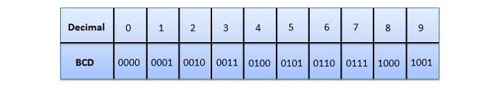
Advantages of BCD Codes
- BCD codes are very similar to the decimal system.
- We need to remember the binary equivalent of the decimal numbers 0 to 9 only.
Disadvantages of BCD Codes
- The addition and subtraction of BCD codes follow different rules.
- BCD arithmetic is a little more complicated.
- BCD needs more number of bits than binary to represent the decimal number. So, BCD is less efficient than binary.
Error Detecting Codes
Error detecting codes are special types of binary codes used to identify errors in digital communication and data storage. Error detecting codes add redundancy to the data that allows receiver to identify if there is any error occurred. Common examples of error detecting codes include parity bit, checksum, hamming code, etc.
Error detecting codes are important to ensure integrity in data transmission and storage. They help in improving the reliability of the system.
What are Errors?
An error is a condition when the output information does not match with the input information. During transmission, digital signals suffer from noise that can introduce errors in the binary bits travelling from one system to other. That means a 0 bit may change to 1 or a 1 bit may change to 0.

Whenever a message is transmitted, it may get scrambled by noise or data may get corrupted. To avoid this, we use error-detecting codes which are additional data added to a given digital message to help us detect if an error occurred during transmission of the message. A simple example of error-detecting code is parity check.
Error Correcting Codes
Error correcting codes are binary codes designed to correct the errors occurred in a digital system during data transmission or storage. Error correcting codes add some additional information to the data to be transmitted or stored.
Error-correcting codes deploy the same strategy as error-detecting codes but additionally, such codes also detect the exact location of the corrupt bit. This allows the receiver to re-obtain the original data even if some of the bits are corrupted.
In error-correcting codes, parity check has a simple way to detect errors along with a sophisticated mechanism to determine the corrupt bit location. Once the corrupt bit is located, its value is reverted (from 0 to 1 or 1 to 0) to get the original message.
Just like error detecting codes, error correcting codes are important to maintain data integrity in digital communication and data storage applications.
Different types of error correcting codes are used in different digital systems depending on the type of communication channel, error pattern, degree of error correction, etc. Some common examples of error correcting codes are Hamming code, Reed-Solomon code, Low-Density-Parity-Check code, BCH code, etc.
How to Detect and Correct Errors?
To detect and correct the errors, additional bits are added to the data bits at the time of transmission.
- The additional bits are called parity bits. They allow detection or correction of the errors.
- The data bits along with the parity bits form a code word.
Parity Checking of Error Detection
It is the simplest technique for detecting and correcting errors. The MSB of an 8-bits word is used as the parity bit and the remaining 7 bits are used as data or message bits. The parity of 8-bits transmitted word can be either even parity or odd parity.

Even Parity − Even parity means the number of 1's in the given word including the parity bit should be even (2,4,6,....).
Odd Parity − Odd parity means the number of 1's in the given word including the parity bit should be odd (1,3,5,....).
Use of Parity Bit
The parity bit can be set to "0" or "1" depending on the type of the parity required.
For even parity, this bit is set to 1 or 0 such that the number of "1 bits" in the entire word is even. See Fig. (a).
For odd parity, this bit is set to 1 or 0 such that the number of "1 bits" in the entire word is odd. See Fig. (b).

How Does Error Detection Take Place?
Parity checking at the receiver can detect the presence of an error if the parity of the receiver signal is different from the expected parity. That means, if it is known that the parity of the transmitted signal is always going to be "even" and if the received signal has an odd parity, then the receiver can conclude that the received signal is not correct.
If an error is detected, then the receiver will ignore the received byte and request for retransmission of the same byte to the transmitter.

Advantages of Binary Codes
Binary codes have several advantages in the field of digital electronics. Here are the key benefits of using binary codes −
- Simplicity − Binary codes use only two digits, i.e., 0 and 1 to represent information. It simplifies the electronic circuit design and implementation.
- Ease in Implementation − Binary codes use only two states namely, on and off. So, their implementation is straightforward.
- Ease of Storage − Binary codes are easy to store in digital memory devices like hard disk, CD, DVD, pen drive, etc. They require compact storage at higher efficiency.
- Easy and Fast Processing − Binary codes can be efficiently processed using digital systems having an arithmetic and logic unit. They allow fast and error-free computing.
- Easy Communication − Binary codes provide an efficient method of information transmission at a very high speed. Various error detecting and correcting techniques can be applied to binary codes that make the digital communication more efficient.
- Easy Scalability − Binary codes provide easy scalability of a digital system. We can increase the range of a digital system just by adding more bits in the code.
- Compatibility − Binary codes are compatible with a wide range of digital devices and systems.
- Reliability − Binary codes are highly immune to noise and interference that provide improved reliability in the digital system.
Disadvantages of Binary Codes
Binary codes have several advantages as given above. However, they also have some disadvantages and limitations.
Some key disadvantages of binary codes are listed below −
- Binary codes are not human friendly. For human beings, reading and interpreting binary codes can be a complex task.
- In some situations, binary codes have to be converted into other number systems that adds extra computational overhead to the system.
- Binary codes require higher transmission bandwidth in communication channel.
- In binary codes, it is quite difficult to identify the errors. It becomes more challenging in case of long binary sequences.
Applications of Binary Codes
Binary codes are widely used in various fields of digital electronics due to their high efficiency in information representation.
Listed below are some of the key applications of binary codes −
- Digital Computers − Binary codes are primarily used in digital computer to represent information and instructions.
- Digital Communication − Binary codes are also used for transmission of data and information using digital channels.
- Digital Displays − Binary codes are also used to display numbers and alphabets in digital systems.
- Barcode Systems − Binary codes are also used in barcode systems for product identification and inventory management. In this system, bars of different width and spaces between them represent binary digits that can be interpreted by a scanner.
- Data Storage − Binary codes are used to store information in digital devices like computer memory.
- Digital Control Systems − Binary codes are used to program a digital control system. In a digital control system, binary codes are used to represent different types of control signals and instructions used for automation.
- Computer Graphics − Binary codes are also used in computer graphics to represent colors, shapes, pixel values, and other information.
Conclusion
In conclusion, binary codes are one of the crucial components of a digital system. They are used to represent information and instructions in digital format. There are several different types of binary codes used in digital electronics.
Different binary codes are used for different purposes depending on the nature of application. For example, ASCII code is used for alphanumeric data representation. In this chapter, we explained the basic concepts of binary codes. In the upcoming chapters, we will explore the different types of binary codes and their applications in digital electronics.
What is 8421 BCD Code?
The 8421 BCD code is one of the most commonly used binary codes in the field of digital electronics. This binary code is used to encode decimal digits from 0 to 9 in their equivalent binary format.
Read this chapter to learn all about 8421 BCD codes including its advantages, limitations, and applications.
What is 8421 BCD Code?
In digital electronics, the 8421 BCD code is a type of binary code. BCD stands for Binary Coded Decimal. The 8421 BCD code is the most widely used binary code for expressing decimal numbers in their equivalent binary format.
The 8421 BCD code is also known as the natural BCD code. It is a binary code used to represent each decimal digit by using a unique combination of 4-bits. It is a weighted binary code and is also a sequential binary code.
The digits 8421 represents the weights assigned to each of the four bits, where the most significant bit has a weight of 8 and the least significant bit has a weight of 1.
In the 8421 BCD code, each decimal digit can be represented by a unique 4-bit binary code. The following table highlights the 8421 BCD code for each decimal digit.
| Decimal Digit | 8421 BCD Code |
|---|---|
| 0 | 0000 |
| 1 | 0001 |
| 2 | 0010 |
| 3 | 0011 |
| 4 | 0100 |
| 5 | 0101 |
| 6 | 0110 |
| 7 | 0111 |
| 8 | 1000 |
| 9 | 1001 |
The 8421 BCD code is the most commonly used code in digital electronics to represent decimal numbers in binary form. It is mainly used in digital devices where human machine interface is required.
Advantages of 8421 BCD Code
In digital electronics, the 8421 BCD code has several advantages, mainly in applications where decimal numbers are used in a digital system. Some of the key benefits of the 8421 BCD code are given below −
- The 8421 BCD code provides a natural way of representing decimal numbers. This is because, we can directly encode each decimal digit into its equivalent 4-bit binary number.
- The 8421 BCD code allows for simple conversion between decimal and binary number systems. Hence, it is quite useful in digital devices where human input is required.
- The 8421 BCD code simplifies the arithmetic operations such as addition, subtraction, multiplication, and division of decimal numbers using a digital system like a calculator.
- The 8421 BCD code is compatible with decimal displays. Hence, it is commonly used in digital devices where the output has to be displayed on a decimal-based display like 7-segment display.
All these are the main advantages of 8421 BCD code. However, there are also some disadvantages of 8421 BCD code, lets discuss them.
Disadvantages of 8421 BCD Code
Listed below are some of the major disadvantages of using the 8421 BCD code −
- The 8421 BCD code is relatively less efficient than the pure binary code, as it requires a greater number of bits to represent a decimal number. For example, the decimal number 15 can be represented as 1111 in pure binary, whereas 0001 0101 in 8421 BCD.
- The arithmetic operations such as addition, subtraction, multiplication, and division performed in 8421 BCD code are relative more complex than they are in pure binary.
- The 8421 BCD code consumes more storage space as it uses 4 bits to represent each decimal digit.
- In the case of 8421 BCD code arithmetic, the rules of binary arithmetic cannot be applied to the entire 8421 BCD number, but only to the individual groups of 4-bits.
- The 8421 BCD codes are not suitable in applications where speed and efficiency are critical.
- In 8421 BCD code, there are six illegal code combinations. They are 1010, 1011, 1100, 1101, 1110, and 1111.
Thus, all these are the main disadvantages of the 8421 BCD code.
Applications of 8421 BCD Code
The 8421 BCD code is widely used in various applications in digital electronics. Given below are some of the key applications of the 8421 BCD code −
The 8421 BCD code is mainly used in digital displays used in calculators, digital clocks and watches, etc. where decimal digits are to be displayed.
- The 8421 BCD code is also used in device that accept numeric inputs like calculators.
- In process control systems, the 8421 BCD code is used to represent and manipulate the decimal values.
- The 8421 BCD codes are also used in embedded systems where human machine interaction is critical.
- The 8421 BCD code is widely used in control panels of various electronic devices to display numerical values.
This is all about the basics of the 8421 BCD code. In the next section, we will explain how you can perform addition and subtraction of 8421 BCD codes.
Addition in 8421 BCD Code
The addition operations in 8421 BCD code are performed by individually adding the corresponding digits of the given decimal numbers expressed in 4-bit binary form.
In BCD addition, if there is no end-around carry, the sum is not an illegal BCD code. Thus, it does not require any correction.
If there is an end-around carry from one group to the next group, of if the sum is an illegal code, then it is corrected by adding 0110 to the sum term and the resulting carry is added to the next group.
Let us understand the BCD addition with the help of an example.
Example
Add 251 and 353 in the 8421 BCD code.
Solution
Converting the given decimal numbers into BCD code,
251 = 0010 0101 0001
353 = 0011 0101 0011
Adding the BCD codes,

Hence, the sum of 251 and 353 is 604.
Subtraction in 8421 BCD Code
To perform subtraction of decimal numbers using 8421 BCD code, we first convert the given decimal numbers into their 8421 BCD codes. Then, we subtract the BCD subtrahend from the BCD minuend starting from the LSD.
If there is no borrow from the next higher group, then no correction is needed. If there is a borrow from the next higher group, then the result has to be obtained by subtracting 0110 from the intermediate difference term.
Let us take an example to understand the BCD subtraction.
Example
Subtract 15 from 25 in 8421 BCD code.
Solution
Converting the given decimal number into BCD code,
25 = 0010 0101
15 = 0001 0101
Subtracting the BCD code,

Hence, the difference of 25 and 15 is 10.
Conclusion
In conclusion, the 8421 BCD code is a natural binary coded decimal code widely used in digital electronics. It is primarily used in applications where decimal digits and human interaction are critical.
The most significant advantage of the 8421 BCD code is that it provides an easy conversion to and from decimal numbers. But it is less space efficient code because it requires more bits to represent a decimal digit.
What is Excess-3 Code?
Excess-3 code is a non-weighted BCD (Binary Coded Decimal) code. It is called excess-3 code because it is obtained by adding 0011 (3) to the 8421 BCD code. Also called XS-3, the excess 3 code is a BCD code that represents each decimal digit as a 4-bit binary code.
The excess-3 binary code is a sequential code, so we can use it to perform arithmetic operations. Also, it is a self-complementing code, therefore the subtraction operation by the complement method is simpler than that in the 8421 BCD code.
However, in the excess-3 code, there are six invalid codes, they are 0000, 0001, 0010, 1110, and 1111.
How to Obtain Excess-3 Code?
We can obtain the excess-3 code by adding 0011 (3) to the natural 8421 BCD code. It is explained here −
Decimal digit = 0
8421 BCD code = 0000
Excess-3 code = 0000 + 0011 = 0011

Decimal digit = 1
8421 BCD code = 0001
Excess-3 code = 0001 + 0011 = 0100
Similarly, we can obtain the excess-3 code for all the decimal digits.
The following table shows the excess-3 code for each decimal digit −
| Decimal Digit | Excess-3 Code |
|---|---|
| 0 | 0011 |
| 1 | 0100 |
| 2 | 0101 |
| 3 | 0110 |
| 4 | 0111 |
| 5 | 1000 |
| 6 | 1001 |
| 7 | 1010 |
| 8 | 1011 |
| 9 | 1100 |
Note − The Excess-3 code is not so widely used today. It was mainly used in early digital systems. Nowadays, many other advanced and efficient binary codes are being used in place of the excess-3 code.
Importance of Excess-3 Code in Digital Electronics
Excess-3 code is one of the widely used binary codes in early digital systems. Here are some of the key reasons why excess-3 code was used in the field of digital electronics −
- It provides a simplified way of converting a decimal number into binary code.
- It has self-complementing property that makes it suitable for error detection and correction applications.
- It is sequential code, hence it can be used to perform arithmetic operations in digital systems.
- Excess-3 code is highly compatible with decimal IO devices. Thus, it provides a convenient interface between digital systems and other devices.
Advantages of Excess-3 Code
Although, the excess-3 code is less common in modern digital systems. But it has the following key benefits over other binary coding schemes −
- Excess-3 code provides an easy method of representing decimal numbers in binary form.
- Excess-3 code provides an easier way of performing addition and subtraction operations without using any complex conversion methods.
- Excess-3 code is quite easy to convert to and from decimal numbers.
- Excess-3 code being a binary-coded decimal is highly compatible with a wide range of decimal devices.
Disadvantages of Excess-3 Code
Excess-3 code has several advantages, but it also has certain disadvantages as well thats why it is less commonly used in modern digital systems. The following are some key disadvantages of excess-3 code −
- Excess-3 code is an inefficient binary representation of decimal numbers as compared to pure binary. This is because it requires more bits to represent a decimal digit.
- Excess-3 code requires additional arithmetic circuit to add 3 to the standard binary code.
- Excess-3 code has limited compatibility with pure binary systems.
Applications of Excess-3 Code
Excess-3 code was widely used in early digital systems and digital computers. The key areas of excess-3 code applications are listed below −
- Excess-3 code was used in early digital computers.
- Excess-3 code is also used in decimal data processing through digital systems.
- Excess-3 code is also used in digital devices likes printers, card readers, etc. where decimal data is employed.
- The self-complementing property of excess-3 code makes it suitable to use in error detection and correction applications.
- Excess-3 code is also communication and data transmission applications.
Excess-3 Addition
In excess-3 addition, starting from LSD (least significant digit), we add the 4-bit group in each column.
If no end-around carry is generated from the addition of 4-bit group, we have to subtract 0011 from the sum term to obtain the result. This is because, no carry means the result is in XS-6 format. Thus, we obtain the correct sum by adding 0011 to the sum term.
If an end-around carry is produced from the addition, we have to add 0011 to the sum term to obtain the corrected result. This is because the carry out represents that the sum term is an invalid excess-3 code, which is corrected by adding 0011 to the sum term.
Let us understand the XS-3 addition with the help of examples.
Example
Add 35 and 28 in XS-3 code.
Solution
The given decimal numbers and their XS-3 code are
35 = 0110 1000
28 = 0101 1011
Adding the XS-3 codes,

Hence, the correct sum of 35 and 28 is 1001 0110 in XS-3 and 63 in decimal.
Excess-3 Subtraction
In the XS-3 subtraction, starting from the least significant digit, we find the difference of two numbers by subtracting each group of 4-bits of subtrahend from he corresponding 4-bit group of the minuend.
In the XS-3 subtraction, if there is no borrow from the higher 4-bit group, then we add 0011 to the difference term to obtain the corrected result. This is because if there is no borrow, then the result is in the normal binary that has to be converted into XS-3 by adding 0011 to it.
If a borrow is taken from the next 4-bit group, then the difference term will be an invalid XS-3 code which is corrected by subtracting 0011 from it.
Let us understand the XS-3 subtraction through a solved example.
Example
Subtract 28 from 56 in XS-3 code.
Solution
Given,
Minuend = (56)10 = (1000 1001)XS-3
Subtrahend = (28)10 = (0101 1011)XS-3
Subtracting in the XS-3 code, we get,

Hence, the corrected difference of the numbers 56 and 28 is 0101 1011 in XS-3 code and 28 in decimal.
Conclusion
In conclusion, the Excess-3 (XS-3) code is a binary coding scheme widely used in old digital systems. It is basically a BCD scheme used to represent decimal digits in binary format.
In modern digital systems, the excess-3 code is replaced by more efficient binary codes like 8421 BCD code, ASCII code, etc.
What is Gray Code?
The gray code is a type of reflective and unit distance binary code widely used in the field of digital electronics.
It is important to note that the gray code is not a binary coded decimal (BCD) code. Thus, it cannot be used to directly represent a decimal number. It is also not a weighted code, therefore, we cannot use it to perform arithmetic operations.
In gray codes, the successive code words differ in one bit position only, hence it is a cyclic code or a unit distance code. The cyclic or reflective property of gray codes make it suitable to use in applications like error minimization in rotary encoders, communication systems, analog to digital converters, etc.
Gray Codes Table
The following table shows 1-bit, 2-bit, 3-bit, and 4-bit gray codes and their reflective nature −
| Gray Codes | |||
|---|---|---|---|
| 1-Bit | 2-Bit | 3-Bit | 4-Bit |
| 0 | 00 | 000 | 0000 |
| 1 | 01 | 001 | 0001 |
| 11 | 011 | 0011 | |
| 10 | 010 | 0010 | |
| 110 | 0110 | ||
| 111 | 0111 | ||
| 101 | 0101 | ||
| 100 | 0100 | ||
| 1100 | |||
| 1101 | |||
| 1111 | |||
| 1110 | |||
| 1010 | |||
| 1011 | |||
| 1001 | |||
| 1000 | |||
Importance of Gray Code
The gray code is one of the most popular reflective codes or unit distance codes. In digital electronics, it is important due to the following main reasons −
- In gray code, only one-bit changes when moving from one word to the next i.e., two consecutive numbers differ in one bit only. This characteristic of the gray code minimizes the errors during transition.
- The unit distance property of gray code allows it to use in rotary encoder for accurate position detection.
- Gray code reduces the errors significantly in analog to digital signal conversion.
- Gray code also helps to reduce the impact of signal noise in communication systems.
- In data storage and transmission, gray code plays an important role in detecting and correcting errors.
- In gray code, only bit changes at each transition. It is used to implement digital systems that consume less power.
Overall, the gray code is an important type of reflective code in digital electronics and it is widely used in various digital electronic devices and systems.
Advantages of Gray Code
In digital electronics, the gray code has several advantages over other types of binary codes. The following are some major benefits of gray code −
- Gray code minimizes the error during transition. This is because, it has two consecutive codes differ in one bit only.
- Gray code reduces the chances of errors in readings during position detection in rotary encoders.
- In gray code, only one-bit changes at a time, this property eliminates the problem of technical glitch and electromagnetic interference.
- In digital communication, the gray code can detect and correct errors, and hence improves the signal integrity.
- Being a unit distance code, the gray code provides a smooth transition from one state to the next.
- In analog to digital conversion, gray code helps minimize the errors in sampling of analog signals.
- Gray code based digital systems consume less power than a system in which multiple bit changes simultaneously.
Disadvantages of Gray Code
Apart from advantages, gray code also has several disadvantages. Some key disadvantages of gray codes are described below −
- Gray code involves more complex conversion process between binary and gray codes.
- Digital circuits that work with gray code are relatively more complex and expensive to design and implement.
- Gray code has limited natural ordering making it difficult to interpret by humans.
- Gray code is a non-weighted code. Hence, it is not suitable to perform arithmetic operations.
- Gray code arithmetic is relatively more complex than other binary codes.
- Gray code is not suitable to use in general purpose digital computing systems.
- Gray code is not a universally adopted binary coding scheme due to some specific requirements of the applications.
Applications of Gray Code
In digital electronics, gray code is used in several applications where reflective and unit distance properties are critical. The following are some main applications of gray code −
- Gray code is used in rotary encoders for accurate position detection.
- Gray code is also used in analog to digital converters for error-free sampling of analog signals.
- Gray codes are used in error detection and correction algorithms utilized in data storage and transmission systems.
- Gray code is used in digital circuits where smooth and sequential switching is desired.
- Gray code is used in digital devices like bar code scanners to encode information.
- In the field robotics and automation, gray code is used to determine the position of robotic joints.
- In electronic devices and systems, gray codes are used for sequential switching.
Conclusion
In conclusion, gray code, also known as reflective code or unit distance code, is a non-weighted binary code used in different areas of digital electronics. Gray code is not a universally adopted binary code, but it is mainly used in applications where the unit distance property is desired.
Digital Electronics - ASCII Codes
ASCII stands for American Standard Code for Information Interchange. The ASCII code is a popular coding scheme used in digital computing systems to encode characters.
In the ASCII code, a unique integer value is assigned to each character like number, letter, symbol, etc. The standard ASCII code defines a set of 128 characters, where each character can be represented by a unique 7-bit binary code. Therefore, ASCII code can represent total 27 = 128 possible characters.
In digital electronics, the characters in ASCII code are generally represented in decimal or hexadecimal notation. Overall, the ASCII code is a standard encoding scheme for representing characters in digital computers and communication systems.
Properties of ASCII Code
The following are some key characteristics of ASCII code −
- ASCII code assigns a unique numeric value to each character.
- ASCII code provides a way of representing letters, numbers, symbols, and control characters.
- ASCII code is compatible with a wide range of programming languages and digital devices.
- ASCII code supports various control characters for basic text formatting and device control.
- ASCII code has decimal and hexadecimal representation. Hence, it is human-readable.
- ASCII code assigns numeric values to characters in a sequential order, making it an efficient encoding standard in terms of sorting and searching.
- ASCII code is highly space efficient and simple.
Types of ASCII Code
ASCII (American Standard Code for Information Interchange) code is basically a 7-bit character encoding standard used in digital electronics. But it is evolved with the advancement in computing technologies.
The following are two main types of ASCII codes −
- Standard ASCII Code
- Extended ASCII Code
Let's discuss the Standard ASCII Codes first.
Standard ASCII Code
It is a 7-bit character encoding standard having a range from 0 to 127 i.e., total 128 possible characters. It assigns a 7-bit unique binary code to each character including numbers, letters, symbols, and control characters.
The following table highlights the name, symbol and ASCII code in decimal and binary form for the range from 0 to 127.
| Name | Symbol | Decimal | 7-Bit Binary |
|---|---|---|---|
| Null char | NUL | 0 | 00000000 |
| Start of Heading | SOH | 1 | 00000001 |
| Start of Text | STX | 2 | 00000010 |
| End of Text | ETX | 3 | 00000011 |
| End of Transmission | EOT | 4 | 00000100 |
| Enquiry | ENQ | 5 | 00000101 |
| Acknowledgment | ACK | 6 | 00000110 |
| Bell | BEL | 7 | 00000111 |
| Back Space | BS | 8 | 00001000 |
| Horizontal Tab | HT | 9 | 00001001 |
| Line Feed | LF | 10 | 00001010 |
| Vertical Tab | VT | 11 | 00001011 |
| Form Feed | FF | 12 | 00001100 |
| Carriage Return | CR | 13 | 00001101 |
| Shift Out / X-On | SO | 14 | 00001110 |
| Shift In / X-Off | SI | 15 | 00001111 |
| Data Line Escape | DLE | 16 | 00010000 |
| Device Control 1 (oft. XON) | DC1 | 17 | 00010001 |
| Device Control 2 | DC2 | 18 | 00010010 |
| Device Control 3 (oft. XOFF) | DC3 | 19 | 00010011 |
| Device Control 4 | DC4 | 20 | 00010100 |
| Negative Acknowledgement | NAK | 21 | 00010101 |
| Synchronous Idle | SYN | 22 | 00010110 |
| End of Transmit Block | ETB | 23 | 00010111 |
| Cancel | CAN | 24 | 00011000 |
| End of Medium | EM | 25 | 00011001 |
| Substitute | SUB | 26 | 00011010 |
| Escape | ESC | 27 | 00011011 |
| File Separator | FS | 28 | 00011100 |
| Group Separator | GS | 29 | 00011101 |
| Record Separator | RS | 30 | 00011110 |
| Unit Separator | US | 31 | 00011111 |
| Space | 32 | 00100000 | |
| Exclamation mark | ! | 33 | 00100001 |
| Double quotes | " | 34 | 00100010 |
| Hash | # | 35 | 00100011 |
| Dollar | $ | 36 | 00100100 |
| Percentage | % | 37 | 00100101 |
| Ampersand | & | 38 | 00100110 |
| Single quote | ' | 39 | 00100111 |
| Open parenthesis | ( | 40 | 00101000 |
| Close parenthesis | ) | 41 | 00101001 |
| Asterisk | * | 42 | 00101010 |
| Plus | + | 43 | 00101011 |
| Comma | , | 44 | 00101100 |
| Hyphen | - | 45 | 00101101 |
| Period, dot or full stop | . | 46 | 00101110 |
| Slash or divide | / | 47 | 00101111 |
| Zero | 0 | 48 | 00110000 |
| One | 1 | 49 | 00110001 |
| Two | 2 | 50 | 00110010 |
| Three | 3 | 51 | 00110011 |
| Four | 4 | 52 | 00110100 |
| Five | 5 | 53 | 00110101 |
| Six | 6 | 54 | 00110110 |
| Seven | 7 | 55 | 00110111 |
| Eight | 8 | 56 | 00111000 |
| Nine | 9 | 57 | 00111001 |
| Colon | : | 58 | 00111010 |
| Semicolon | ; | 59 | 00111011 |
| Less than | < | 60 | 00111100 |
| Equals | = | 61 | 00111101 |
| Greater than | > | 62 | 00111110 |
| Question mark | ? | 63 | 00111111 |
| At symbol | @ | 64 | 01000000 |
| Uppercase A | A | 65 | 01000001 |
| Uppercase B | B | 66 | 01000010 |
| Uppercase C | C | 67 | 01000011 |
| Uppercase D | D | 68 | 01000100 |
| Uppercase E | E | 69 | 01000101 |
| Uppercase F | F | 70 | 01000110 |
| Uppercase G | G | 71 | 01000111 |
| Uppercase H | H | 72 | 01001000 |
| Uppercase I | I | 73 | 01001001 |
| Uppercase J | J | 74 | 01001010 |
| Uppercase K | K | 75 | 01001011 |
| Uppercase L | L | 76 | 01001100 |
| Uppercase M | M | 77 | 01001101 |
| Uppercase N | N | 78 | 01001110 |
| Uppercase O | O | 79 | 01001111 |
| Uppercase P | P | 80 | 01010000 |
| Uppercase Q | Q | 81 | 01010001 |
| Uppercase R | R | 82 | 01010010 |
| Uppercase S | S | 83 | 01010011 |
| Uppercase T | T | 84 | 01010100 |
| Uppercase U | U | 85 | 01010101 |
| Uppercase V | V | 86 | 01010110 |
| Uppercase W | W | 87 | 01010111 |
| Uppercase X | X | 88 | 01011000 |
| Uppercase Y | Y | 89 | 01011001 |
| Uppercase Z | Z | 90 | 01011010 |
| Opening bracket | [ | 91 | 01011011 |
| Backslash | \ | 92 | 01011100 |
| Closing bracket | ] | 93 | 01011101 |
| Caret - circumflex | ^ | 94 | 01011110 |
| Underscore | _ | 95 | 01011111 |
| Grave accent | ` | 96 | 01100000 |
| Lowercase a | a | 97 | 01100001 |
| Lowercase b | b | 98 | 01100010 |
| Lowercase c | c | 99 | 01100011 |
| Lowercase d | d | 100 | 01100100 |
| Lowercase e | e | 101 | 01100101 |
| Lowercase f | f | 102 | 01100110 |
| Lowercase g | g | 103 | 01100111 |
| Lowercase h | h | 104 | 01101000 |
| Lowercase i | i | 105 | 01101001 |
| Lowercase j | j | 106 | 01101010 |
| Lowercase k | k | 107 | 01101011 |
| Lowercase l | l | 108 | 01101100 |
| Lowercase m | m | 109 | 01101101 |
| Lowercase n | n | 110 | 01101110 |
| Lowercase o | o | 111 | 01101111 |
| Lowercase p | p | 112 | 01110000 |
| Lowercase q | q | 113 | 01110001 |
| Lowercase r | r | 114 | 01110010 |
| Lowercase s | s | 115 | 01110011 |
| Lowercase t | t | 116 | 01110100 |
| Lowercase u | u | 117 | 01110101 |
| Lowercase v | v | 118 | 01110110 |
| Lowercase w | w | 119 | 01110111 |
| Lowercase x | x | 120 | 01111000 |
| Lowercase y | y | 121 | 01111001 |
| Lowercase z | z | 122 | 01111010 |
| Opening brace | { | 123 | 01111011 |
| Vertical bar | | | 124 | 01111100 |
| Closing brace | } | 125 | 01111101 |
| Equivalency sign (tilde) | ~ | 126 | 01111110 |
| Delete | 127 | 01111111 |
Extended ASCII Code
It is an 8-bit character encoding standard having a range from 0 to 255 i.e., total 256 possible characters. The extended ASCII code adds extra 128 characters to the standard ASCII code.
The following table shows the name, symbol and ASCII code in decimal and binary form for the range from 128 to 255.
| Name | Symbol | DEC | BIN |
|---|---|---|---|
| Euro sign | 128 | 10000000 | |
| 129 | 10000001 | ||
| Single low-9 quotation mark | 130 | 10000010 | |
| Latin small letter f with hook | 131 | 10000011 | |
| Double low-9 quotation mark | 132 | 10000100 | |
| Horizontal ellipsis | 133 | 10000101 | |
| Dagger | 134 | 10000110 | |
| Double dagger | 135 | 10000111 | |
| Modifier letter circumflex accent | 136 | 10001000 | |
| Per mille sign | 137 | 10001001 | |
| Latin capital letter S with caron | 138 | 10001010 | |
| Single left-pointing angle quotation | 139 | 10001011 | |
| Latin capital ligature OE | 140 | 10001100 | |
| 141 | 10001101 | ||
| Latin capital letter Z with caron | 142 | 10001110 | |
| 143 | 10001111 | ||
| 144 | 10010000 | ||
| Left single quotation mark | 145 | 10010001 | |
| Right single quotation mark | 146 | 10010010 | |
| Left double quotation mark | 147 | 10010011 | |
| Right double quotation mark | 148 | 10010100 | |
| Bullet | 149 | 10010101 | |
| En dash | 150 | 10010110 | |
| Em dash | 151 | 10010111 | |
| Small tilde | 152 | 10011000 | |
| Trade mark sign | 153 | 10011001 | |
| Latin small letter S with caron | 154 | 10011010 | |
| Single right-pointing angle quotation mark | 155 | 10011011 | |
| Latin small ligature oe | 156 | 10011100 | |
| 157 | 10011101 | ||
| Latin small letter z with caron | 158 | 10011110 | |
| Latin capital letter Y with diaeresis | 159 | 10011111 | |
| Non-breaking space | 160 | 10100000 | |
| Inverted exclamation mark | 161 | 10100001 | |
| Cent sign | 162 | 10100010 | |
| Pound sign | 163 | 10100011 | |
| Currency sign | 164 | 10100100 | |
| Yen sign | 165 | 10100101 | |
| Pipe, Broken vertical bar | 166 | 10100110 | |
| Section sign | 167 | 10100111 | |
| Spacing diaeresis - umlaut | 168 | 10101000 | |
| Copyright sign | 169 | 10101001 | |
| Feminine ordinal indicator | 170 | 10101010 | |
| Left double angle quotes | 171 | 10101011 | |
| Not sign | 172 | 10101100 | |
| Soft hyphen | 173 | 10101101 | |
| Registered trade mark sign | 174 | 10101110 | |
| Spacing macron - overline | 175 | 10101111 | |
| Degree sign | 176 | 10110000 | |
| Plus-or-minus sign | 177 | 10110001 | |
| Superscript two - squared | 178 | 10110010 | |
| Superscript three - cubed | 179 | 10110011 | |
| Acute accent - spacing acute | 180 | 10110100 | |
| Micro sign | 181 | 10110101 | |
| Pilcrow sign - paragraph sign | 182 | 10110110 | |
| Middle dot - Georgian comma | 183 | 10110111 | |
| Spacing cedilla | 184 | 10111000 | |
| Superscript one | 185 | 10111001 | |
| Masculine ordinal indicator | 186 | 10111010 | |
| Right double angle quotes | 187 | 10111011 | |
| Fraction one quarter | 188 | 10111100 | |
| Fraction one half | 189 | 10111101 | |
| Fraction three quarters | 190 | 10111110 | |
| Inverted question mark | 191 | 10111111 | |
| Latin capital letter A with grave | 192 | 11000000 | |
| Latin capital letter A with acute | 193 | 11000001 | |
| Latin capital letter A with circumflex | 194 | 11000010 | |
| Latin capital letter A with tilde | 195 | 11000011 | |
| Latin capital letter A with diaeresis | 196 | 11000100 | |
| Latin capital letter A with ring above | 197 | 11000101 | |
| Latin capital letter AE | 198 | 11000110 | |
| Latin capital letter C with cedilla | 199 | 11000111 | |
| Latin capital letter E with grave | 200 | 11001000 | |
| Latin capital letter E with acute | 201 | 11001001 | |
| Latin capital letter E with circumflex | 202 | 11001010 | |
| Latin capital letter E with diaeresis | 203 | 11001011 | |
| Latin capital letter I with grave | 204 | 11001100 | |
| Latin capital letter I with acute | 205 | 11001101 | |
| Latin capital letter I with circumflex | 206 | 11001110 | |
| Latin capital letter I with diaeresis | 207 | 11001111 | |
| Latin capital letter ETH | 208 | 11010000 | |
| Latin capital letter N with tilde | 209 | 11010001 | |
| Latin capital letter O with grave | 210 | 11010010 | |
| Latin capital letter O with acute | 211 | 11010011 | |
| Latin capital letter O with circumflex | 212 | 11010100 | |
| Latin capital letter O with tilde | 213 | 11010101 | |
| Latin capital letter O with diaeresis | 214 | 11010110 | |
| Multiplication sign | 215 | 11010111 | |
| Latin capital letter O with slash | 216 | 11011000 | |
| Latin capital letter U with grave | 217 | 11011001 | |
| Latin capital letter U with acute | 218 | 11011010 | |
| Latin capital letter U with circumflex | 219 | 11011011 | |
| Latin capital letter U with diaeresis | 220 | 11011100 | |
| Latin capital letter Y with acute | 221 | 11011101 | |
| Latin capital letter THORN | 222 | 11011110 | |
| Latin small letter sharp s - ess-zed | 223 | 11011111 | |
| Latin small letter a with grave | 224 | 11100000 | |
| Latin small letter a with acute | 225 | 11100001 | |
| Latin small letter a with circumflex | 226 | 11100010 | |
| Latin small letter a with tilde | 227 | 11100011 | |
| Latin small letter a with diaeresis | 228 | 11100100 | |
| Latin small letter a with ring above | 229 | 11100101 | |
| Latin small letter ae | 230 | 11100110 | |
| Latin small letter c with cedilla | 231 | 11100111 | |
| Latin small letter e with grave | 232 | 11101000 | |
| Latin small letter e with acute | 233 | 11101001 | |
| Latin small letter e with circumflex | 234 | 11101010 | |
| Latin small letter e with diaeresis | 235 | 11101011 | |
| Latin small letter i with grave | 236 | 11101100 | |
| Latin small letter i with acute | 237 | 11101101 | |
| Latin small letter i with circumflex | 238 | 11101110 | |
| Latin small letter i with diaeresis | 239 | 11101111 | |
| Latin small letter eth | 240 | 11110000 | |
| Latin small letter n with tilde | 241 | 11110001 | |
| Latin small letter o with grave | 242 | 11110010 | |
| Latin small letter o with acute | 243 | 11110011 | |
| Latin small letter o with circumflex | 244 | 11110100 | |
| Latin small letter o with tilde | 245 | 11110101 | |
| Latin small letter o with diaeresis | 246 | 11110110 | |
| Division sign | 247 | 11110111 | |
| Latin small letter o with slash | 248 | 11111000 | |
| Latin small letter u with grave | 249 | 11111001 | |
| Latin small letter u with acute | 250 | 11111010 | |
| Latin small letter u with circumflex | 251 | 11111011 | |
| Latin small letter u with diaeresis | 252 | 11111100 | |
| Latin small letter y with acute | 253 | 11111101 | |
| Latin small letter thorn | 254 | 11111110 | |
| Latin small letter y with diaeresis | 255 | 11111111 |
Advantages of ASCII Code
The following are the key benefits of the ASCII (American Standard Code for Information Interchange) code −
- The ASCII code provides a simple and straightforward encoding scheme to represent letters, numbers, and symbols.
- ASCII code is compatible with a wide range of programming languages and computing devices.
- ASCII code provides a compact character representation, where each character can be represented using 7-bits or 8-bits. Hence, it is a space efficient encoding standard.
- ASCII code is a universally adopted encoding standard in the field of digital electronics.
- ASCII code has easy and simple implementation in hardware and software.
Limitations of ASCII Code
ASCII code has several advantages as described above, but it also has some limitations which are given below −
- The standard ASCII code has a limited set of 128 characters. This makes it unsuitable for representing characters of languages other than English.
- The ASCII code can be extended to 8-bits but it is not standardized beyond 7-bits.
- ASCII code is not suitable to use in systems that require a broad range of characters.
Applications of ASCII Code
ASCII code is a standard character encoding scheme used in wide range of applications in the field of digital electronics.
Some major applications of ASCII code are listed below −
- ASCII code is used in digital systems for textual communication.
- ASCII code is used in computer programming to represent alphanumeric data like letters, numbers, symbols, etc.
- ASCII code is also used in various communication protocols utilized for data transmission among devices.
- In the field web technology, ASCII code is used to represent different characters and symbols in a webpage.
- ASCII code is also used in database systems to represent text data.
Conclusion
In conclusion, ASCII (American Standard Code for Information Interchange) is a character encoding scheme widely used in digital systems. It is a 7-bit standard code used to represent a total of 128 characters including numbers, letters, symbols, and control characters.
What is EBCDIC Code?
The EBCDIC (Extended Binary Coded Decimal Interchange Code) is an alphanumeric code used in digital systems to represent alphanumeric characters, such as letters, numbers, symbols, etc.
EBCDIC is pronounced as "eb-si-dik". It is an 8-bit binary coded used for representing alphanumeric data in digital systems.
Here, we will explain the EBCDIC code in detail along with its advantages and applications.
What is EBCDIC Code?
EBCDIC stands for Extended Binary Coded Decimal Interchange Code. It is an 8-bit binary code used in digital systems to represent alphanumeric data in digital form.
Since, it is an 8-bit code, hence it can represent total 28 = 256 possible characters. Therefore, it is able to represent 128 more characters than standard ASCII code, which is a 7-bit code.
The EBCDIC code was developed by IBM (International Business Machine) and is mainly used in IBMs mainframe computer systems. EBCDIC code was primarily designed to be used in larger computers for alphanumeric data transmission.
Although the EBCDIC code can represent 256 characters, but some of the bit combinations in the EBCDIC code are unassigned.
EBCDIC Code Table
The following highlights the EBCDIC code in their decimal and hexadecimal format −
| The EBCDIC Code | |||||
|---|---|---|---|---|---|
| Decimal | Hexadecimal | Character | Decimal | Hexadecimal | Character |
| 0 | 00 | NUL | 128 | 80 | |
| 1 | 01 | SOH | 129 | 81 | a |
| 2 | 02 | STX | 130 | 82 | b |
| 3 | 03 | ETX | 131 | 83 | c |
| 4 | 04 | 132 | 84 | d | |
| 5 | 05 | HT | 133 | 85 | e |
| 6 | 06 | 134 | 86 | f | |
| 7 | 07 | DEL | 135 | 87 | g |
| 8 | 08 | 136 | 88 | h | |
| 9 | 09 | 137 | 89 | i | |
| 10 | 0A | 138 | 8A | ||
| 11 | 0B | VT | 139 | 8B | |
| 12 | 0C | FF | 140 | 8C | |
| 13 | 0D | CR | 141 | 8D | |
| 14 | 0E | SO | 142 | 8E | |
| 15 | 0F | SI | 143 | 8F | |
| 16 | 10 | DLE | 144 | 90 | |
| 17 | 11 | 145 | 91 | j | |
| 18 | 12 | 146 | 92 | k | |
| 19 | 13 | 147 | 93 | l | |
| 20 | 14 | 148 | 94 | m | |
| 21 | 15 | 149 | 95 | n | |
| 22 | 16 | BS | 150 | 96 | o |
| 23 | 17 | 151 | 97 | p | |
| 24 | 18 | CAN | 152 | 98 | q |
| 25 | 19 | EM | 153 | 99 | r |
| 26 | 1A | 154 | 9A | ||
| 27 | 1B | 155 | 9B | ||
| 28 | 1C | IFS | 156 | 9C | |
| 29 | 1D | IGS | 157 | 9D | |
| 30 | 1E | IRS | 158 | 9E | |
| 31 | 1F | IUS | 159 | 9F | |
| 32 | 20 | 160 | A0 | ||
| 33 | 21 | 161 | A1 | ~ | |
| 34 | 22 | 162 | A2 | s | |
| 35 | 23 | 163 | A3 | t | |
| 36 | 24 | 164 | A4 | u | |
| 37 | 25 | LF | 165 | A5 | v |
| 38 | 26 | ETB | 166 | A6 | w |
| 39 | 27 | ESC | 167 | A7 | x |
| 40 | 28 | 168 | A8 | y | |
| 41 | 29 | 169 | A9 | z | |
| 42 | 2A | 170 | AA | ||
| 43 | 2B | 171 | AB | ||
| 44 | 2C | 172 | AC | ||
| 45 | 2D | ENQ | 173 | AD | |
| 46 | 2E | ACK | 174 | AE | |
| 47 | 2F | BEL | 175 | AF | |
| 48 | 30 | 176 | B0 | ||
| 49 | 31 | 177 | B1 | ||
| 50 | 32 | SYN | 178 | B2 | |
| 51 | 33 | 179 | B3 | ||
| 52 | 34 | 180 | B4 | ||
| 53 | 35 | 181 | B5 | ||
| 54 | 36 | 182 | B6 | ||
| 55 | 37 | EOT | 183 | B7 | |
| 56 | 38 | 184 | B8 | ||
| 57 | 39 | 185 | B9 | ||
| 58 | 3A | 186 | BA | ||
| 59 | 3B | 187 | BB | ||
| 60 | 3C | 188 | BC | ||
| 61 | 3D | NAK | 189 | BD | |
| 62 | 3E | 190 | BE | ||
| 63 | 3F | SUB | 191 | BF | |
| 64 | 40 | space | 192 | C0 | { |
| 65 | 41 | 193 | C1 | A | |
| 66 | 42 | 194 | C2 | B | |
| 67 | 43 | 195 | C3 | C | |
| 68 | 44 | 196 | C4 | D | |
| 69 | 45 | 197 | C5 | E | |
| 70 | 46 | 198 | C6 | F | |
| 71 | 47 | 199 | C7 | G | |
| 72 | 48 | 200 | C8 | H | |
| 73 | 49 | 201 | C9 | I | |
| 74 | 4A | [ | 202 | CA | |
| 75 | 4B | . | 203 | CB | |
| 76 | 4C | < | 204 | CC | |
| 77 | 4D | ( | 205 | CD | |
| 78 | 4E | + | 206 | CE | |
| 79 | 4F | | ! | 207 | CF | |
| 80 | 50 | & | 208 | D0 | } |
| 81 | 51 | 209 | D1 | J | |
| 82 | 52 | 210 | D2 | K | |
| 83 | 53 | 211 | D3 | L | |
| 84 | 54 | 212 | D4 | M | |
| 85 | 55 | 213 | D5 | N | |
| 86 | 56 | 214 | D6 | O | |
| 87 | 57 | 215 | D7 | P | |
| 88 | 58 | 216 | D8 | Q | |
| 89 | 59 | 217 | D9 | R | |
| 90 | 5A | ! ] | 218 | DA | |
| 91 | 5B | $ | 219 | DB | |
| 92 | 5C | * | 220 | DC | |
| 93 | 5D | ) | 221 | DD | |
| 94 | 5E | ; | 222 | DE | |
| 95 | 5F | ^ | 223 | DF | |
| 96 | 60 | - | 224 | E0 | \ |
| 97 | 61 | / | 225 | E1 | |
| 98 | 62 | 226 | E2 | S | |
| 99 | 63 | 227 | E3 | T | |
| 100 | 64 | 228 | E4 | U | |
| 101 | 65 | 229 | E5 | V | |
| 102 | 66 | 230 | E6 | W | |
| 103 | 67 | 231 | E7 | X | |
| 104 | 68 | 232 | E8 | Y | |
| 105 | 69 | 233 | E9 | Z | |
| 106 | 6A | | | 234 | EA | |
| 107 | 6B | , | 235 | EB | |
| 108 | 6C | % | 236 | EC | |
| 109 | 6D | _ | 237 | ED | |
| 110 | 6E | > | 238 | EE | |
| 111 | 6F | ? | 239 | EF | |
| 112 | 70 | 240 | F0 | 0 | |
| 113 | 71 | 241 | F1 | 1 | |
| 114 | 72 | 242 | F2 | 2 | |
| 115 | 73 | 243 | F3 | 3 | |
| 116 | 74 | 244 | F4 | 4 | |
| 117 | 75 | 245 | F5 | 5 | |
| 118 | 76 | 246 | F6 | 6 | |
| 119 | 77 | 247 | F7 | 7 | |
| 120 | 78 | 248 | F8 | 8 | |
| 121 | 79 | 249 | F9 | 9 | |
| 122 | 7A | : | 250 | FA | |
| 123 | 7B | # | 251 | FB | |
| 124 | 7C | @ | 252 | FC | |
| 125 | 7D | 253 | FD | ||
| 126 | 7E | = | 254 | FE | |
| 127 | 7F | " | 255 | FF | |
Characteristics of EBCDIC Code
The following are some key characteristics of the EBCDIC code −
- EBCDIC code uses 8-bit binary coding scheme to represent alphanumeric data.
- EBCDIC code provides characters and symbols used in the field of commerce and finance. Hence, it is well-suited for business data processing applications.
- EBCDIC code was primarily designed to use in IBM mainframe systems and it was compatible with punched card systems.
- EBCDIC code has a non-sequential binary assignment of characters.
- EBCDIC code is not directly compatible with ASCII (American Standard Code for Information Interchange) due to its non-sequential binary assignment.
- EBCDIC code is a better choice for record-oriented processing in which the data is organized into fixed-length records like in batch processing.
Limitations of EBCDIC Code
However, the EBCDIC code has several advantages. But it also has some limitations as given below −
- EBCDIC code is not compatible with many modern computing systems that use ASCII or Unicode character encoding schemes.
- EBCDIC code has some unassigned binary patterns.
- EBCDIC code is less efficient character encoding standard in terms of storage utilization.
- EBCDIC code is not compatible with internet standards and protocols.
Applications of EBCDIC Code
The EBCDIC code is less common in modern computers and digital systems. But it has applications in some old digital systems. Here are some key applications of EBCDIC code −
- EBCDIC was mainly used in mainframe computers used in the field of finance and banking.
- EBCDIC code was also used in mainframe systems employed in government and healthcare sector.
- EBCDIC code is used in control systems used in manufacturing industries.
- Systems used for batch processing also use EBCDIC code for data representation.
Conclusion
EBCDIC (Extended Binary Coded Decimal Interchange Code) is an 8-bit binary code used for digital representation of alphanumeric data such as letters, numbers, symbols, and control characters.
The EBCDIC code was mainly designed for the mainframe systems developed by IBM for finance and banking sector. Due to some limitations like incompatibility with ASCII code, it is becoming less popular. In modern computing systems, the EBCDIC code is not being used.
Digital Electronics - Code Conversion
In digital electronics, we use different types of binary codes depending on the specifications of the digital systems. For proper data exchange among different digital systems, an essential process is carried out called code conversion.
Code conversion is the process of converting a digital code from one format to another. Code conversion is considered an essential process in various digital systems like computers, microcontrollers, communication systems, etc.
In this chapter, we will study the following major code conversions −
- Binary to BCD Code Conversion
- BCD to Binary Code Conversion
- Binary to Gray Code Conversion
- Gray to Binary Code Conversion
- BCD to Excess-3 Code Conversion
- Excess-3 to BCD Code Conversion
- Exces-3 to Gray Code Conversion
- Gray to Excess-3 Code Conversion
Let us understand each type of code conversion in detail with the help of examples.
Binary to BCD Code Conversion
BCD stands for Binary Coded Decimal. Hence, BCD is a decimal number represented in binary format. The conversion of pure binary into BCD is done as per the following steps −
Step 1 − Convert the given pure binary number into its equivalent decimal number.
Step 2 − Convert the obtained decimal number into BCD code.
Let us understand the binary to BCD code conversion through an example.
Example
Convert (100111)2 into BCD code.
Solution
The given binary is,
Binary = 100111
The decimal equivalent of given binary is
1 25 + 0 24 + 0 23 + 1 22 + 1 21 + 1 20
= 1 32 + 0 16 + 0 8 + 1 4 + 1 2 + 1 1
= 32 + 0 + 0 + 4 + 2 + 1 = (39)10
Now, converting (39)10 into BCD code, we get,
(3)10 = (0011)BCD
(9)10 = (1001)BCD
Thus, the BCD equivalent of the given binary number is,
(100111)2 = (0011 1001)BCD
BCD to Binary Code Conversion
BCD to binary code conversion is the reverse process of binary to BCD code conversion as discussed previously.
The BCD to binary code conversion is performed as per the following steps −
Step 1 − Convert the given BCD code into its equivalent decimal format.
Step 2 − Convert the obtained decimal to the equivalent binary format.
The following example demonstrates the BCD to binary code conversion.
Example
Convert (1001 0111 0010)BCD into binary code.
Solution
Converting the given BCD code into decimal equivalent −
(1001)BCD = (9)10
(0111)BCD = (7)10
(0010)BCD = (2)10
Thus, the decimal equivalent of the given BCD is
(1001 0111 0010)BCD = (972)10
Now, converting the obtained decimal to equivalent binary,

Thus, the binary equivalent of (1001 0111 0010)BCD is (1111001100)2.
Binary to Gray Code Conversion
The process of converting a binary number into its equivalent gray code is termed as binary to gray code conversion. We know that the gray code is a binary coding scheme where two successive codes are differed in one bit only.
The step-by-step procedure to convert a binary code into gray code is explained below −
Consider the given binary code is Bn Bn-1 Bn-2 B2 B1 and the equivalent gray code is Gn Gn-1 Gn-2 G2 G1. Then,
Step 1 − Write the most significant bit (MSB) or left most bit (Bn) of the binary code as the left most bit of the gray code (Gn), i.e.,
Gn = Bn
Step 2 − XOR the MSB (Bn) and the next bit(Bn-1) of the binary code. Record the result as the next bit of the gray code (Gn-1) i.e.,
$$\mathrm{G_{n-1} \: = \: B_{n} \oplus B_{n-1}}$$
Step 3 − XOR the next bits Bn-1 and Bn-2, record the result as the next bit of the gray code (Gn-2), i.e.,
$$\mathrm{G_{n-2} \: = \: B_{n-1} \oplus B_{n-2}}$$
Step 4 − Repeat this process until all the bits of the given binary code are exhausted. The obtained code will be the equivalent gray code.
Let us understand the conversion of binary to gray code with the help of an example.
Example
Convert (110110)2 into its equivalent gray code.
Solution
The given binary code is,
Binary = 110110
Converting the given binary into its equivalent gray code,

Hence, the equivalent gray code (101101)gray
Gray to Binary Code Conversion
The process of translating a gray code into its equivalent binary code is called gray to binary code conversion. The conversion of a given gray code into the equivalent binary code is done as per the following steps −
Consider the given gray code is Gn Gn-1 Gn-2 G2 G1 and the binary code is Bn Bn-1 Bn-2 B2 B1. Then,
Step 1 − The left most bit or MSB of the equivalent binary code is same as the MSB of the gray code, thus, copy it, i.e.,
Bn = Gn
Step 2 − XOR the MSB of the binary number Bn and the next significant bit of the gray code (Gn-1). Record it as the next significant bit of the binary number, i.e.,
$$\mathrm{B_{n-1} \: = \: B_{n} \oplus G_{n-1}}$$
Step 3 − XOR the bit Bn-1 and the next significant bit of the gray code (Gn-2). Record the result as the next significant bit of the binary number, i.e.,
$$\mathrm{B_{n-2} \: = \: B_{n-1} \oplus G_{n-2}}$$
Step 4 − Continue this process until all the gray code bits are exhausted. The obtained sequence of bits will be the pure binary code equivalent of the given gray code.
Let us take an example to understand the conversion of gray code to equivalent binary code.
Example
Convert the gray code (110010)gray into its equivalent binary code.
Solution
The conversion of gray code into binary is done as given below −

Hence, the binary equivalent of (110010)gray is (100011)2.
BCD to Excess-3 Code Conversion
The process of translating a given BCD (binary coded decimal) into its equivalent excess-3 code is referred to as BCD to excess-3 code conversion.
To convert a BCD code into its equivalent excess-3 code, we follow the steps given below −
Step 1 − Add 0011 (3) to each 4-bit group of given BCD code.
Step 2 − The resulting code will be the equivalent XS-3 code.
It is important to note that in XS-3 code, there are six invalid bit combinations. They are 0000, 0001, 0010, 1101, 1110, and 1111.
Let us take an example to understand the BCD to excess-3 code conversion.
Example
Convert (0011 1001 1000)BCD into its equivalent XS-3 code.
Solution
The conversion of given BCD code into its equivalent XS-3 code is shown below −
| BCD Code | 0011 | 1001 | 1000 |
| Adding 0011 | 0011 | 0011 | 0011 |
| XS-3 Code | 0110 | 1100 | 1011 |
Thus, the equivalent XS-3 code of (0011 1001 1000)BCD is (0110 1100 1011)XS-3.
Excess-3 to BCD Code Conversion
The process of converting a given XS-3 code into its equivalent BCD (binary coded decimal) code is known as excess-3 to BCD code conversion.
The conversion of excess-3 code into BCD code is done as per the following steps −
Step 1 − Subtract 0011 (3) from the each 4-bit group of XS-3 code.
Step 2 − The resulting code will be the BCD code equivalent of the given XS-3 code.
Let us understand the excess-3 to BCD code conversion with the help of an example.
Example
Convert (1100 1001 0110)XS-3 into its equivalent BCD code.
Solution
The conversion of XS-3 code to BCD code is given below −
| XS-3 Code | 1100 | 1001 | 0110 |
| Subtracting 0011 | 0011 | 0011 | 0011 |
| BCD Code | 1001 | 0110 | 0011 |
Hence, the equivalent BCD code of (1100 1001 0110)XS-3 is (1001 0110 0011)BCD.
Conclusion
In conclusion, code conversion is the process of converting a binary code from one format to another. For example, we can convert a BCD code into its equivalent pure binary code, or an XS-3 code into its equivalent BCD code, etc. In this chapter, we explained different types of code conversion.
Error Detection & Correction Codes
We know that the bits 0 and 1 corresponding to two different range of analog voltages. So, during transmission of binary data from one system to the other, the noise may also be added. Due to this, there may be errors in the received data at other system.
That means a bit 0 may change to 1 or a bit 1 may change to 0. We cant avoid the interference of noise. But, we can get back the original data first by detecting whether any error(s) present and then correcting those errors. For this purpose, we can use the following codes.
- Error Detection Codes
- Error Correction Codes
Error Detection Codes
Error detection codes are used to detect the error(s) present in the received data (bit stream). These codes contain some bit(s), which are included (appended) to the original bit stream. These codes detect the error, if it is occurred during transmission of the original data (bit stream).
Example − Parity code, Hamming code.
Error Correction Codes
Error correction codes are used to correct the error(s) present in the received data (bit stream) so that, we will get the original data. Error correction codes also use the similar strategy of error detection codes.
Example − Hamming code.
Therefore, to detect and correct the errors, additional bit(s) are appended to the data bits at the time of transmission.
Parity Code
It is easy to include (append) one parity bit either to the left of MSB or to the right of LSB of original bit stream. There are two types of parity codes, namely even parity code and odd parity code based on the type of parity being chosen.
Even Parity Code
The value of even parity bit should be zero, if even number of ones present in the binary code. Otherwise, it should be one. So that, even number of ones present in even parity code. Even parity code contains the data bits and even parity bit.
The following table shows the even parity codes corresponding to each 3-bit binary code. Here, the even parity bit is included to the right of LSB of binary code.
| Binary Code | Even Parity Bit | Even Parity Code |
|---|---|---|
| 000 | 0 | 0000 |
| 001 | 1 | 0011 |
| 010 | 1 | 0101 |
| 011 | 0 | 0110 |
| 100 | 1 | 1001 |
| 101 | 0 | 1010 |
| 110 | 0 | 1100 |
| 111 | 1 | 1111 |
Here, the number of bits present in the even parity codes is 4. So, the possible even number of ones in these even parity codes are 0, 2 & 4.
- If the other system receives one of these even parity codes, then there is no error in the received data. The bits other than even parity bit are same as that of binary code.
- If the other system receives other than even parity codes, then there will be an error(s) in the received data. In this case, we cant predict the original binary code because we dont know the bit position(s) of error.
Therefore, even parity bit is useful only for detection of error in the received parity code. But, it is not sufficient to correct the error.
Odd Parity Code
The value of odd parity bit should be zero, if odd number of ones present in the binary code. Otherwise, it should be one. So that, odd number of ones present in odd parity code. Odd parity code contains the data bits and odd parity bit.
The following table shows the odd parity codes corresponding to each 3-bit binary code. Here, the odd parity bit is included to the right of LSB of binary code.
| Binary Code | Odd Parity Bit | Odd Parity Code |
|---|---|---|
| 000 | 1 | 0001 |
| 001 | 0 | 0010 |
| 010 | 0 | 0100 |
| 011 | 1 | 0111 |
| 100 | 0 | 1000 |
| 101 | 1 | 1011 |
| 110 | 1 | 1101 |
| 111 | 0 | 1110 |
Here, the number of bits present in the odd parity codes is 4. So, the possible odd number of ones in these odd parity codes are 1 & 3.
- If the other system receives one of these odd parity codes, then there is no error in the received data. The bits other than odd parity bit are same as that of binary code.
- If the other system receives other than odd parity codes, then there is an error(s) in the received data. In this case, we cant predict the original binary code because we dont know the bit position(s) of error.
Therefore, odd parity bit is useful only for detection of error in the received parity code. But, it is not sufficient to correct the error.
Hamming Code
Hamming code is useful for both detection and correction of error present in the received data. This code uses multiple parity bits and we have to place these parity bits in the positions of powers of 2.
The minimum value of 'k' for which the following relation is correct (valid) is nothing but the required number of parity bits.
$$\mathrm{2^{k} \: \geq \: n \: + \: k \: + \: 1}$$
Where,
'n' is the number of bits in the binary code (information)
'k' is the number of parity bits
Therefore, the number of bits in the Hamming code is equal to n + k.
Let the Hamming code is $\mathrm{b_{n+k}b_{n+k-1} \: ..... \: b_{3}b_{2}b_{1}}$ & parity bits $\mathrm{p_{k}, \: p_{k-1}, \: .... \: p_{1}}$. We can place the 'k' parity bits in powers of 2 positions only. In remaining bit positions, we can place the n bits of binary code.
Based on requirement, we can use either even parity or odd parity while forming a Hamming code. But, the same parity technique should be used in order to find whether any error present in the received data.
Follow this procedure for finding parity bits.
- Find the value of p1, based on the number of ones present in bit positions b3, b5, b7 and so on. All these bit positions (suffixes) in their equivalent binary have 1 in the place value of 20.
- Find the value of p2, based on the number of ones present in bit positions b3, b6, b7 and so on. All these bit positions (suffixes) in their equivalent binary have 1 in the place value of 21.
- Find the value of p3, based on the number of ones present in bit positions b5, b6, b7 and so on. All these bit positions (suffixes) in their equivalent binary have 1 in the place value of 22.
- Similarly, find other values of parity bits.
Follow this procedure for finding check bits.
- Find the value of c1, based on the number of ones present in bit positions b1, b3, b5, b7 and so on. All these bit positions (suffixes) in their equivalent binary have 1 in the place value of 20.
- Find the value of c2, based on the number of ones present in bit positions b2, b3, b6, b7 and so on. All these bit positions (suffixes) in their equivalent binary have 1 in the place value of 21.
- Find the value of c3, based on the number of ones present in bit positions b4, b5, b6, b7 and so on. All these bit positions (suffixes) in their equivalent binary have 1 in the place value of 22.
- Similarly, find other values of check bits.
The decimal equivalent of the check bits in the received data gives the value of bit position, where the error is present. Just complement the value present in that bit position. Therefore, we will get the original binary code after removing parity bits.
Example 1
Let us find the Hamming code for binary code, d4d3d2d1 = 1000. Consider even parity bits.
The number of bits in the given binary code is n=4.
We can find the required number of parity bits by using the following mathematical relation.
$$\mathrm{2^{k} \: \geq \: n \: + \: k \: + \: 1}$$
Substitute, n=4 in the above mathematical relation.
$$\mathrm{\Rightarrow \: 2^{k} \: \geq \: 4+k+1}$$
$$\mathrm{\Rightarrow \: 2^{k} \: \geq \: 5+k}$$
The minimum value of k that satisfied the above relation is 3. Hence, we require 3 parity bits p1, p2, and p3. Therefore, the number of bits in Hamming code will be 7, since there are 4 bits in binary code and 3 parity bits. We have to place the parity bits and bits of binary code in the Hamming code as shown below.
The 7-bit Hamming code is −
$$\mathrm{b_{7}b_{6}b_{5}b_{4}b_{3}b_{2}b_{1} \: = \: d_{4}d_{3}d_{2}p_{3}d_{1}p_{2}bp_{1}}$$
By substituting the bits of binary code, the Hamming code will be
$$\mathrm{b_{7}b_{6}b_{5}b_{4}b_{3}b_{2}b_{1} \: = \: 100p_{3}Op_{2}p_{1}}$$
Now, let us find the parity bits.
$$\mathrm{p_{1} \: = \: b_{7} \: \oplus \: b_{5} \: \oplus \: b_{3} \: = \: 1 \: \oplus \: 0 \: \oplus \: 0 \: = \: 1}$$
$$\mathrm{p_{2} \: = \: b_{7} \: \oplus \: b_{6} \: \oplus \: b_{3} \: = \: 1 \: \oplus \: 0 \: \oplus \: 0 \: = \: 1}$$
$$\mathrm{p_{3} \: = \: b_{7} \: \oplus \: b_{6} \: \oplus \: b_{5} \: = \: 1 \: \oplus \: 0 \: \oplus \: 0 \: = \: 1}$$
By substituting these parity bits, the Hamming code will be −
$$\mathrm{b_{7}b_{6}b_{5}b_{4}b_{3}b_{2}b_{1} \: = \: 1001011}$$
Example 2
In the above example, we got the Hamming code as −
$$\mathrm{b_{7}b_{6}b_{5}b_{4}b_{3}b_{2}b_{1}= 1001011}$$.
Now, let us find the error position when the code received is −
$$\mathrm{b_{7}b_{6}b_{5}b_{4}b_{3}b_{2}b_{1}= 1001111}$$
Now, let us find the check bits.
$$\mathrm{c_{1} \: = \: b_{7} \: \oplus \: b_{5} \: \oplus \: b_{3} \: \oplus \: b_{1} \: = \: 1 \: \oplus \: 0 \: \oplus \: 1 \: \oplus1 \: = \: 1}$$
$$\mathrm{c_{2} \: = \: b_{7} \: \oplus \: b_{6} \: \oplus \: b_{3} \: \oplus \: b_{2} \: = \: 1 \: \oplus \: 0 \: \oplus \: 1 \: \oplus \: 1 \: = \: 1}$$
$$\mathrm{c_{3} \: = \: b_{7} \: \oplus \: b_{6} \: \oplus \: b_{5} \: \oplus \: b_{4} \: = \: 1 \: \oplus \: 0 \: \oplus \: 0 \: \oplus \: 1 \: = \: 0}$$
The decimal value of check bits gives the position of error in received Hamming code.
$$\mathrm{c_{3}c_{2}c_{1} \: = \: \left ( 011 \right )_{2} \: = \: \left ( 3 \right )_{10}}$$
Therefore, the error present in third bit (b3) of Hamming code. Just complement the value present in that bit and remove parity bits in order to get the original binary code.
Logic Gates in Digital Electronics
In digital electronics, a logic gate is the most elementary component of a digital circuit or a digital system. In this chapter, we will learn the basics of logic gates, their advantages, limitations, and applications. So, lets get started with the basic definition of a "logic gate".
What is a Logic Gate?
A logic gate is an electronic circuit that performs logical operations based on the inputs provided to it and produces a logical output that can be either "true" or "false".
Logic gates are the primary building blocks of all digital circuits and systems. The operation of logic gates is based on the Boolean mathematics.
Types of Logic Gates
Logic gates can be broadly classified into the following three categories −
- Basic Logic Gates − AND Gate, OR Gate, NOT Gate
- Universal Logic Gates − NAND Gate and NOR Gate
- Derived Logic Gates − XOR Gate and XNOR Gate
All these gates are combined together to implement complex practical digital systems to perform various computational and logical operations.
Working Principle of Logic Gates
The working of logic gates is based on the laws of Boolean algebra. In Boolean algebra, the binary variables and logical operators are used to perform operations.
A Boolean variable can have one of the two possible values, i.e., 0 or 1. Where, 0 represents "false" or "low state" while 1 represents "true" or "high state".
The operation of each logic gate is described using a table of input and output variables, which is called truth table of the logic gate.
A logic gate produces a specific output depending on the relationship described in its truth table. Hence, Boolean algebra forms the foundation of working of logic gates.
Major Components of Logic Gates
A logic gate consists of several electronic components, some of which are listed here −
Transistor
Transistors are the main electronic components used to design a logic gate circuit. A number of transistors are connected together to form a circuit that can perform different logic gate functions.
Input Terminals
A logic gate can have one or more input terminals. Each input terminal can receive binary signals.
Output Terminals
Logic gates have an output terminal that produces the result of the logical operation performed by the logic gate.
Power Supply
Being an electronic circuit, a logic gate requires a source of electric power to work. In general, a voltage VCC represents the power supply.
Ground Terminal
The ground terminal is a 0 V terminal. It acts as a reference point in the circuitry of the logic gate.
Connecting Wires
These are essential components in the logic gate circuitry. The connecting wires are required to connect transistors and other components of a logic gate in a circuit.
These are the main components of a logic gate essentially required to design and implement it. However, some advanced logic gates can have some more circuit components as well.
Advantages of Logic Gates
Logic gates play an important role in the field of digital electronics. Logic gates have numerous advantages due to which they are widely used in various applications.
Some of the major advantages of logic gates are given below −
- Logic gates can process digital signals which are essential component in modern computing systems.
- Logic gates can perform logical or Boolean operations efficiently.
- Being digital circuits, logic gates are highly immune to noise and electromagnetic interference. Hence, they are more reliable.
- Multiple logic gates can be combined to obtain higher order logic gates and design complex digital systems.
- Logic gates are versatile in terms of logical operations, as they can perform a variety of operations when configured in different ways.
- Logic gates have high operating speed.
- Logic gates consume lower amount of electric power. Hence, they result in higher energy efficiency.
- Logic gates can be integrated in the form ICs. This feature enables engineers to design compact and efficient electronic devices.
All these advantages make logic gates the essential components in the field of digital electronics.
Limitations of Logic Gates
Logic gates have several advantages, but they also have some limitations and drawbacks.
The main limitations of logic gates are described below −
- Logic gates have a finite propagation delay and take a certain amount of time to process. This can be a limiting factor in case of high-speed digital systems.
- In some complex digital systems, logic gates can degrade the quality of the signals.
- Logic gates can operate with binary voltage levels only.
- In large digital circuits, the use of multiple logic gates can increase complexity of the circuit.
- The continuous switching i.e., toggle between on and off states can heat up the logic gates and degrade their performance.
- Design, fabrication, and testing of logic gate is a complex and cost intensive process.
- Logic gates require addition analog to digital converts to process analog signals.
- Logic gates are highly sensitive faults and errors.
Applications of Logic Gates
As we already discussed that logic gates are the primary building blocks of all digital circuits and systems. Hence, they are used in a wide range of applications in digital electronics. The following are some key applications of the logic gates −
- Logic gates are used in digital computers to perform arithmetic, logical, and control functions.
- In memory devices, logic gates are used to implement memory cells to store digital data in the form of bits.
- Logic gates are used in manufacturing microprocessors and microcontrollers.
- In systems used in the digital signal processing, the logic gates play an important role to perform various operations such as modulation, filtering, algorithm execution, etc.
- Logic gates are also used in digital communication systems to perform functions like encoding, decoding, signal processing, etc.
- In control systems, logic gates are used to manage and control the operations of machinery.
- Logic gates are also used to implement automated operation of security systems.
Conclusion
In conclusion, a logic gate is an electronic circuit that works on the principle of Boolean algebra and performs various logical operations.
Logic gates are the fundamental building blocks of digital electronic systems. They are widely used in digital systems to perform operations such as controlling, processing, manipulation of digital data, etc.
In this chapter, we explained the basic concepts of logic gates and their applications. In the next chapters, we will discuss about different types of logic gates such as OR, AND, NOT, NOR, NAND, etc. in detail.
AND Gate in Digital Electronics
In digital electronics, there are several different types of logic gates such as AND gate, OR gate, NOT gate, etc. In this chapter, we will explain the theory of AND gate.
An AND gate is a basic logic gate used to implement various complex digital circuits and systems. The AND gate performs the logical multiplication of inputs applied to it and produces an output accordingly.
What is an AND Gate?
An AND gate is a type of basic logic gate used in various digital circuits and systems. It produces a high or logic 1 or True output, only when all its inputs are high or logic 1 or true. For all other combinations of inputs, it produces a low or logic 0 or False output.
The logic symbols for the two and three input AND gates are depicted in the following figure.
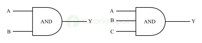
Here, A, B, and C are the input variables and Y is the output variable.
In this chapter, we will cover AND gates having three inputs only. But we can design an AND gate for any number of input variables.
Truth Table of AND Gate
The truth table of an AND gate contains inputs and outputs, and specifies the relationship between them.
The truth table of a two-input AND gate is given below −
| Input | Output | |
|---|---|---|
| A | B | Y |
| 0 | 0 | 0 |
| 0 | 1 | 0 |
| 1 | 0 | 0 |
| 1 | 1 | 1 |
From this truth table of two-input AND gate, it can be observed that the output of the AND gate is logic 1 or high, only when both inputs are logic 1 or high.
The following table represents the truth table of a three-input AND gate −
| Input | Output | ||
|---|---|---|---|
| A | B | C | Y |
| 0 | 0 | 0 | 0 |
| 0 | 0 | 1 | 0 |
| 0 | 1 | 0 | 0 |
| 0 | 1 | 1 | 0 |
| 1 | 0 | 0 | 0 |
| 1 | 0 | 1 | 0 |
| 1 | 1 | 0 | 0 |
| 1 | 1 | 1 | 1 |
This truth table shows that the output is high or logic 1 only when all the three inputs to the AND gate are high or logic 1. For rest input combinations, the output is low or logic 0.
From these truth tables of AND gate, we can conclude that an AND gate produces a high or logic 1 output, only when all its inputs are high or logic 1, otherwise the output is low or logic 0.
Working of AND Gate
The working of a two-input AND gate is explained below −
- If A = 0 and B = 0, the output is low i.e., Y = 0.
- If A = 0 and B = 1, the output is low i.e., Y = 0.
- If A = 1 and B = 0, the output is low i.e., Y = 0.
- If A = 1 and B = 1, the output is high i.e., Y = 1.
The working of a three-input AND gate is explained below −
- If A = 0, B = 0, and C = 0, the output is low i.e., Y = 0.
- If A = 0, B = 0, and C = 1, the output is low i.e., Y = 0.
- If A = 0, B = 1, and C = 0, the output is low i.e., Y = 0.
- If A = 0, B = 1, and C = 1, the output is low i.e., Y = 0.
- If A = 1, B = 0, and C = 0, the output is low i.e., Y = 0.
- If A = 1, B = 0, and C = 1, the output is low i.e., Y = 0.
- If A = 1, B = 1, and C = 0, the output is low i.e., Y = 0.
- If A = 1, B = 1, and C = 1, the output is high i.e., Y = 1.
This is all about working of a two-input and a three-input AND gates.
Boolean Expression of AND Gate
Boolean expression is a logic equation or a logic function that represents the mathematical relationship between inputs and output of the AND gate.
The Boolean expression of a two-input AND gate is given by,
Y = A · B
Where, A and B are inputs and Y is the output. This expression is read as "Y is equal to A AND B." The dot (·) symbol represents the AND operation.
For the three-input AND gate, the Boolean expression is given by,
Y = A · B · C
It is read as "Y is equal to A AND B AND C".
In the same way, we can obtain the Boolean expression for an AND gate having any number of input variables.
AND Gate using Transistor
The transistor circuit of a two-input AND gate is shown in the following figure.

The implementation of AND gate using transistors requires as many transistors as the number of inputs. For example, a two-input AND gate requires two transistors.
Working of Transistor AND Gate
The working the transistor AND gate shown in the above figure is explained below −
When both inputs A and B are low, the transistors Q1 and Q2 remain in off state and act as open switch. Therefore, the output line Y will directly connect to the ground potential. Thus, the output is low or logic 0.
When the input A is low and the input B is high, the first transistor Q1 is off and the second transistor Q2 is on. But still the supply voltage will not connect to the output line and the output line will remain at ground potential. Consequently, the output is low or logic 0.
When the input A is high and the input B is low, the transistor Q1 will conduct and the transistor Q2 will remain off. In this condition, the output line does not receive the supply voltage but connect to the ground potential. Hence, for this input combination, the output is low or logic 0.
When both inputs A and B are high, both transistors Q1 and Q2 will turn on and act as closed switches. In this condition, the supply voltage directly connect to the output line. This makes output of the circuit high or logic 1.
This is how the above transistor circuit acts a two-input AND gate. We can add more transistors to implement a high order AND gate.
AND Gate using Switches
We can also implement AND gate logic using a battery, switches, and a lamp or bulb. The following figure shows the AND gate using switches.

In this AND gate circuit, we have a voltage source, two switches representing two input terminals of the AND gate, and a lamp representing the output.
From the circuit, we see that if both switches A and B are closed, there will be a closed for current to flow in the circuit. Hence, the lamp will glow that represents the high or logic 1 output.
If both or any of the two switches be open, there will be a break in the current path, making the lamp off. This represents the low or logic 0 state of the output of the AND gate.
This way, the above depicted switching circuit performs the AND gate operation. By adding more number of switches in series, we can implement a higher order AND gate.
AND Gate IC
In practice, there is an integrated circuit namely, IC 7408 which is a most commonly used AND gate IC. This AND gate IC is implemented in transistor-transistor logic (TTL). The block diagram of the AND gate IC 7408 is shown in the following figure.

It is a Quad-2 AND gate IC having four two-input AND gates integrated on a single chip. It has 14 pins.
Conclusion
In conclusion, the AND gate is a fundamental logic gate used in digital circuits to implement the Boolean multiplication function.
The output of the AND gate is high or logic 1 only when all its inputs are high or logic 1. Otherwise, it generates a low or logic 0 output.
AND gate plays an important role in various digital electronic applications such as data processing, memory devices, arithmetic logic units, control systems, and more.
OR Gate in Digital Electronics
In digital electronics, an OR Gate is a basic logic gate having two or more input lines and one output line. It performs the Boolean addition function.
In this chapter, we will explain the theory of the OR gate. Here, we will cover the definition of OR gate, its logic symbol, Boolean expression, truth table, operation, and circuits.
So, lets get started with the basic definition of OR gate.
What is an OR Gate?
An OR gate is a type of logic gate used to perform logical addition. It can have two or more inputs and one output.
The output of the OR gate is low or logic 0 only when all its inputs are low or logic 0. For rest input combinations, the output of the OR gate is high or logic 1.
The logic symbols for a two-input and a three-input OR gate are shown in the following figure.
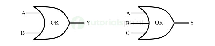
Here, A, B, and C are the input lines and Y is the output line.
Truth Table of OR Gate
The truth table is a table that shows the relationship between different input combinations and output.
The following is the truth table for a two-input OR gate −
| Input | Output | |
|---|---|---|
| A | B | Y |
| 0 | 0 | 0 |
| 0 | 1 | 1 |
| 1 | 0 | 1 |
| 1 | 1 | 1 |
The following table shows the truth table for a three-input OR gate −
| Input | Output | ||
|---|---|---|---|
| A | B | C | Y |
| 0 | 0 | 0 | 0 |
| 0 | 0 | 1 | 1 |
| 0 | 1 | 0 | 1 |
| 0 | 1 | 1 | 1 |
| 1 | 0 | 0 | 1 |
| 1 | 0 | 1 | 1 |
| 1 | 1 | 0 | 1 |
| 1 | 1 | 1 | 1 |
From these two truth tables, we can observe that the output of the OR gate is logic 0 or low, only when all the inputs to the OR gate are logic 0 or low. Otherwise, the output of the OR gate is high or logic 1.
Boolean Expression of OR Gate
The Boolean expression is a logical function that describes the mathematical relationship between inputs and output of the OR gate.
The Boolean expression of a two-input OR gate is given below −
Y = A + B
Here, A and B are input variables and Y is the output variable. This expression is read as "Y is equal to A OR B". Here, the "+" sign represents the OR operation.
Similarly, the Boolean expression of a three-input OR gate is given below −
Y = A + B + C
Here, A, B, and C are the inputs and Y is the output.
In the same way, we can extend this expression to any number of input variables.
Working of OR Gate
The operation of a two input OR gate for different input combinations is described below −
- If A = 0 and B = 0, the output of the OR gate is Y = 0.
- If A = 0 and B = 1, the output of the OR gate is Y = 1.
- If A = 1 and B = 0, the output of the OR gate is Y = 1.
- If A = 1 and B = 1, the output of the OR gate is Y = 1.
This theory explains that when both inputs applied to an OR gate are low or logic 0, the output of the OR gate is also low or logic 0, otherwise it is high or logic 1.
Similarly, the working of a three-input OR gate is described below −
- If A = 0, B = 0, and C = 0, the output of the OR gate is Y = 0.
- If A = 0, B = 0, and C = 1, the output of the OR gate is Y = 1.
- If A = 0, B = 1, and C = 0, the output of the OR gate is Y = 1.
- If A = 0, B = 1, and C = 1, the output of the OR gate is Y = 1.
- If A = 1, B = 0, and C = 0, the output of the OR gate is Y = 1.
- If A = 1, B = 0, and C = 1, the output of the OR gate is Y = 1.
- If A = 1, B = 1, and C = 0, the output of the OR gate is Y = 1.
- If A = 1, B = 1, and C = 1, the output of the OR gate is Y = 1.
This theory also explains that the output of an OR gate is low or logic 0, only when all the three inputs are low or logic 0.
OR Gate using Transistors
We can implement the OR gate logic circuit using transistors. The implementation of a two-input OR gate using BJT transistors is shown in the following figure.
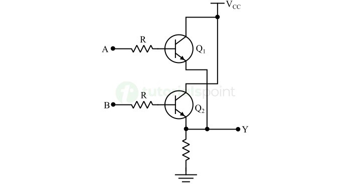
This OR gate circuit is also referred to as transistor-transistor logic (TTL) OR gate.
Working of Transistor OR Gate
The operation of the above shown transistor OR gate circuit is explained below −
When both inputs A and B are low, i.e., both A and B are connected to a low voltage (0 V), the transistors Q1 and Q2 remain off and act as open switches. The result is that the output line will directly connect to the ground potential. This makes the output of the circuit low or logic 0.
If the input A is low and the input B is high, the transistor Q1 will be off, and the transistor Q2 will turn on and acts as a closed switch. Thus, the supply voltage VCC will connect to the output line through the transistor Q2. Consequently, the output of the circuit is high or logic 1.
If the input A is high and the input B is low, the transistor Q1 will conduct, while the transistor Q2 will act as open switch. Thus, the output line will connect to the power supply VCC through the transistor Q1. Consequently, the output of the circuit is high or logic 1.
When both inputs A and B are high, both transistor Q1 and Q2 will conduct and act as the closed switches. The output line will connect to the power supply VCC through both transistors, this makes the output of the circuit high or logic 1.
This theory explains that when both inputs of the circuit are connected to logic 0 or low signal, the output is low or logic 0, otherwise the output is high or logic 1. Hence, this circuit implements the OR gate function.
We can add more transistors to the circuit to implement a higher order OR gate.
OR Gate using Switches
We can also use electrical switches, a battery, and a lamp to implement the OR logic operation. The following figure depicts the switching circuit diagram of a two-input OR gate.
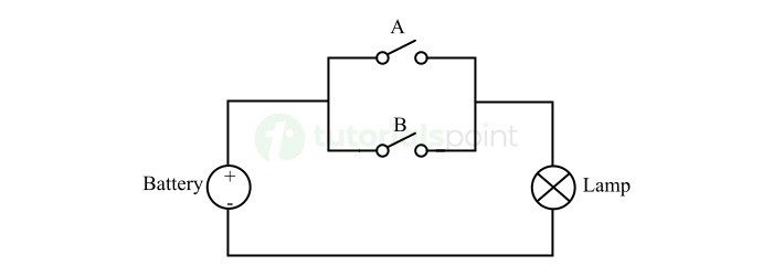
The working of this circuit is explained below −
When both switches A and B are open, there is closed path for the flow of current. Hence, the lamp will remain off which represents the low or logic 0 output.
If the switch A is open and the switch B is closed, there is a closed path for the current flow through the switch B. In this case, the lamp will glow and represents the high or logic 1 output.
If the switch A is closed and the switch B is open, there will be a closed path for the current to flow through the switch A. In this case, the lamp will glow that represents the high or logic 1 output.
If both switches A and B are closed, there will a closed path for the current to flow. This will also turn on the lamp and represents the high or logic 1 output.
This way, the above shown switching circuit implements the OR gate operation. We can add more switches in parallel to implement a higher order OR gate logic.
OR Gate IC
In practice, the OR gate is available in the form of integrated circuits or ICs. The most popular OR gate IC is IC 7432 which is a Quad 2-input OR gate IC. It has four two-input OR gates.
The following figure depicts the pin and block diagram of the OR gate IC 7432.
The OR gate IC 7432 has 14 pins and it is a transistor-transistor logic (TTL) OR gate IC.
Conclusion
In conclusion, the OR gate is a basic logic gate having two or more input lines and one output line. It produces a low or logic 0 output only when all its inputs are low, otherwise it produces a high or logic 1 output.
In this chapter, we explained the theory of OR gate. Here, we covered only two and three-input OR gates. But the same theoretical and technical explanation is valid for OR gate with any number of inputs.
NOT Gate in Digital Electronics
The NOT gate is a type of basic logic gate having only one input line and one output line. It performs the inversion operation.
In this chapter, we will explain the theory of NOT gate, its logic symbol, working, truth table, Boolean expression, etc.
In digital electronics, the NOT gate is used as the basic building block of complex digital systems.
What is a NOT Gate?
The NOT gate is a type of basic logic gate used in digital electronics to implement the inversion function. Since it performs the inversion operation, it is also known as inverter.
It has only one input line and one output line. The output of the NOT gate is high or logic 1 when its input is low or logic 0. The output of the NOT gate is low or logic 0 when its input is high or logic 1.
The logic symbol of the NOT gate is shown in the following figure −

Here, A is the input line and Y is the output line of the NOT gate.
Truth Table of NOT Gate
The truth table of NOT gate is a table of input and output that represent the relationship between them. Here is the truth table of the NOT gate −
| Input (A) | Output (Y) |
|---|---|
| 0 | 1 |
| 1 | 0 |
From this truth table, we can observe that the NOT gate inverts the input applied to it. Hence, if we apply a high input, it produces a low output and vice-versa.
Boolean Expression of NOT Gate
The Boolean expression of the NOT gate is a logical function that explains the relationship between input and output of the NOT gate mathematically.
The Boolean expression of the NOT gate is given below −
$$\mathrm{Y \: = \: \bar{A} \: = \: A'}$$
Here, the symbols "(-) overbar" and "(') prime" represents the inversion or complement operation.
This expression is read as "Y is equal to A bar or A prime or NOTed A".
Working of NOT Gate
The NOT gate performs the inversion operation of the input applied. The complete working of the NOT gate for possible input combinations is explained below −
- If A = 0, the output is Y = 1.
- If A = 1, the output is Y = 0.
Thus, the output of the NOT gate is the complement of the input applied to it.
NOT Gate using Transistor
We can implement the NOT gate logic by using a BJT transistor. When the NOT gate is implemented using a transistor, it is called a transistor inverter.
The following figure shows the circuit diagram of a NOT gate using transistor or transistor inverter.
Working of Transistor NOT Gate
The above transistor inverter circuit operates as described below −
When the input A is low, the transistor will be inactive and acts as an open switch. Thus, there is no closed path between the power supply VCC and ground terminal. Hence, the total supply voltage will appear at the output line. This represents the high or logic 1 output.
When the input A is high, the transistor will turn on and act as a closed switch. As a result, the power supply is directly connected to the ground terminal and the voltage available at the output line is equal to the ground voltage. This makes the output of the circuit low or logic 0.
This is how, the above transistor circuit implements the NOT logic.
NOT Gate using Switches
We can also implement the NOT gate operation using a battery, a switch, and a lamp. The circuit diagram for the NOT gate using switches is shown in the following figure.

In this circuit, when the switch A is open, i.e., logic 0, the current follows the path through the lamp making it glow. This represents a high or logic 1 output.
If the switch A is closed, i.e., logic 1, the current flows through the short-circuited path provided by the closed switch and no current will flow through the lamp. Hence, in this case, the lamp will be off and represents the low or logic 0 output.
From this discussion, it is clear that the output is high when the input is low and vice-versa. Thus, the above switching circuit implements the NOT gate logic.
NOT Gate IC
The NOT gate comes in the form of integrated circuits or ICs. The most commonly used NOT gate IC is IC 7404. It contains six TL (transistor logic) NOT gates.
The pin diagram of the NOT gate IC 7404 is depicted in the following figure.
Applications of NOT Gate
The NOT gate is an essential building block of various digital systems and circuits. Some key applications of NOT gate are described below −
- NOT gate is used in inverters to convert a high signal to a low signal and a low signal to a high signal.
- NOT gate is used in communication systems and storage devices.
- NOT gate is also employed as interfacing device between different logic families.
- NOT gate is also used in various digital circuits like timers, oscillators, multivibrators, modulators, etc.
Conclusion
In conclusion, the NOT gate is a logic gate used in digital electronics to implement inversion operation. It has only one input line and one output line.
The output of the NOT gate is the complement of the input signal applied to it. In this chapter, we explained the basic theory of NOT gate along with its working and applications.
Universal Gates NAND and NOR
A logic gate that can implement any kind of possible Boolean function is called a universal gate. There are two universal logic gates namely, NAND gate and NOR gate.
These two gates are called universal gates because they can perform the function of any other logic gate like AND, OR, NOT, XOR, and XNOR without need of any other type of logic gate. For example, we can perform the AND gate function by using only NAND gates or only NOR gates.
In this chapter, we will study the theory and working of the universal gates, i.e., NAND gate and NOR gate.
What is a NAND Gate?
The NAND gate is a universal gate that basically a combination of two basic logic gates namely, AND gate and NOT gate. It is designed by connecting a NOT gate to the output line of the AND gate, as shown in the following figure.

The NAND gate can have two or more input lines and one output line. The output of the NAND gate is low or logic 0 only when all its inputs are high or logic 1. Otherwise, the output of the NAND gate is high or logic 1.
The NAND gate is basically a logic gate that performs the inverse operation of an AND gate.
Being a universal gate, the NAND gate can implement any possible Boolean function or operation of any other type of logic gate.
Logic Symbol of NAND Gate
The logic symbols of a two-input and three-input NAND gates are depicted in the following figure.

Here, the bubble at the output side represents the inversion operation.
The variables A, B, and C designate the input lines and the variable Y represents the output line of the NAND gate.
Truth Table of NAND Gate
Truth table is a table of inputs and outputs of a NAND gate showing the relationship between them. Here is the truth table of a two-input NAND gate −
| Input | Output | |
|---|---|---|
| A | B | Y |
| 0 | 0 | 1 |
| 0 | 1 | 1 |
| 1 | 0 | 1 |
| 1 | 1 | 0 |
The truth table for a three-input NAND gate is given below −
| Input | Output | ||
|---|---|---|---|
| A | B | C | Y |
| 0 | 0 | 0 | 1 |
| 0 | 0 | 1 | 1 |
| 0 | 1 | 0 | 1 |
| 0 | 1 | 1 | 1 |
| 1 | 0 | 0 | 1 |
| 1 | 0 | 1 | 1 |
| 1 | 1 | 0 | 1 |
| 1 | 1 | 1 | 0 |
From these two truth tables, we can observe that the NAND gate produces a low or logic 0 output only when all its inputs are high or logic 1. For any other input combinations, the output is high or logic 1.
Boolean Expression of NAND Gate
The Boolean expression is a logical function that describes the logical relationship between inputs and output of a NAND gate.
The Boolean expression for a two-input NAND gate is give below −
$$\mathrm{Y \: = \: \overline{AB} \: = \: (AB)'}$$
The Boolean expression for a three-input NAND gate is given by,
$$\mathrm{Y \: = \: \overline{ABC} \: = \: (ABC)'}$$
Here, A, B, and C are the input variables and Y is the output variable.
Working of NAND Gate
The working of a two-input NAND gate for different input combinations is described below −
- If A = 0 and B = 0, the output of the NAND gate is Y = 1.
- If A = 0 and B = 1, the output of the NAND gate is Y = 1.
- If A = 1 and B = 0, the output of the NAND gate is Y = 1.
- If A = 1 and B = 1, the output of the NAND gate is Y = 0.
Similarly, the working of a three-input NAND gate can be explained as below −
- If A = 0, B = 0, and C = 0 the output of the NAND gate is Y = 1.
- If A = 0, B = 0, and C = 1 the output of the NAND gate is Y = 1.
- If A = 0, B = 1, and C = 0 the output of the NAND gate is Y = 1.
- If A = 0, B = 1, and C = 1 the output of the NAND gate is Y = 1.
- If A = 1, B = 0, and C = 0 the output of the NAND gate is Y = 1.
- If A = 1, B = 0, and C = 1 the output of the NAND gate is Y = 1.
- If A = 1, B = 1, and C = 0 the output of the NAND gate is Y = 1.
- If A = 1, B = 1, and C = 1 the output of the NAND gate is Y = 0.
This is all about the operation of a NAND gate for different input combinations.
It is also important to note that in this chapter, we are discussing the theory of NAND gate by considering only two and three input variables. But the same logic and theory is applicable to any number of inputs.
NAND Gate using Transistor
We can implement the NAND gate logic by using BJT transistors. Such a NAND gate is referred to as a transistor NAND gate.
The transistor circuit diagram of a two-input NAND gate is shown in the following figure.
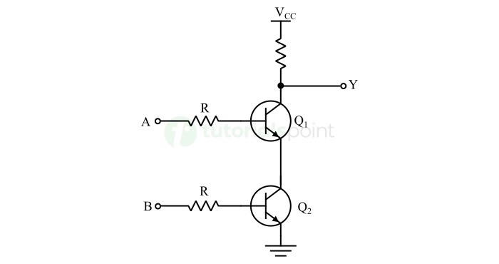
Working of Transistor NAND Gate
The working of this transistor NAND gate for different input combinations is explained below −
When both inputs A and B are connected to a low signal, the transistors Q1 and Q2 act as open switches. The entire supply voltage will appear at the output line Y. Hence, for this input combination, the output of the circuit is high or logic 1.
When the input A is at low level and the input B is at high level, the transistor Q1 acts as an open switch and the transistor Q2 acts as a closed switch. In this case, there is not a direct connection between power supply and the ground terminal. Hence, the whole supply voltage will appear at the output terminal Y, making it high or logic 1.
When the input A is at high level and the input B is at low level, the transistor Q1 acts as a closed switch and the transistor Q2 acts as an open switch. Again, there is a disconnection between power supply and the ground terminal. For this combination of inputs, the entire supply voltage will appear at the output line and sets the output high or logic 1.
When the both inputs are connected to a high or logic 1 signal, both transistors will turn on and connects the output line directly to the ground terminal i.e., to a low potential. This makes the output of the circuit low or logic 0.
Hence, the output of this circuit is low or logic 0, only when all inputs are high or logic 1, otherwise the output is high or logic 1. Thus, this circuit implements the NAND gate logic.
NAND Gate using Switches
We can also realize the NAND gate using electric switches, a battery, and a lamp. The circuit diagram of a two-input NAND gate using switches is shown in the following figure.
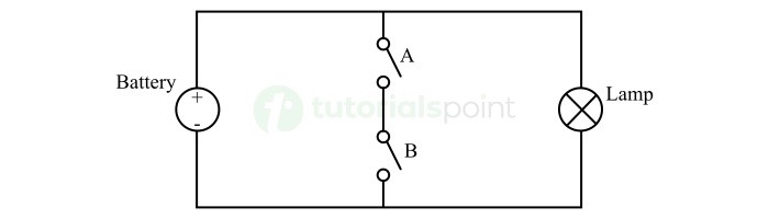
In this switching circuit, when both switches A and B are closed, there is a short-circuited path for the flow of electric current that bypasses the lamp. Hence, no current will flow through the lamp and the lamp will not glow. This represents the low or logic 0 output.
For any other switching arrangement, such as A is closed and B is open, A is open and B is closed, or A and B are open. There is no short-circuited path and the entire current will flow through the lamp, making it turn on. This represents the high or logic 1 output.
Thus, the output of this switching circuit is low or logic 0 only when both switches are closed, otherwise the output is high or logic 1. Hence, this circuit acts as a NAND gate.
We can add more switches in series with A and B to implement a higher order NAND gate.
NAND Gate as an Inverter
The NAND gate can also be used as an inverter gate. For this, all its inputs are joined together and the input signal to be inverted is applied to the common terminal as shown in the following figure.

Applications of NAND Gate
The NAND gate is used in a variety of digital and automated systems. Some of them are listed below −
- Alarm circuits
- Buzzer and burglar devices
- Automatic temperature regulation systems
- Security systems
- Automated doors and windows, etc.
This is all about the NAND gate, its working and applications. Let us now discuss the theory of another universal gate named, NOR gate.
What is a NOR Gate?
The NOR gate is another universal gate used in digital electronics to implement Boolean functions. It is a combination of two basic logic gates namely, OR gate and NOT gate. The NOR gate is designed by connecting a NOT gate to the output line and the final output is taken from the output line of the NOT gate as shown in the following figure.

Being a universal logic gate, it can be used to implement any possible Boolean function or the other logic gates single-handedly.
The NOR gate can have two or more input lines and one output line. The output of the NOR gate is high or logic 1 only when all its inputs are low or logic 0. For all other input combinations, the output of the NOR gate is low or logic 0.
Logic Symbol of NOR Gate
The logic symbols of a two-input and three-input NOR gates are shown in the following figure.
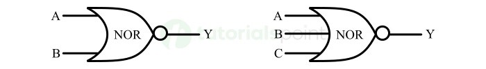
Here, A, B, and C are the input lines and Y is the output line. The bubble at the output end represents the inversion operation.
Truth Table of NOR Gate
The truth table of the NOR gate specifies the output for different input combinations. The truth table of a two-input NOR gate is given below −
| Input | Output | |
|---|---|---|
| A | B | Y |
| 0 | 0 | 1 |
| 0 | 1 | 0 |
| 1 | 0 | 0 |
| 1 | 1 | 0 |
The following is the truth table of a three-input NOR gate −
| Input | Output | ||
|---|---|---|---|
| A | B | C | Y |
| 0 | 0 | 0 | 1 |
| 0 | 0 | 1 | 0 |
| 0 | 1 | 0 | 0 |
| 0 | 1 | 1 | 0 |
| 1 | 0 | 0 | 0 |
| 1 | 0 | 1 | 0 |
| 1 | 1 | 0 | 0 |
| 1 | 1 | 1 | 0 |
From these truth tables, we can observe that the output of the NOR gate is high or logic 1 only when all its inputs are low or logic 0, otherwise the output is low or logic 0.
Working of NOR Gate
The operation of a two-input NOR gate for all possible input combinations is explained below −
- If A = 0 and B = 0, the output of the NOR gate is Y = 1.
- If A = 0 and B = 1, the output of the NOR gate is Y = 0.
- If A = 1 and B = 0, the output of the NOR gate is Y = 0.
- If A = 1 and B = 1, the output of the NOR gate is Y = 0.
Similarly, the operation of the three-input NOR gate can be described, as below −
- If A = 0, B = 0, and C = 0 the output of the NOR gate is Y = 1.
- If A = 0, B = 0, and C = 1 the output of the NOR gate is Y = 0.
- If A = 0, B = 1, and C = 0 the output of the NOR gate is Y = 0.
- If A = 0, B = 1, and C = 1 the output of the NOR gate is Y = 0.
- If A = 1, B = 0, and C = 0 the output of the NOR gate is Y = 0.
- If A = 1, B = 0, and C = 1 the output of the NOR gate is Y = 0.
- If A = 1, B = 1, and C = 0 the output of the NOR gate is Y = 0.
- If A = 1, B = 1, and C = 1 the output of the NOR gate is Y = 0.
From this discussion, we can observe that the NOR gate produces a high or logic 1 output when all its inputs are low or logic 0.
NOR Gate using Transistor
We can implement the NOR gate using transistors. The circuit diagram of a two-input NOR gate using transistors is shown in the following figure. This circuit is known as transistor NOR gate.
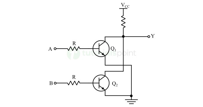
Working of Transistor NOR Gate
The working of the transistor NOR gate is explained below −
When both inputs A and B are low, the transistors Q1 and Q2 do not conduct and act as open switches. In this case, the output line Y will directly connect to the power supply. Thus, the whole supply voltage will appear at the output terminal. This makes the output of the circuit high or logic 1.
When the input A is connected to low and the input B is connected to a high signal, the transistor Q1 will act as an open switch while the transistor Q2 will act as a closed switch. In this case, the output line Y will directly connect to the ground terminal through the transistor Q2. This results in a low signal at the output line.
When the input A is connected to high and the input B is connected to a low signal, the transistor Q1 will conduct and the transistor Q2 will act as an open switch. In this case, the output line is directly connected to the ground terminal. Thus, the output is low or logic 0.
When both inputs A and B are connected to a high signal, both transistors Q1 and Q2 will act as closed switches and connect the output line directly to the ground terminal. In the case also, the output is low or logic 0.
From this discussion, we can observe that this transistor circuit implements the NOR logic and hence called as transistor NOR gate.
We can add more transistors to the circuit to obtain a higher order NOR gate.
NOR Gate using Switches
We can also realize the NOR gate using electrical switches. A circuit diagram for a two-input NOR gate using switches is shown in the following figure.
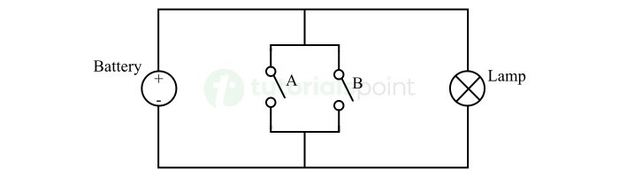
In this circuit, if both switches A and B are open, the entire current flows through the lamp and turn it on. This represents the high or logic 1 state of the output.
If both or any of the switches is closed, there is a short-circuited path for the flow of current that bypasses the lamp. In this case, the lamp will not glow and represent the low or logic 0 state of the output.
Thus, the output of this switching circuit is high or logic 1, only when both of its inputs are low i.e., open switches, otherwise the output is low or logic 0.
Therefore, this electric circuit realizes the NOR gate operation and logic.
NOR Gate as an Inverter
The NOR gate also be operated as an inverter gate. To use the NOR gate as an inverter, all its inputs are connected together and the input signal is applied to the common terminal as shown in the following figure.

Applications of NOR Gate
The NOR gate is used in numerous digital systems. Some common applications of NOR gate are listed below −
- Various digital systems
- Industrial automation and control systems
- Traffic control systems
- Alarm circuits
- Digital arithmetic circuits like adders and subtractors, etc.
Conclusion
In conclusion, a universal logic gate is one that can implement any possible Boolean functions or other logic gates without need of any other type of logic gates. In digital electronics, there are two universal logic gates namely, NAND gate and NOR gate.
In this chapter, we explained the theory, working, and applications of these two universal gates. Here, we covered only two and three-input NAND and NOR gates, but the same theory and explanation is equally valid for NAND and NOR gates with more than three inputs.
XOR Gate in Digital Electronics
In digital electronics, the XOR gate is a derived logic gate used to determine the dissimilarity between two signals.
In chapter, we will study the theory and operation of XOR gate. Lets get started with the basic definition of XOR gate.
What is an XOR Gate?
The XOR gate is a type of logic gate in digital electronics which has two inputs and one output. The output of the XOR gate is high or logic 1, only when both the inputs are different. For the same inputs, the output of the XOR gate is low or logic 0.
XOR gate is also called Exclusive OR gate or Ex-OR gate. This logic gate is widely used in digital arithmetic circuits like adders and subtractors.
Since the output of the XOR gate is high only when both of the inputs are dissimilar, it is also known as the inequality detector.
It is very important to note that there is no such thing like three or more input XOR gate. Hence, when we need XOR gate for more than two input variables, we use two or more two-input XOR gates.
Logic Symbol of XOR Gate
The logic symbol of an XOR gate is shown in the following figure.

It has only two inputs designated as A and B and one output denoted by Y.
Truth Table of XOR Gate
The truth table of XOR gate is a table that represents the relationship between its inputs and output.
The truth table of an XOR gate is given below −
| Inputs | Output | |
|---|---|---|
| A | B | Y |
| 0 | 0 | 0 |
| 0 | 1 | 1 |
| 1 | 0 | 1 |
| 1 | 1 | 0 |
From this truth table, we can observe that the output of the XOR gate is high or logic 1 only when the both inputs are different. In the case, when both inputs are similar the output is low or logic 0.
Boolean Expression of XOR Gate
The Boolean expression is a logical function that represents the relationship between inputs and output of an XOR gate mathematically.
The following equation is known as the Boolean expression of the XOR gate.
$$\mathrm{Y \: = \: A \oplus B}$$
This equation can also be expressed as below −
$$\mathrm{Y \: = \: AB' \: + \: A'B \: = \: A \bar{B} \: + \: \bar{A}B}$$
Here, the symbol "$\mathrm{\oplus}$" denotes the XOR operation.
Working of XOR Gate
The detailed working of XOR gate for different input combinations is explained below −
- If A = 0 and B = 0, the output of the XOR gate is Y = 0.
- If A = 0 and B = 1, the output of the XOR gate is Y = 1.
- If A = 1 and B = 0, the output of the XOR gate is Y = 1.
- If A = 1 and B = 1, the output of the XOR gate is Y = 0.
From this explanation, we can see the output of XOR gate is high or logic 1 only when inputs are dissimilar.
XOR Gate as an Inverter
The XOR gate can also be used as an inverter. There is a property of XOR operation that is,
$$\mathrm{A \: \oplus \: 1 \: = \: \bar{A}}$$
Hence, by utilizing this property, we can state that if one of the input lines of the XOR gate is connected to logic 1 and the input signal is applied to another input line. Then, the XOR gate produces the inverted version of the applied signal as the output.
The following figure shows the operation of XOR gate as an inverter.
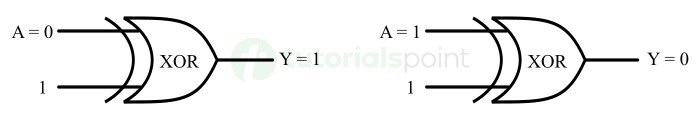
XOR Gate as a Buffer
A buffer gate is a logic gate that produces the same output as the input. It is used to provide some delay in the input and output.
There is a property of XOR logic that is,
$$\mathrm{A \: \oplus \: 0 \: = \: A}$$
Hence, if one of the two input lines of the XOR gate is connected to a logic 0 and the input signal is applied to another input line. The XOR gate then produces the output same as the input.
The operation of the XOR gate as a buffer logic is illustrated in the following figure.
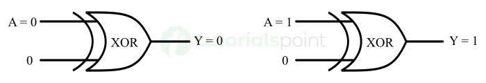
XOR Gate using Switches
We can also implement the XOR gate logic using a battery, two simple switches, and a lamp.
The following figure depicts the circuit diagram of the XOR gate using switches.
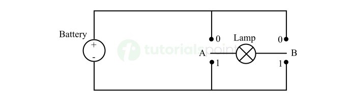
In this switching circuit, if the switches A and B are on the same level (either 0 or 1), the lamp will not glow. This state represents the low or logic 0 output.
If the switches A and B are at different levels, i.e., A is at 0 and B is at 1 or A is at 1 and B is at 0. Then, we can see there is a closed path for current to flow through the lamp, making the lamp turn on. This represents the high or logic 1 output.
Hence, the above shown electrical circuit implements the XOR logic function.
Applications of XOR Gate
The following are some key applications of the XOR gate −
- XOR gate is used in computational and arithmetic circuits like adders, subtractors, etc.
- XOR gate is used to detect errors, similarities and dissimilarities between two logic levels or signals.
- XOR gate is used as a controlled inverter or buffer logic.
Conclusion
In conclusion, the XOR gate is a two input and one output logic gate that produces a high or logic 1 output when the inputs applied to it are dissimilar.
The XOR gate logic is widely used in staircase electric wiring and many other automation circuits, where a single device like lamp has to be controlled from two different locations.
XNOR Gate in Digital Electronics
An XNOR gate is a type of derived logic gate which is a combination of an XOR gate and a NOT gate. Hence, it produces a "NOTed XOR" output.
In this chapter, we will explain the basic theory of XNOR logic gate, its working, circuit diagrams, and applications. So, lets start with the basic definition of XNOR gate.
What is XNOR Gate?
The XNOR gate is a logic gate that has two inputs and one output.
The output of the XNOR gate is high, only when both of its inputs same, i.e., either both inputs are high or both inputs are low. If the inputs are dissimilar, i.e., one is high and the other low, the output is low or logic 0.
Since the XNOR gate produces a high output when both its inputs are similar, it is also known as an equality detector.
The XNOR gate is also known as Exclusive-NOR or Ex-NOR gate.
Actually, the XNOR gate is a combination of two logic gates namely, XOR gate and NOT gate. Therefore,
XNOR Gate = XOR Gate + NOT Gate
It is important remember that there is no such thing like an XNOR gate with three or more inputs. To obtain an XNOR gate with inputs more than two, we combine multiple two-input XNOR gates together.
Logic Symbol of XNOR Gate
The logic symbol for a two input XNOR gate is shown in the following figure.

The bubble on the right-end represents the NOT operation. The variables A and B represent the input lines while Y represents the output line.
Truth Table of XNOR Gate
The truth table of an XNOR gate provides information about the operation and relationship between inputs and output of it.
The truth table of a two-input XNOR gate is given below −
| Input | Output | |
|---|---|---|
| A | B | Y |
| 0 | 0 | 1 |
| 0 | 1 | 0 |
| 1 | 0 | 0 |
| 1 | 1 | 1 |
From this truth table, it can be observed that the XNOR gate produces a high or logic 1 output when both of its inputs are same i.e., 0 and 0 or 1 and 1. Otherwise, it gives a low or logic 0 output.
Boolean Expression of XNOR Gate
The Boolean expression is a logical function that describes the relationship between inputs and output of an XNOR gate mathematically.
The Boolean expression of a two-input XNOR gate is given below −
$$\mathrm{Y \: = \: A \: \odot \: B}$$
This can also be expressed as,
$$\mathrm{Y \: = \: AB \: + \: \bar{AB}}$$
Here, A and B are input variables while Y is the output variable.
Working of XNOR Gate
The operation of a two-input XNOR gate for different input combinations is explained below −
- If A = 0 and B = 0, the output of the XNOR gate is Y = 1.
- If A = 0 and B = 1, the output of the XNOR gate is Y = 0.
- If A = 1 and B = 0, the output of the XNOR gate is Y = 0.
- If A = 1 and B = 1, the output of the XNOR gate is Y = 1.
Hence, we can see that the output is high or logic 1 for similar inputs. It is low or logic 0 for dissimilar inputs.
XNOR Gate using Switches
We can realize the XNOR gate logic with the help of two switches, a battery, and a lamp.
Here is the electrical circuit representing the XNOR logic gate.
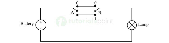
In this circuit, when both switches A and B are at same level i.e., at 0 and 0 or 1 and 1. There is a closed path for the current to flow through the lamp. This turns on the lamp and represents the high or logic 1 output.
If the switches are at different levels i.e., one is at level 0 and the other is at level 1. There is no complete path between the battery and lamp. Hence, the lamp will not glow and represent the low or logic 0 output.
Hence, the above shown switching circuit implements the XNOR logic operation.
XNOR Gate as an Inverter
The XNOR gate can operate as an inverter. If we connect one of the input lines of the XNOR gate at low or logic 0 signal and we apply the input signal to another input line. Then, the output of the XNOR gate will be the complement of the input applied.
The logic circuit of an XNOR gate working as an inverter is depicted in the following figure.

We can also explain this operation with the help of its Boolean expression as below.
$$\mathrm{Y \: = \: AB \: + \: \bar{AB}}$$
If B is set at logic 0, then
$$\mathrm{Y \: = \: A\cdot0 \: + \: \bar{A}\cdot1 \: = \: \bar{A}}$$
Hence, if one input XNOR gate is tied to logic 0, then the gate will work as an inverter.
XNOR Gate as a Buffer
The XNOR gate can also operate as a buffer. If we connect of one of the inputs of the XNOR gate to logic 1 and the input signal is applied to another input line. The output of the XNOR gate will be same as the input applied, i.e., the XNOR gate will work as a buffer.
The XNOR gate working as a buffer is shown in the following figure.

Logically, we can prove this operation through its Boolean expression as below.
$$\mathrm{Y \: = \: AB \: + \: \bar{AB}}$$
If B is set at logic 1, then
$$\mathrm{Y \: = \: A\cdot1 \: + \: \bar{A}\cdot0 \: = \: A}$$
Thus, an XNOR gate with one input set to logic 1 acts as a buffer.
Applications of XNOR Gate
The XNOR gate is widely used in numerous digital circuits and systems. Some of the key applications of XNOR gate are given below −
- XNOR gate is used in digital communication systems to detect errors that occurred during data transmission.
- XNOR gate acts as an equality detector. Thus, it is also used to compare binary data or signals.
- XNOR gate is also used to design digital gaming systems and logic puzzles.
Conclusion
In conclusion, the XNOR gate or Exclusive NOR gate is a logic gate used in various digital electronic applications. It is a two-input logic gate.
The unique functionality of the XNOR gate of equality detection is widely used in digital signal comparison and data transmission error checking.
In this chapter, we explained the basic theory and working of the XNOR gate along with its key applications.
CMOS Logic Gate in Digital Electronics
What is a Logic Gate?
In digital circuits, a logic gate is a fundamental element of the digital circuit or system, that performs a specific logical operation. A logic gates typically has one or more inputs and only one output. The output of the logic gate is related to the inputs based on a certain logic.
Some commonly used logic gates are: AND Gate, OR Gate, NOT Gate, NAND Gate, and NOR Gate.
What is CMOS Technology?
CMOS, Complementary Metal Oxide Semiconductor, is a predominant technology used for manufacturing integrated circuits (ICs). This technology is widely used for manufacturing a variety of digital electronic components like microprocessors, sensors, logic gates, and more.
CMOS technology employs both NMOS (N-Channel Metal Oxide Semiconductor) and PMOS (P-Channel Metal Oxide Semiconductor) logic to implement different types of digital functions.
CMOS technology is widely being used in realizing digital logic gates due to its key advantages, such as fast switching speed, low power consumption, high voltage range, high noise margins, etc.
Basic CMOS Logic Gates
Let us now discuss the basic CMOS logic gates in detail.
CMOS OR Gate
The OR gate is a basic logic gate in digital electronics. OR gates produce a high or logic 1 output when any of its inputs is high, and it produces a low or logic 0 output when all of its inputs are low.
The truth table of a two-input OR gate is given below.
| Input | Output | ||
|---|---|---|---|
| A | B | Y = A + B | |
| 0 | 0 | 0 | |
| 0 | 1 | 1 | |
| 1 | 0 | 1 | |
| 1 | 1 | 1 | |
The implementation of a two input OR gate in CMOS logic is shown in the following figure.
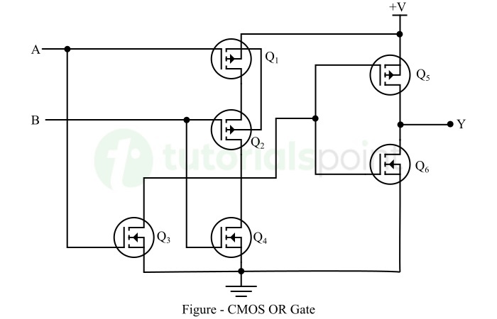
Here, we have combined multiple CMOS inverters together to build a CMOS OR gate. In the circuit diagram, the CMOS OR gate consists of a PMOS transistor and an NMOS transistor, which are joined in parallel fashion between the power supply voltage (V) and the output.
In the above circuit, when one or both inputs (A and B) are high (logic 1), the corresponding PMOS and NMOS transistors switch in a way that the current flows from the output to ground, causes a low voltage (logic 0) at the output terminal.
When both inputs are low (logic 0), the corresponding CMOS transistors switch in a way that the output is connected to the supply voltage, causing a high voltage (logic 1) at the output terminal.
CMOS AND Gate
The AND gate is a basic logic gate used in a variety of digital logic circuits. AND gate produces a high or logic 1 output only when all of its inputs are high, it produces a low or logic 0 output when any of its inputs is low.
The truth table of the two-input AND gate is given below.
| Input | Output | |
|---|---|---|
| A | B | Y = AB |
| 0 | 0 | 0 |
| 0 | 1 | 0 |
| 1 | 0 | 0 |
| 1 | 1 | 1 |
The implementation of AND gate using CMOS technology is shown in the following figure.

Here, to implement the CMOS AND gate, we have connected multiple CMOS inverters together. In the CMOS AND gate circuit, PMOS and NMOS transistors are used to build it. These transistors are connected in series between supply voltage (V) and the output (Y), and in parallel between the output and ground respectively.
In the case of CMOS AND gate shown in the above figure, when both inputs are high (logic 1), the CMOS transistors switch in such a way that the output is connected to the power supply voltage (V), producing a high (logic 1) output.
When any of its inputs is low, the CMOS transistors in the circuit switch such that the current flows from power supply to the ground, making output low (logic 0).
CMOS NOT Gate
A NOT gate is also a basic logic gate used in digital logic circuits. The NOT has a single input and a single output. The output of the NOT gate is high or logic 1 when its input is low or logic 0, and its output is low or logic 0 when its input is high or logic 1.
In CMOS logic gates, the CMOS NOT gate is the simplest CMOS logic gate. It is also called CMOS Inverter Gate.
The truth table of the NOT gate is given below.
| Input | Output |
|---|---|
| A | Y = A' |
| 0 | 1 |
| 1 | 0 |
The implementation of a NOT gate in CMOS technology is shown in the following figure.
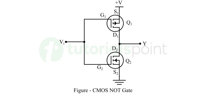
Here, the input is applied to the gate terminal of the two CMOS transistor, and the output is connected to their drain terminals.
When a positive voltage pulse (logic 1) is applied to the input Vi, the CMOS transistor Q1 is off and the CMOS transistor Q2 is on. Therefore, the output voltage will be at ground voltage, i.e. logic 0.
When the ground voltage (logic 0) is applied to the input Vi, the CMOS transistor Q1 is on and the CMOS transistor Q2 is off. Thus, the output will be closed to +V, i.e. logic 1.
Two Level Logic Realization
The maximum number of levels that are present between inputs and output is two in two level logic. That means, irrespective of total number of logic gates, the maximum number of Logic gates that are present (cascaded) between any input and output is two in two level logic. Here, the outputs of first level Logic gates are connected as inputs of second level Logic gate(s).
Consider the four Logic gates AND, OR, NAND & NOR. Since, there are 4 Logic gates, we will get 16 possible ways of realizing two level logic. Those are AND-AND, AND-OR, ANDNAND, AND-NOR, OR-AND, OR-OR, OR-NAND, OR-NOR, NAND-AND, NAND-OR, NANDNAND, NAND-NOR, NOR-AND, NOR-OR, NOR-NAND, NOR-NOR.
These two level logic realizations can be classified into the following two categories.
- Degenerative Form
- Non-degenerative Form
Degenerative Form
If the output of two level logic realization can be obtained by using single Logic gate, then it is called as degenerative form. Obviously, the number of inputs of single Logic gate increases. Due to this, the fan-in of Logic gate increases. This is an advantage of degenerative form.
Only 6 combinations of two level logic realizations out of 16 combinations come under degenerative form. Those are AND-AND, AND-NAND, OR-OR, OR-NOR, NAND-NOR, NORNAND.
In this section, let us discuss some realizations. Assume, A, B, C & D are the inputs and Y is the output in each logic realization.
AND-AND Logic
In this logic realization, AND gates are present in both levels. Below figure shows an example for AND-AND logic realization.

We will get the outputs of first level logic gates as Y1 = AB and Y2 = CD
These outputs, Y1 and Y2 are applied as inputs of AND gate that is present in second level. So, the output of this AND gate is
$$\mathrm{Y\:=\:Y_{1}Y_{2}}$$
Substitute Y1 and Y2 values in the above equation.
$$\mathrm{Y \: = \: (AB)(CD)}$$
$$\mathrm{\Rightarrow \: Y \: = \: ABCD}$$
Therefore, the output of this AND-AND logic realization is ABCD. This Boolean function can be implemented by using a 4 input AND gate. Hence, it is degenerative form.
AND-NAND Logic
In this logic realization, AND gates are present in first level and NAND gate(s) are present in second level. The following figure shows an example for AND-NAND logic realization.

Previously, we got the outputs of first level logic gates as Y1 = AB and Y2 = CD
These outputs, Y1 and Y2 are applied as inputs of NAND gate that is present in second level. So, the output of this NAND gate is
$$\mathrm{Y \: = \:(Y_{1}Y_{2})'}$$
Substitute Y1 and Y2 values in the above equation.
$$\mathrm{Y \: = \: ((AB)(CD))'}$$
$$\mathrm{\Rightarrow \: Y \: = \: (ABCD)'}$$
Therefore, the output of this AND-NAND logic realization is (ABCD)'. This Boolean function can be implemented by using a 4 input NAND gate. Hence, it is degenerative form.
OR-OR Logic
In this logic realization, OR gates are present in both levels. The following figure shows an example for OR-OR logic realization.
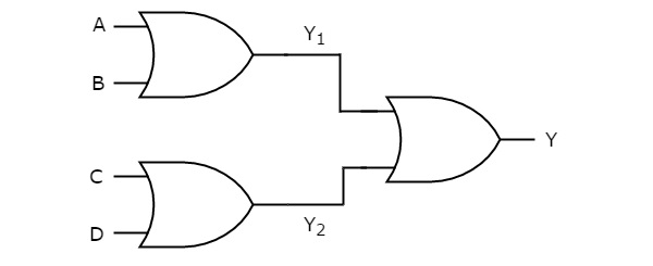
We will get the outputs of first level logic gates as Y1 = A + B and Y2 = C + D.
These outputs, Y1 and Y2 are applied as inputs of OR gate that is present in second level. So, the output of this OR gate is
$$\mathrm{Y \:= \: Y_{1}\:+\:Y_{2}}$$
Substitute Y1 and Y2 values in the above equation.
$$\mathrm{Y \: = \: (A\:+\:B) \: + \: (C\:+\:D)}$$
$$\mathrm{\Rightarrow \: Y \:=\:A\:+\:B\:+\:C\:+\:D}$$
Therefore, the output of this OR-OR logic realization is A + B + C + D. This Boolean function can be implemented by using a 4 input OR gate. Hence, it is degenerative form.
Similarly, you can verify whether the remaining realizations belong to this category or not.
Non-degenerative Form
If the output of two level logic realization can't be obtained by using single logic gate, then it is called as non-degenerative form.
The remaining 10 combinations of two level logic realizations come under nondegenerative form. Those are AND-OR, AND-NOR, OR-AND, OR-NAND, NAND-AND, NANDOR, NAND-NAND, NOR-AND, NOR-OR, NOR-NOR.
Now, let us discuss some realizations. Assume, A, B, C & D are the inputs and Y is the output in each logic realization.
AND-OR Logic
In this logic realization, AND gates are present in first level and OR gate(s) are present in second level. Below figure shows an example for AND-OR logic realization.

Previously, we got the outputs of first level logic gates as Y1 = AB and Y2 = CD.
These outputs, Y1 and Y2 are applied as inputs of OR gate that is present in second level. So, the output of this OR gate is
$$\mathrm{Y\:=\:Y_{1}\:+\:Y_{2}}$$
Substitute Y1 and Y2 values in the above equation
$$\mathrm{Y\:=\:AB\:+\:CD}$$
Therefore, the output of this AND-OR logic realization is AB + CD. This Boolean function is in Sum of Products form. Since, we cant implement it by using single logic gate, this AND-OR logic realization is a non-degenerative form.
AND-NOR Logic
In this logic realization, AND gates are present in first level and NOR gate(s) are present in second level. The following figure shows an example for AND-NOR logic realization.
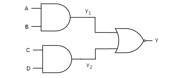
We know the outputs of first level logic gates as Y1 = AB and Y2 = CD
These outputs, Y1 and Y2 are applied as inputs of NOR gate that is present in second level. So, the output of this NOR gate is
$$\mathrm{Y \:=\:(Y_{1}\:+\:Y_{2})'}$$
Substitute Y1 and Y2 values in the above equation.
$$\mathrm{Y\:=\:(AB\:+\:CD)'}$$
Therefore, the output of this AND-NOR logic realization is (AB + CD)'. This Boolean function is in AND-OR-Invert form. Since, we cant implement it by using single logic gate, this AND-NOR logic realization is a non-degenerative form
OR-AND Logic
In this logic realization, OR gates are present in first level & AND gate(s) are present in second level. The following figure shows an example for OR-AND logic realization.
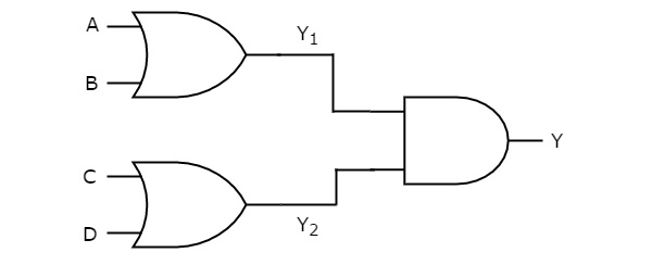
Previously, we got the outputs of first level logic gates as Y1 = A + B and Y2 = C + D.
These outputs, Y1 and Y2 are applied as inputs of AND gate that is present in second level. So, the output of this AND gate is
$$\mathrm{Y\:=\:Y_{1}Y_{2}}$$
Substitute Y1 and Y2 values in the above equation.
$$\mathrm{Y \: = \: (A\:+\:B)(C\:+\:D)}$$
Therefore, the output of this OR-AND logic realization is (A + B) (C + D). This Boolean function is in Product of Sums form. Since, we cant implement it by using single logic gate, this OR-AND logic realization is a non-degenerative form.
Similarly, you can verify whether the remaining realizations belong to this category or not.
Digital Electronics - Threshold Logic
In previous chapters, we have implemented various combinational circuits using logic gates. Except NOT gate, the remaining all logic gates have at least two inputs and single output. Similarly, the threshold gate also contains at least one input and only one output.
Additionally, it contains the respective weights to each input and a threshold value. The values of these weights and threshold could be of any finite real number.
Basics of Threshold gate
Let the inputs of threshold gate are X1, X2,X3,, Xn. The corresponding weights of these inputs are W1, W2,W3, , Wn. The symbol of Threshold gate is shown in the following figure.

Threshold gate is represented with a circle and it is having 'n' inputs, X1 to Xn and single output, Y. This circle is made into two parts. One part represents the weights corresponding to the inputs and other part represents Threshold value, T.
The sum of products of inputs with corresponding weights is known as weighted sum. If this weighted sum is greater than or equal to Threshold value, T then only the output, Y will be equal to one. Otherwise, the output, Y will be equal to zero.
Mathematically, we can write this relationship between inputs and output of Threshold gate as below.
$$\mathrm{Y \: = \: 1 \:\: if \: \: W_{1}X_{1} \: + \: W_{2}X_{2} \: + \: W_{3}X_{3} \: + \: \dotso \: + \: W_{n}X_{n} \: \geq \: T}$$
= 0, otherwise.
Therefore, we can implement various logic gates and Boolean functions just by changing the values of weights and / or Threshold value, T.
Example
Let us find the simplified Boolean function for the following Threshold gate.

This Threshold gate is having three inputs X1, X2, X3 and one output Y.
The weights corresponding to the inputs X1, X2 & X3 are W1 = 2, W2 = 1 & W3 = -4 respectively.
The value of Threshold gate is T = -1.
The weighted sum of Threshold gate is
$$\mathrm{W \: = \: W_{1}X_{1} \: + \: W_{2}X_{2} \: + \: W_{3}X_{3}}$$
Substitute the given weights in the above equation.
$$\mathrm{\Rightarrow \: W \: = \: 2X_{1} \: + \: X_{2} \: − \: 4X_{3}}$$
Output of Threshold gate, Y will be '1' if W ≥ 1, otherwise it will be '0'.
The following table shows the relationship between the input and output for all possible combination of inputs.
| Input | Weighted Sum | Output | ||
|---|---|---|---|---|
| X1 | X2 | X3 | W = 2X1 + X2 - 4X3 | Y |
| 0 | 0 | 0 | 0 | 1 |
| 0 | 0 | 1 | -4 | 0 |
| 0 | 1 | 0 | 1 | 1 |
| 0 | 1 | 1 | -3 | 0 |
| 1 | 0 | 0 | 2 | 1 |
| 1 | 0 | 1 | -2 | 0 |
| 1 | 1 | 0 | 3 | 1 |
| 1 | 1 | 1 | -1 | 1 |
From the above table, we can write the Boolean function for output, Y as
$$\mathrm{Y \: = \: \sum m( 0,2,4,6,7)}$$
The simplification of this Boolean function using 3 variable K-Map is shown in the following figure.
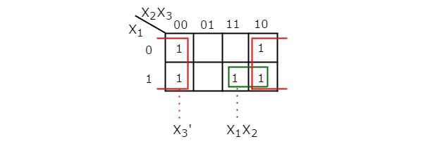
Therefore, the simplified Boolean function for given Threshold gate is Y = X3' + X1 X2.
Synthesis of Threshold Functions
Threshold gate is also called as universal gate because we can implement any Boolean function using Threshold gate(s). Some-times, it may not possible to implement few logic gates and Boolean functions by using single Threshold gate. In that case, we may require multiple Threshold gates.
Follow these steps for implementing a Boolean function using single Threshold gate.
Step 1 − Formulate a Truth table for given Boolean function.
Step 2 − In the above Truth table, add (include) one more column, which gives the relation between weighted sums and Threshold value.
Step 3 − Write the relation between weighted sums and threshold for each combination of inputs as mentioned below.
- If the output of Boolean function is 1, then the weighted sum will be greater than or equal to Threshold value for those combination of inputs.
- If the output of Boolean function is 0, then the weighted sum will be less than Threshold value for those combination of inputs.
Step 4 − Choose the values of weights & Threshold in such a way that they should satisfy all the relations present in last column of the above table.
Step 5 − Draw the symbol of Threshold gate with those weights and Threshold value.
Example
Let us implement the following Boolean function using single Threshold gate.
$$\mathrm{Y( X_{1},X_{2},X_{3})\:=\: \sum m ( 0,2,4,6,7)}$$
The given Boolean function is a three variable function, which is represented in sum of min terms form. The Truth table of this function is shown below.
| Input | Output | ||
|---|---|---|---|
| X1 | X2 | X3 | Y |
| 0 | 0 | 0 | 1 |
| 0 | 0 | 1 | 0 |
| 0 | 1 | 0 | 1 |
| 0 | 1 | 1 | 0 |
| 1 | 0 | 0 | 1 |
| 1 | 0 | 1 | 0 |
| 1 | 1 | 0 | 1 |
| 1 | 1 | 1 | 1 |
Now, let us add (include) one more column to the above Truth table. This last column contains the relations between weighted sums (W) and Threshold value (T) for each combination of inputs.
| Input | Output | Relations Between W & T | ||
|---|---|---|---|---|
| X1 | X2 | X3 | Y | |
| 0 | 0 | 0 | 1 | $\mathrm{0 \: \geq \: T}$ |
| 0 | 0 | 1 | 0 | $\mathrm{W_{3} \: \lt \: T}$ |
| 0 | 1 | 0 | 1 | $\mathrm{W_{2} \: \geq \: T}$ |
| 0 | 1 | 1 | 0 | $\mathrm{W_{2}+W_{3} \: \lt \: T}$ |
| 1 | 0 | 0 | 1 | $\mathrm{W_{1} \: \geq \: T}$ |
| 1 | 0 | 1 | 0 | $\mathrm{W_{1}+W_{3} \: \lt \: T}$ |
| 1 | 1 | 0 | 1 | $\mathrm{W_{1}+W_{2} \: \geq \: T}$ |
| 1 | 1 | 1 | 1 | $\mathrm{W_{1}+W_{2}+W_{3} \: \geq \: T}$ |
Following are the conclusions from the above table.
- The value of Threshold should be either zero or negative based on first relation.
- The value of W3 should be negative based on first and second relations.
- The values of W1 and W2 should be greater than or equal Threshold value based on fifth and third relations.
- W2 should be greater than W3 based on fourth relation.
We can choose the following values for weights and Threshold based on the above conclusions.
W1 = 2, W2 = 1, W3 = -4 & T = -1
The symbol of Threshold gate with the above values is shown below.
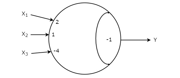
Therefore, this Threshold gate implements the given Boolean function, $\mathrm{Y( X_{1}, X_{2},X_{3}) \:=\: \sum m (0,2,4,6,7)}$.
Digital Electronics - Boolean Algebra
Boolean algebra is a branch of mathematics that provides a set of operations and rules to manipulate and process binary variables. It is considered the foundation of digital electronics and computer science.
Boolean algebra is based on the binary number system. In this chapter, we will cover the basic theory of Boolean algebra, its significance, advantages, limitations, and applications.
What is Boolean Algebra?
Boolean algebra is a mathematics that provides various operators and rules to perform arithmetic and algebraic operations on binary variables and numbers. The Boolean algebra is based on the binary number system and logical arithmetic. Thus, it is also referred to as logical algebra.
Boolean algebra was developed by a mathematician and logician George Boole in the year of 1847.
Today, Boolean algebra is being used as the fundamental of digital electronics, computer systems, and information technology.
Since, Boolean algebra is based on the binary number system. Hence, the Boolean variables can take only two possible values i.e., 0 and 1. Here, the value 0 represents the False state, while the value 1 represents the True state.
The operations in Boolean algebra are based on the three fundamental logical operations namely, AND, OR, and NOT.
Let us discuss about each of these three logical operations in detail.
Logical Operations in Boolean Algebra
The following are the fundamental logical operations that form the basis of Boolean algebra −
AND Operation
In Boolean algebra, a logical operation in which the outcome is true (1) only when all the input values are true (1), otherwise, the output is false (0) is termed as AND operation. The AND operation is represented by a dot (.). For example, A AND B can be represented as A.B in symbolic form.
OR Operation
In Boolean algebra, the OR operation is another logical operation in which the output is false (0) only when all input values are false (0), otherwise the output is true (1). The OR operations is denoted by a plus (+). For example, A OR B can be represented as A + B.
NOT Operation
In Boolean algebra, the NOT operation is performed to obtain the inverted version of the input value. Thus, the result of the NOT operation is false (0), if the input is true (1) and vice-versa. The NOT operation is represented by the symbol "~". For example, NOT A is represented as ~A.
These are the basic operations used in the Boolean algebra. However, there are many more logical operations and rules that used in the Boolean algebra to perform complex tasks.
Terminology of Boolean Algebra
The following are some important terms commonly used in Boolean algebra −
Boolean Variable
A Boolean variable is a symbol that can take one of the two possible binary values i.e., 0 and 1.
Boolean Value
It is nothing but a value representing the state of a variable. It can be either True (1) or False (0).
Boolean Function or Expression
It is a logical expression that consists of Boolean variables and values, and logical operators like AND, OR, or NOT. It represents a logical relationship between all the elements.
Logic Gate
A logic gate is a digital circuit that can perform a specific logical operation. There are 7 main logic gates used in digital electronics, they are AND gate, OR gate, NOT gate, NOR gate, NAND gate, XOR gate, and XNOR gate.
These are the basic terms used in Boolean algebra and provides a foundation for its understanding and working.
Significance of Boolean Algebra in Digital Electronics
Boolean algebra plays a crucial role in building the foundation of the digital electronics and computer science.
Here is a list of some of key factors that make Boolean algebra an important concept in the field of digital electronics −
- Boolean algebra utilizes binary number system that provides a simplified way of representing on and off states of a digital system. Where, 0 is used to denote the off state, while 1 is used to represent the on state of the system.
- Boolean algebra provides various efficient methods like K-map, QC method, etc. to simplify complex logical operations.
- Boolean algebra allows to implement various arithmetic and logical operations using simple logic gates.
- Boolean algebra enables us to develop switching algorithms that are essential components in various computer networks and communication systems.
- Boolean algebra provides various rules and sets of operations used in computer programming to perform logical and decision-making operations.
- Boolean algebra simplifies the data storage and transmission processes.
- Boolean algebra provides a foundation for developing artificial intelligence and machine learning technologies.
Overall, the Boolean algebra creates a fundamental structure and framework to develop and implement various digital electronic systems and information-based technologies. Hence, it is an important concept in the field of digital electronics.
Advantages of Boolean Algebra
Boolean algebra has numerous advantages in the field of digital electronics. Some key benefits of Boolean algebra are listed below −
- Boolean algebra provides a rich set of laws and theorems to simplify complex logical functions so that they can implemented using a smaller number of digital components. This simplification makes the digital circuits significantly cost-effective, simpler to design and implement, and low power consuming.
- Boolean algebra provides various tools to analyze and verify the functionality of digital systems to meet the desired requirements.
- The operations based on Boolean algebra can be analyzed and simulated using digital tools and software.
- Boolean algebra provides the logical foundation for programming and software development.
- Boolean algebra enables us to create, analyze, and simulate the real-world systems.
- Boolean algebra helps understand the working and logical implementation of digital circuits, systems, and software.
Hence, all these advantages of Boolean algebra make it a perfect foundation for understanding, analyzing, and designing the digital systems.
Disadvantages of Boolean Algebra
Boolean algebra is a powerful tool in terms of design and analysis of digital systems. But it also has some disadvantages.
Here is a list of some of the major disadvantages of Boolean algebra −
- Boolean algebra is based on the binary number system and is best suited for digital systems. It cannot be used in the applications where continuous representation of information is desired.
- Boolean algebra is based on the true or false statements. Hence, it is not suitable for quantitative representation of information.
- Boolean algebra has a limited set of logical operations like AND, OR, and NOT.
- Boolean algebra becomes complex to manage in the case of large digital systems due to a greater number of variables.
- Boolean algebra does not provide any mean to directly represent the arithmetic operations such as addition, subtraction, multiplication, and division.
- Boolean algebra cannot represent the analog signals or continuous functions.
- Boolean algebra does not support various advanced mathematical concepts which are required in numerous engineering and scientific applications.
Although it has some disadvantages, Boolean algebra still forms the foundation of digital electronics and computer science.
Applications of Boolean Algebra
Boolean algebra is a fundamental tool used in a wide range of applications in the field of digital electronics. Some of the key applications of Boolean algebra are listed below −
- Boolean algebra is used to design digital circuits and systems.
- Boolean algebra is used to simplify and optimize the implementation and operation of digital circuits.
- Boolean algebra is used to develop logical concepts and control structures in computer programming and software development environment.
- Boolean algebra plays a vital role in the design and operation of central processing unit or CPU of a computing system.
- Boolean algebra also important in the field of internet and operations of search engines. It helps filtering the search queries to provide accurate results.
- Telecommunication systems also utilize the Boolean algebra for data routing, data communication, error detection and correction purposes.
- Boolean algebra plays a crucial role in optimization of computer networks and their operation.
- Boolean algebra is also used to design control systems for automate the processes in the field of robotics and industrial automation.
These are some common examples of applications of Boolean algebra. Although, this list can extend to any number because Boolean algebra is the foundation of digital systems and computer science.
Conclusion
In conclusion, Boolean algebra is a mathematics of logic that provides a set of rules and a framework to design and develop digital and logical systems.
Boolean algebra is basically a tool developed to design, analyze, and optimize the digital circuits and systems. It helps simplify the design and implementation of digital circuits.
Boolean algebra is an important concept in the field of digital electronics, computer programming, internet, databases, digital communication, artificial intelligence, etc.
The key feature of Boolean algebra is that it can represent information in the binary form that can be processed using digital systems and computers.
In this chapter, we explained the basics of Boolean algebra. In the next chapter, we will learn the laws and rules of Boolean algebra.
Laws of Boolean Algebra
Boolean algebra is a mathematical tool that deals with logical operations and binary number system. It builds the foundation of digital electronics and computer science.
The laws and rules in Boolean algebra are the sets of logical statements or expressions upon which all the logical expressions are built. Each law of the Boolean algebra can be interpreted as an operation performed by a logic circuit like a logic gate.
In this chapter, we will learn about laws and rules of Boolean algebra that are used to simplify the logical functions and Boolean expressions. These laws and rules are essential tools in Boolean algebra that help to reduce the complexity and optimize the digital circuits and systems.
Let us learn the primary laws and rules of Boolean algebra in detail that are used to perform logical operations.
Laws of Boolean Algebra
All the important laws and rules of Boolean algebra are explained below −
Rules of Logical Operations
There are three basic logical operations namely, AND, OR, and NOT. The following table highlights the rules associated with these three logical operations −
| AND Operation | OR Operation | NOT Operation |
|---|---|---|
| 0 AND 0 = 0 | 0 OR 0 = 0 | NOT of 0 = 1 |
| 0 AND 1 = 0 | 0 OR 1 = 1 | NOT of 1 = 0 |
| 1 AND 0 = 0 | 1 OR 0 = 1 | |
| 1 AND 1 = 1 | 1 OR 1 = 1 |
These rules of Boolean algebra can be implemented using logic gates.
AND Laws
In Boolean algebra, there are four AND laws given below −
- Law 1 − A · 0 = 0 (This law is called null law).
- Law 2 − A · 1 = A (This law is called identity law).
- Law 3 − A · A = A
- Law 4 − A · A' = 0
OR Laws
There are four OR laws described below −
- Law 1 − A + 0 = A (This law is called null law).
- Law 2 − A + 1 = 1 (This law is called identity law).
- Law 3 − A + A = A
- Law 4 − A + A' = 1
Complementation Laws
There are following five complementation laws in Boolean algebra −
- Law 1 − 0' = 1
- Law 2 − 1' = 0
- Law 3 − If A = 0, Then A' = 1
- Law 4 − If A = 1, Then A' = 0
- Law 5 − (A')' = A (This is called double complementation law)
Commutative Laws
There are following two commutative laws in Boolean algebra −
Law 1 − According to this law, the operation A OR B produces the same output as the operation B OR A, i.e.,
A + B = B + A
Hence, the order of the variables does not affect the OR operation.
This law can be extended to any number of variables. For example, for three variables, it will be,
A + B + C = C + B + A = B + C + A = C + A + B
Law 2 − According to this law, the output of the A AND B operation is same as that of the B AND A operation, i.e.,
A · B = B · A
This law states that the order in which the variables are ANDed does not affect the result.
We can extend this law to any number of variables. For example, for three variables, we get,
A · B · C = A · C · B = C · B · A = C · A · B
Associative Laws
Associative laws define the ways of grouping the variables. There are two associative laws as described below.
Law 1 − The expression A OR B ORed with C results the same as the A Ored with B OR C, i.e.,
(A + B) + C = A + (B + C)
This law can be extended to any number of variables. For example, for 4 variables, we get,
(A + B + C) + D = A + (B + C + D) = (A + B) + (C + D)
Law 2 − The expression A AND B ANDed with C results the same as the expression A ANDed with B AND C, i.e.,
(A · B) · C = A · (B · C)
We can extend this law to any number of variables. For example, if we have 4 variables, then
(ABC)D = A(BCD) = (AB)·(CD)
Distributive Laws
In Boolean algebra, there are the following two distributive laws that allow for multiplying or factoring out of expressions.
Law 1 − According to this law, we OR several variables and then AND the result with a single variable.
It gives the same result as the expression in which the single variable is ANDed with each of the several variables and then ORed the product terms, i.e.,
A · (B + C) = AB + AC
We can extend this law to any number of variables. For example,
A(BC + DE) = ABC + ADE
AB(CD + EF) = ABCD + ABEF
Law 2 − According to this law, if we AND several variables and then the result is ORed with a single variable.
It gives the same result as we OR the single variable with each of the several variables and then the sum terms are ANDed together, i.e.,
A + BC = (A + B)(A + C)
Proof − The proof of this law is explained here,
RHS = (A + B)(A + C)
= AA + AB + AC + BC
= A + AB + AC + BC
= A (1 + B + C) + BC
Since,
1 + B + C = 1 + C = 1
Therefore,
A · 1 + BC = A + BC = LHS
Redundant Literal Rule (RLR)
Under this rule, there are two laws in Boolean algebra, which are explained here.
Law 1 − According to this law, if we OR a variable with the AND of the complement of the variable and another variable. Then, it is same as the OR of the two variables, i.e.,
A + AB = A + B
Proof − The proof of this law is explained here,
LHS = A + AB = (A + A)(A + B)
= 1 · (A + B) = A + B = RHS
Law 2 − According to this law, if we AND a variable with the OR of the complement of the variable and another variable, it is equivalent to when we AND the two variables, i.e.,
A(A + B) = AB
Proof − This law can be proved as follows,
LHS = A(A + B) = AA + AB
= 0 + AB = AB = RHS
Both these laws show that the complement of a term appearing in another term is redundant. Hence, the rule is named as Redundant Literal Rule.
Idempotence Laws
The term "idempotence" is a synonym for "same value". There are two idempotence laws in Boolean algebra. They are,
Law 1 − According to this law, ANDing a variable with itself is equal to the variable, i.e.,
A · A = A
Law 2 − According to this law, ORing a variable with itself is equal to the variable, i.e.,
A + A = A
Absorption Laws
There are two absorption laws in Boolean algebra and they are explained below.
Law 1 − According to this law, if we OR a variable with the AND of the that variable and another variable, then it is equal to the variable itself, i.e.,
A + A · B = A
This can be proved as follows,
LHS = A + A · B = A · (1 + B)
= A · 1 = A = RHS
Law 2 − According to this law, the AND of a variable with the OR of that variable and another variable is equivalent to the variable itself i.e.,
A(A + B) = A
This can also be proved as follows,
LHS = A(A + B) = AA + AB
= A + AB = A(1 + B) = A · 1 = A = RHS
Hence, this law proves that if a term appears in another term, then the latter term will become redundant and can be removed from the expression.
DeMorgan's Theorem
In Boolean algebra, DeMorgans theorem defines two laws which are explained below.
Law 1 − According to this law, the complement of a sum of variables is equivalent to the product of complement of each of the variables, i.e.,
$$\mathrm{\overline{A+B} \: = \: \bar{A}\cdot\bar{B}}$$
This law can be extended to any number of variables.
Law 2 − The second law of DeMorgans theorem states that the complement of a product of variables is equivalent to the sum of complement of each of the variables, i.e.,
$$\mathrm{\overline{AB} \: = \: \bar{A}\: + \:\bar{B}}$$
This law can also be extended to any number of variables.
Conclusion
In this chapter, we explained all the important laws, rules, and theorems used in Boolean algebra. These rules and laws are extensively used to simplify the logical expressions in digital electronics.
Basically, all these rules provide a set of tools for simplification of complex Boolean functions and make the digital circuits simpler.
Digital Electronics - Boolean Functions
In digital electronics, boolean function is a fundamental concept that defines the logical and mathematical relationship between input binary variables and binary result. These functions are defined as per the rules of Boolean algebra and binary number system.
In this chapter, we will explain the fundamentals of Boolean functions, their properties, advantages, applications. So, lets get started with a basic introduction to Boolean function.
What is a Boolean Function?
A Boolean function is a mathematical expression consists of binary variables and logical operators. It defines a logical relationship between the binary variables and binary output.
The Boolean functions are defined using the rules of Boolean algebra and binary number system. These functions build the foundation of design and development of digital circuits and systems.
Components of a Boolean Function
A Boolean function consists of the following two major components −
- Binary Variables
- Logical Operators
Binary Variables
A binary variable is a symbol that can take one of the two possible values i.e., 0 and 1. If a binary variable has a value 0 associated to it. Then, it represents a low or false state. While if the value of the binary variable is 1, then it represents the high or true state.
Logical Operators
A logical operator is a symbol that represents a logical operation or process. In Boolean algebra, there are three basic logical operators −
AND Operator
It is denoted by a dot (.). The output of the AND operation is true or high or logic 1, if and only if all its input variables have a value true or high or logic 1. It is a binary operator, as it requires minimum two input variables.
OR Operator
It is denoted by a plus sign (+). It is also a binary operator, as minimum two input variables are required. The output of the OR operation is true or high or logic 1, if any of its inputs is true or high or logic 1.
NOT Operator
The NOT operator is represented by the symbol tilde (~). It is a unary operator requires only one input variable. The NOT operator inverts or complements the value of the input variable. Thus, if the value of the input variable is 1, it gives 0 as output and vice versa.
Representations of Boolean Functions
A Boolean function can be represented in several different forms. The following are some commonly used representations of Boolean functions −
Mathematical Form
In this form, the Boolean expression is represented as a mathematical expression consisting of binary variables and logical operators in their symbol form. For example,
Y(A,B,C) = AB + ABC + BC
This form is also known as algebraic form.
Truth Table
In this form, a Boolean function is represented in a tabular format. The table represents all the possible combinations of binary variables and their corresponding binary outputs of the Boolean function.
For example, Y = A + B is a Boolean function and its truth table representation is shown below.
| A | B | Y |
|---|---|---|
| 0 | 0 | 0 |
| 0 | 1 | 1 |
| 1 | 0 | 1 |
| 1 | 1 | 1 |
Logic Circuit Diagram
It is the graphical representation of a Boolean function. The logic circuit diagram represents a Boolean function through an interconnection of logic gates. Where, each logic gate is represented by using its symbol.
The logic circuit diagram of a Boolean function Y = AB + AC is shown in the following figure.

Importance of Boolean Function in Digital Electronics
In digital electronics, Boolean function is the key concept used to express a logical relation between different variables and output values. As we know, digital systems work with binary information, where the binary information is expressed using binary variables.
Boolean functions provide an efficient and logical way of expressing the relationship between these binary variables, so that the system can understand and manipulate the binary information.
Boolean functions also provide a basis for designing of logic gates and other digital circuits. Basically, they provide a systematic and mathematical approach to design and analyze digital systems.
We can also use Boolean functions to understand and verify the behavior of the digital circuits for different possible inputs. Therefore, Boolean functions are also utilized as the debugging and optimization tools for digital systems.
Overall, Boolean function is a standardized tool used in the field of digital electronics to perform various tasks, such as implementation, analysis, optimization, and verification of operation of digital circuits and systems.
Characteristics of Boolean Functions
A Boolean function has several important characteristics that makes it a crucial tool for designing, implementing, and analyzing digital circuits. Some of the key characteristics of Boolean functions are listed below −
- Boolean functions provide a simple and clear method to express a logical relationship between input variables and output of a digital system.
- A Boolean function can be used as an instrument to understand the behavior of a digital circuit for different input combinations.
- Boolean functions are composed of binary variables. Hence, they can be directly realized using logic gates.
- Boolean functions also help determining the output of digital systems without their actual implementation.
- Boolean functions also play a crucial role in reducing system complexity and cost minimization.
- Boolean functions allow to detect and correct the errors in digital system design to improve the accuracy and reliability.
All these are the important characteristics of Boolean function. Apart from these advantages, Boolean functions also have several limitations, which are listed in the next section.
Limitations of Boolean Functions
Here is a list of some of key limitations of Boolean functions −
- Boolean functions are dependent on binary number system. Hence, they are not suitable to represent many problems outside the field of digital electronics.
- Boolean functions are very sensitive to small variations in the input values. This high sensitivity can sometimes produce unpredictable results.
- Boolean functions cannot express the natural arithmetic operations directly.
- Boolean functions are not convenient for some applications like statistical modeling.
Applications of Boolean Functions
Boolean functions have a wide range of applications in the field of digital electronics and computer science.
Some of key applications of Boolean functions are described below −
- Boolean functions are used to design, analyze, and implement the digital circuits.
- The design and operation of computer systems and microprocessors is defined through the Boolean functions.
- Boolean functions are also used to express the outputs of the logic gates, flip-flops, counters, decoders, and all the other digital systems.
- Boolean functions are also used to design the circuits employed for digital signal processing.
- Boolean functions are used in electrical and electronics engineering to design, implement, and analyse the control systems, automation systems, etc.
Conclusion
In conclusion, a Boolean function is an elementary tool used to specify a systematic, mathematical, and logical relationship between binary variables and the output of a digital system.
Boolean functions are so versatile that they can be used for various purposes such as designing, analysis, implementation, optimization, etc. of the digital systems.
Digital Electronics - DeMorgan's Theorem
In Boolean algebra, several rules are defined to perform operations in digital logic circuits. Boolean algebra is a tool to perform operation on binary digits, i.e. 0 and 1. These two binary digits 0 and 1 are used to denote FALSE and TRUE states of a digital circuit at input and output ends. Boolean algebra, developed by George Boole, uses 0s and 1s to create truth tables and logic expressions of digital circuits like AND, OR, NOT, etc. which are used to analyze and simplify the complex circuits.
There were another English mathematician Augustus DeMorgan who explained the NAND and NOR operations as NOT AND and NOT OR operations respectively. This explanation was named De Morgan's Theorem. In this tutorial, we will discuss the DeMorgan's theorem in detail.
What is DeMorgan's Theorem?
DeMorgan's Theorem is a powerful theorem in Boolean algebra which has a set of two rules or laws. These two laws were developed to show the relationship between two variable AND, OR, and NOT operations. These two rules enable the variables to be negated, i.e. opposite of their original form. Therefore, DeMorgan's theorem gives the dual of a logic function.
Now, let us discuss the two laws of DeMorgan's theorem.
DeMorgan's First Theorem (Law 1)
DeMorgan's First Law states that the complement of a sum (ORing) of variables is equal to the product (ANDing) of their individual complements. In other words, the complement of two or more ORed variables is equivalent to the AND of the complements of each of the individual variables, i.e.
$$\mathrm{\overline{A+B} \: = \: \bar{A} \cdot \bar{B}}$$
Or, it may also be represented as,
$$\mathrm{\lgroup A \: + \: B \rgroup' \: = \: A'\cdot B'}$$
The logic implementation of left side and right side of this law is shown in Figure 1.

Thus, DeMorgan's first law proves that the NOR gate is equivalent to a bubbled AND gate. The following truth table shows the proof of this law.
| Left Side | Right Side | ||||
|---|---|---|---|---|---|
| Input | Output | Input | Output | ||
| A | B | (A + B)' | A' | B' | A'· B' |
| 0 | 0 | 1 | 1 | 1 | 1 |
| 0 | 1 | 0 | 1 | 0 | 0 |
| 1 | 0 | 0 | 0 | 1 | 0 |
| 1 | 1 | 0 | 0 | 0 | 0 |
This truth table proves that the Boolean expression on the left is equivalent to that on the right side of the expression of DeMorgan's first law.
Also, the first law of DeMorgan's theorem can be extended to any number of variables, or a combination of variables.
For example,
$$\mathrm{\overline{A \: + \: B \: + \: C \: + \: D \: + \: E \: + \: \dotso} \: = \: \bar{A} \: \bar{B} \: \bar{C} \: \bar{D} \: \bar{E} \: \dotso}$$
Also,
$$\mathrm{\overline{ABC \: + \: DE \: + \: FGH \: + \: \dotso}\: = \: \overline{\lgroup ABC \rgroup}.\overline{\lgroup DE \rgroup}.\overline{\lgroup FGH\rgroup}.\dotso}$$
From the above discussion, we may conclude that the DeMorgan's First Law converts an expression from a sum form under a NOT sign to a product form.
DeMorgan's Second Theorem (Law 2)
DeMorgan's second law states that the complement of the product (ANDing) of variables is equivalent to the sum (ORing) of their individual complements.
In other words, the complement of two or more ANDed variables is equal to the sum of the complement of each of the individual variables, i.e.,
$$\mathrm{\overline{AB} \: = \: \overline{A} \: + \: \overline{B}}$$
It may also be represented as,
$$\mathrm{\lgroup AB \rgroup' \: = \: A' \: + \: B'}$$
The logic implementation of left and right sides of this expression is shown in Figure 2.
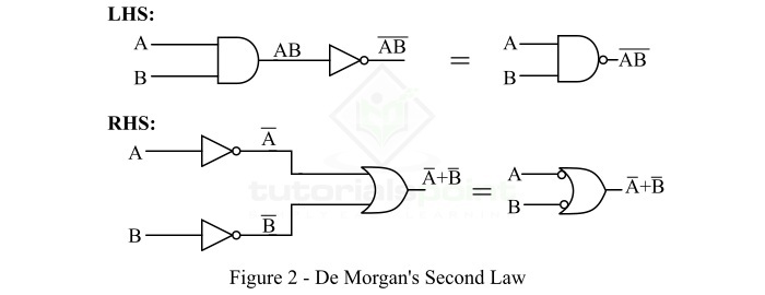
Hence, DeMorgan's second law proves that the NAND gate is equivalent to a bubbled OR gate. The following truth table shows the proof of this law.
| Left Side | Right Side | ||||
|---|---|---|---|---|---|
| Input | Output | Input | Output | ||
| A | B | AB | A' | B' | A' + B' |
| 0 | 0 | 0 | 1 | 1 | 1 |
| 0 | 1 | 1 | 1 | 0 | 1 |
| 1 | 0 | 1 | 0 | 1 | 1 |
| 1 | 1 | 1 | 0 | 0 | 0 |
This truth table proves that the Boolean expression on the left side is equivalent to that on the right side of the expression of DeMorgan's second law.
Similar to the first law, we may extend the DeMorgan's second law for any number of variables or combination of variables.
For example,
$$\mathrm{\overline{ABCDE \dotso} \: = \: \overline{A} \: + \: \overline{B} \: + \: \overline{C} \: + \: \overline{D} \: + \: \overline{E} \: + \: \dotso}$$
And, for a combination of variables,
$$\mathrm{\overline{\lgroup ABC \rgroup} \overline{\lgroup DE \rgroup} \overline{\lgroup FG \rgroup \dotso} \: = \: \overline{ABC} \: + \: \overline{DE} \: + \: \overline{FG}}$$
Hence, from the above discussion, we can conclude that DeMorgan's second law transforms a product form of variables or combination of variables under a NOT sign into a sum form.
Therefore, DeMorgan's laws transforms an AND operation into an OR operation, and an OR operation into an AND operation. This principle is called duality.
Example 1
Apply DeMorgan's theorem to the following Boolean expression,
$$\mathrm{F \: = \: \overline{AB \overline{ \lgroup C \: + \: D \rgroup}EF}}$$
Solution
Given expression is,
$$\mathrm{F \: = \: \overline{AB \overline{ \lgroup C \: + \: D \rgroup}EF}}$$
As the given expression has AND operation under a NOT sign, thus on applying DeMorgan's second law, we get,
$$\mathrm{F \: = \: \overline{AB} \: + \: \lgroup C \: + \: D \rgroup \: + \: \overline{EF}}$$
This is the equivalent or the dual of the given expression.
Example 2
Apply DeMorgan's theorem to the following Boolean expression,
$$\mathrm{F \: = \: \overline{AB \: + \: \overline{CD}}}$$
Solution
Given expression is,
$$\mathrm{F \: = \: \overline{AB \: + \: \overline{CD}}}$$
The given expression is in the form of a sum of variables under a NOT sign, thus on applying DeMorgan's first law, we get the dual of this expression.
$$\mathrm{F \: = \: \overline{AB} \cdot \overline{\overline{CD}} \: = \: \overline{AB} \cdot CD}$$
In this chapter, we explained the two laws of DeMorgan's Theorem and showed how they are helpful in performing different operations in digital logic circuits.
Logical Expression in SOP and POS Form
Before focusing on logical expression in SSOP (Standard Sum of Products) form and SPOS (Standard Product of Sum) form, let us have a brief introduction the "Sum of Products" and "Product of Sum" forms.
SOP (Sum of Products) Form
The SOP or Sum of Products form is a form of expressing a logical or Boolean expression. In SOP, different product terms of input variables are logically ORed together. Therefore, in the case of SOP form, we first logically AND the input variables, and then all these product terms are summed together with the help of logical OR operation.
For example −
$$\mathrm{\mathit{f} \lgroup A,B,C \rgroup \: = \: ABC \: + \: \bar{A}BC \: + \: AB \bar{C}}$$
This is a logical expression in three variables. Here, ABC, A'BC, and ABC' are the three product terms which are summed together to get the expression in SOP form.
POS (Product of Sum) Form
The POS or Product of Sum form is another form used to represent a logical expression. In POS form, different sum terms of input variables are logically ANDed together. Hence, if we want to express a logical expression in POS form, for that we first logically OR all the input variables and then these sum terms are ANDed using AND operation.
For example −
$$\mathrm{\mathit{f} \lgroup A,B,C \rgroup \: = \: \lgroup A \: + \: B \: + \: C \rgroup \lgroup \bar{A} \: + \: B \: + \: C \rgroup \lgroup A \: + \: B \: + \: \bar{C} \rgroup}$$
Here, f is a logical expression in three variables. From this example, it can be seen that there are three sum terms which are ANDed together to obtain the POS form of the given expression.
Now, let us discuss the Standard Sum of Products (SSOP) form and Standard Product of Sum (SPOS) form in detail.
A Boolean or logical expression can be represented into two standard forms namely,
- SSOP Form
- SPOS Form
Standard Sum of Products (SSOP) Form
The Standard Sum of Products (SSOP) form is a form of expressing a logical expression in which the logical expression is represented as the sum of a number of product terms where each product term will contain all the variables of the logical expression either in complemented or un-complemented form.
Since, each product term of the SSOP form contains all the variables, hence it is also known as Expanded Sum of Products form. The SSOP form is also known Disjunctive Canonical Form (DCF) or Canonical Sum of Products Form or Normal Sum of Products Form.
We can simply obtain the standard sum of products form of a logical expression from the truth table by determining the sum of all the terms that correspond to those combinations for which the given logical expression (say f) has the value 1.
We can also obtain the standard sum of products (SSOP) form of an expression from the sum of products (SOP) form by using Boolean algebra.
For example,
$$\mathrm{\mathit{f} \lgroup A,B,C \rgroup \: = \: A \bar{B} \: + \: B \bar{C}}$$
This is a logical expression in three variables, but it is expressed in SOP form. We can convert this expression into SSOP form using Boolean algebra as follows.
$$\mathrm{\mathit{f}\lgroup A,B,C \rgroup \: = \: A \bar{B} \lgroup C \: + \: \bar{C} \rgroup \: + \: B \bar{C} \lgroup A \: + \: \bar{A} \rgroup}$$
$$\mathrm{\mathit{f}\lgroup A,B,C \rgroup \: = \: A \bar{B}C \: + \: A \bar{B} \: \bar{C} \: + \: AB \bar{C} \: + \: \bar{A}BC}$$
This is the Standard Sum of Products form of the given logical expression. We can notice that in the SSOP form, each product term contains all the variables of the logic function either in complemented or un-complemented form. Each of these product terms is called a minterm. A logical function or expression in n' variables can have maximum 2n minterms. The sum of minterms of a logical expression whose value is 1 is called the standard sum of products form of the expression.
Standard Product of Sum (SPOS) Form
The Standard Product of Sums (SPOS) form is a form of expressing a logical function in which the logical expression is represented as the product of a number of sum terms where each sum term will contain all the variables of the logical expression either in complemented or un-complemented form.
SPOS form is also known as Conjunctive Canonical Form (CCF) or Expanded Product of Sums Form or Normal Product of Sums Form or Canonical Product of Sums Form.
The SPOS form of each term is derived by considering the combinations of variables for which the output is equal to 0. Each term is a sum of all the variables of the expression.
In the SPOS form, a variable appears in its complemented form if it has a value of 1 in the combination, and it appears in un-complemented form if it has a value of 0 in the combination.
In the case of standard product of sums form, a term which contains each of the n variables of the function in either complemented or un-complemented form is called a maxterm. For a logical function in n variables, there could be at the most 2nmaxterms. The product of maxterms of a logical expression whose value is 0 is called the standard product of sums form of the expression.
Similar to the SSOP form, we can obtain the standard product of sums form from the truth table of the logical expression by determining the product of all the sum terms that correspond to those combinations of variables for which the given logical expression (say f) has the value equal to 0.
Also, the SPOS form of a logical expression can be obtained by using Boolean algebra.
For example,
$$\mathrm{\mathit{f} \lgroup A,B,C \rgroup \: = \: \lgroup \bar{A} \: + \: B \rgroup \: + \: \lgroup A \: + \: \bar{C} \rgroup}$$
This is a logical expression in three variables, but it is expressed in POS form. We can convert this expression into SPOS form by using Boolean algebra as follows.
$$\mathrm{\mathit{f} \lgroup A,B,C\rgroup \: = \: \lgroup \bar{A} \: + \: B \: + \: C \bar{C} \rgroup \: + \: \lgroup A \: + \: \bar{C} \: + \: B \bar{B} \rgroup}$$
$$\mathrm{\mathit{f} \lgroup A,B,C \rgroup \: = \: \lgroup \bar{A} \: + \: B \: + \: C \rgroup \lgroup \bar{A} \: + \: B \: + \: \bar{C} \rgroup \lgroup A \: + \: B \: + \: \bar{C} \rgroup \lgroup A \: + \: \bar{B} \: + \: \bar{C} \rgroup}$$
This is the Standard Product of Sums (SPOS) form of the given logical expression. Here, we can note that in the SPOS form, each sum term contains all the variables of the logic function either in complemented or un-complemented form.
Digital Electronics - K-Map Minimization
What is Karnaugh Map?
In realization of digital electronic systems, the simplification of Boolean expressions is one of the most crucial steps because it reduces the hardware complexity and cost of production. There are several tools and methods available for simplifying complex Boolean expression. K-Map or Karnaugh Map is one of such simplification methods. K-Map was developed by Maurice Karnaugh in the year of 1953. It is a visual or graphical method used to simplify the Boolean expressions.
K-Map is one of the most efficient simplification tools when the number of variables in the Boolean expression are less than or equal to four. However, for five, six, and more variables, the K-Map becomes quite difficult.
The K-Map or Karnaugh map makes the use of two dimensional table for simplification of the Boolean functions. The size of this table increases considerably with the increase in the number of variables in the Boolean functions.
Some typical examples of K-Map of two variable, three variable, and four variables are shown in Figure-1.

From Figure-1, it is clear that the number of squares or cells in the Karnaugh map depends on the number of variables in the expression.
If n is the number of variables in the given Boolean function, then the corresponding Karnaugh map (K-Map) will have 2n squares or cells. For examples, if the number of variables in the Boolean function is 3, then the corresponding K-Map will have 8 (= 23) cells.
Structure of Karnaugh Map
All the Karnaugh maps or K-Maps have a generalized similar structure as shown in Figure-1. A typical K-Map has a table of certain cells. On the top-left corner of this table, a set of variables are represented as A, B, C, D. These variables are basically the input variables involved in the logical expression that requires to be simplified.
The values of these inputs variables in binary form are represented along their respective sides, i.e., on the top and left of the table.
From the above examples, it can be observed that the binary numbers along the top and left of the K-Map are not in their normal binary order, instead they are in the gray code. The Gray code is used to ensure that the two physically adjacent cells are actually adjacent. This makes the process of grouping easier during minimization of the Boolean expression.
For providing simplicity in reading the K-Map, each cell of the K-Map is assigned a decimal number represented at the bottom-right corner of the cell. For example, in the three variable K-map (figure-1), the second cell of the K-Map represents a bit pattern 001, hence this cell is represented by its decimal equivalent 1.
K-Map Simplification
The procedure of K-Map or Karnaugh map simplification is started with the entering the values of the variables, either in their SOP (Sum of Products) form or in POS (Product of Sums) form, in the right K-map cells. After that we need to group the maximum number of 1s (in the case of SOP form) or the maximum number of 0s (in the case of POS form). Each of these groups must be in powers of 2 and must be carried on in decreasing order only.
Once the grouping is done, each group has to be expressed in terms of combinations of input variables which are corresponding to the common binary values along the associated rows and columns. At last, all the combinations express the output expression of the Boolean function.
Advantages of Karnaugh Map
The following are the important advantages of the Karnaugh map −
- For simplifying Boolean expression, the K-map does not require the knowledge of theorems of Boolean algebra.
- Karnaugh map involves less number of steps in simplification process of logical expressions as compared to other simplification techniques.
Limitations of Karnaugh Map
The following are the major limitations of the Karnaugh map −
- The most significant limitation of the Karnaugh map is that it is only efficient when the Boolean expression has less number of variables. It becomes quite complicated with the higher number of variables in the logical expression.
- The simplification of a Boolean function having more than or equal to five variables using K-Map is quite complex.
- It is very difficult to get equations correct with more than 5 variables using the K-map.
Conclusion
The Karnaugh map or K-Map is an efficient tool for simplifying Boolean expression up to 4 variables. It is an easy method for simplification of logic expression because it does not make the use of Boolean algebra theorems. Another advantage of K-Map is that it is a visual method of simplification. However, the K-map becomes complex and inefficient when the variables in the logical expression are equal to or more than 5.
3 Variable K-Map in Digital Electronics
A K-Map or Karnaugh Map is a graphical method that used for simplifying the complex algebraic expressions in Boolean functions. This method avoid the use of complex theorems and equations manipulations. A K-Map is basically a special form of a truth table that can easily map out the values of parameters and gives a simplified Boolean expression.
K-Map method is best suited for such Boolean functions that have two to four variables. However, it can be used for Boolean functions having five or six variables as well, but its process becomes more difficult with the increased number of variables in the function.
Therefore, in practice, we mostly use Two-Variable K-Map, Three-Variable K-Map, and Four-Variable K-Map. But, sometimes, the Five-Variable K-Map and Six-Variable K-Map are also used to derive the Boolean expressions.
Here, we will discuss the 3 Variable K-Map and its application to simplify a complex Boolean function.
Three-Variable K-Map
We can use the K-Map to simplify a Boolean function of three-variables. A Boolean function in three variables (A, B, C) can be expressed in the standard sum of product (SOP) form that can have total eight possible combinations, which are as follows −
$$\mathrm{(A'B'C'), (A'B'C), (A'BC'), (A'BC), (AB'C'), (AB'C), (ABC'), (ABC)}$$
We can designate each of these combinations by m0, m1, m2, m3, m4, m5, m6, and m7 respectively. Each of these terms are called a min-term. In these combinations, A is called MSB (Most Significant Bit) and C is called LSB (Least Significant Bit).
In terms of POS (Product of Sum) form, the eight possible combinations of the three variables Boolean expression are as follows −
$$\mathrm{(A+B+C), (A+B+C'), (A+B'+C), (A+B'+C'), (A'+B+C), (A'+B+C'), (A'+B'+C), (A'+B'+C')}$$
Each one of these combinations are often designated by M0, M1, M2, M3, M4, M5, M6, and M7 respectively. Each of these terms is called a maxterm. Similar to the minterm, A is called MSB (Most Significant Bit) and C is called LSB (Least Significant Bit).
Therefore, a three variable K-Map has eight (23) squares or cells, and each square on the K-Map represents a minterm of a maxterm as shown in the following figure.

Here, the small number on the bottom right corner of each cell indicates the minterm or maxterm designation.
The binary numbers along the top of the K-Map indicates the condition of variables B and C for each column. The binary number along the left side of the map against each row represents the condition of the variable A for that row.
For example, the binary number of 10 on the top of the fourth column in the above figure indicates that the variable B appears in non-complimented form and the variable C appears in complimented form in all the minterms in that column. The binary number 0 on the left of the first row on the K-map indicates that the variable A appears in its complimented form in all the minterms, and the binary number 1 on the left of the second row on the K-Map indicates that the variable A appears in its non-complimented form in all the minterms.
Also, note that the binary numbers on top of the K-map are not in the normal binary order, but they are actually in the Gray code. The use of Gray code in K-map ensures that the two physically adjacent cells are actually adjacent which means their minterms or maxterms differs by one variable only.
Numerical Example
Map the following three-variable Boolean expression on K-Map.
$$\mathrm{f \: = \: \overline{A} \: \overline{B} \: C \: + \: A \: \overline{B} \: C \: + \: \overline{A} \: B \: \overline{C} \: + \: A \: \overline{B} \: \overline{C} \: + \: A \: B \: C}$$
Solution
In the given Boolean expression, the minterms are −
$$\mathrm{\overline{A} \: \overline{B} \: C \: = \: 001; \: A \: \overline{B} \: C \: = \: 101; \: \overline{A} \: B \: \overline{C} \: = \: 010; \: A \: \overline{B} \: \overline{C} \: = \: 100; \: ABC \: = \: 111}$$
Therefore,
$$\mathrm{m_{1} \: = \: \overline{A} \: \overline{B} \: C \: = \: 001}$$
$$\mathrm{m_{5} \: = \: A \: \overline{B} \: C \: = \: 101}$$
$$\mathrm{m_{2} \: = \: \overline{A} \: B \: \overline{C} \: = \: 010}$$
$$\mathrm{m_{4} \: = \: A \: \overline{B} \: \overline{C} \: = \: 100}$$
$$\mathrm{m_{7} \: = \: ABC \: = \: 111}$$
Hence, the expression is given by,
$$\mathrm{f \: = \: \sum \: m (1, \: 5, \: 2, \: 4, \: 7)}$$
The K-map of this expression is shown in the following figure −

Conclusion
From the above discussion, we may conclude that the three variable K-Map is a graphical method used to simplify the complex three variable Boolean function. A three-variable Kmap has eight squares or cells.
4 Variable K-Map in Digital Electronics
Several techniques have been developed to simplify a complex Boolean expression into its simplest form. K-Map or Karnaugh Map is one of such minimization or simplification techniques.
The K-Map or Karnaugh Map is a graph or chart which composed of an arrangement of adjacent cells. Where, each cell of the K-Map represents a particular combination of variables in either sum or product form. The K-map can be used to simplify Boolean functions involving any number of variables. But, the simplification of a Boolean function using K-map becomes tedious for problems involving five or more variables. Therefore, in actual practice, the K-map is limited to six variables.
The number of cells in a K-map depends upon the number of variables in the given Boolean function. A K-map will have 2n cells or squares, where n is the number of variables in the Boolean expression. Therefore, for a two variable function, the K-map will have 22 = 4 cells, for a three variable Boolean function, the K-map will have 23 = 8 cells, and for four variable Boolean function, the K-map will have 24 = 16 cells, and so on.
Here, we will discuss four variable K-Map and will use it to simplify Boolean functions in 4 variables.
Four Variable K-Map
A four variable K-map is used to simplify a complex Boolean expression in 4 variables. As we know, a four variable Boolean expression can have 24 = 16 possible combinations of variables.
For example, in SOP (Sum of Products) Form,
$$\mathrm{f(A,B,C,D) \: = \: \bar{A}\bar{B}\bar{C}\bar{D} \: + \: \bar{A}\bar{B}\bar{C}D \: + \: \bar{A}\bar{B}C\bar{D} \: + \: \dots \: + \: ABCD}$$
The minterm representation of this expression is as follows,
$$\mathrm{f(A,B,C,D) \: = \: m_{0} \: + \: m_{1} \: + \: m_{2} \: + \: \dotso \: + \: m_{15}}$$
In POS (Product of Sums) Form,
$$\mathrm{f(A,B,C,D) \: = \: (A \: + \: B \: + \: C \: + \: D)(A \: + \: B \: + \: C \: + \: \overline{D} )(A \: + \: B \: + \: \overline{C} \: + \: D) \: \dotso \: (\overline{A} \: + \: \overline{B} \: + \: \overline{C} \: + \: \overline{D})}$$
The maxterm representation of this expression is as,
$$\mathrm{f(A,B,C,D) \: = \: M_{0}\cdot M_{1}\cdot M_{2} \: \dotso \: M_{15}}$$
A 4 variable K-map has 16 cells, where each cell represents either a minterm or a maxterm of the function. The SOP (Sum of products) form and POS (Product of Sums) form of a four variable Boolean expression is shown in Figure 1.

Here, the binary number designations of the columns and rows are in the Gray code. This is known as adjacent ordering. In these K-maps, the binary numbers along the left side of the map indicate the conditions of variables A and B along any row, and the binary numbers along the top of the K-map indicate the conditions of the variables C and D along any column. The decimal numbers in the bottom right corners of the cells indicate the minterm or maxterm designation.
Now, let us consider an example to illustrate the utilization of the 4 variable K-map for simplification of a Boolean function.
Example 1
Simplify the following Boolean expression using the 4-variable K-map.
$$\mathrm{f \lgroup A,B,C,D \rgroup \: = \: \sum m \lgroup 2,3,6,7,8,10,13,15 \rgroup}$$
Solution
The SOP K-map representation of the given Boolean function is shown in Figure 2.

Explanation
The simplification of the function is done as per the following steps −
There are no isolated 1s in the K-Map.
The minterm m2 can form a 4-square with m3, m6, and m7. Make it and read it as −
$$\mathrm{\bar{A}C}()$$
The minterm m8 can form a 2-square with m10. Make it and read it as −
$$\mathrm{AB\bar{D}}()$$
The minterm m13 can form a 2-square with m15. Make it and read it as −
$$\mathrm{(A\bar{B}D)}$$
Write all the product in SOP form.
So the simplified SOP expression is,
$$\mathrm{f(A,B,C,D) \: = \: \bar{A}C \: + \: A\bar{B}D \: + \: AB\bar{D}}$$
Example 2
Minimize the following Boolean expression using the 4-variable K-map.
$$\mathrm{f(A,B,C,D) \: = \: \prod \: M(4,6,11,14,15)}$$
Solution
The POS K-map representation of the given Boolean function is shown in Figure 3.
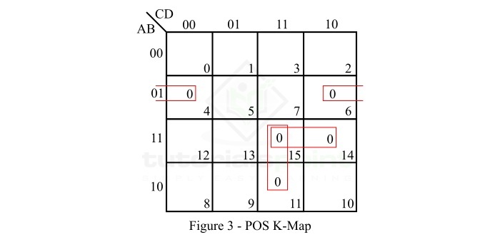
Explanation
In minimization of the given function is done as per the following step −
There are no isolated zeros in the K-map.
The maxterm M4 can form a 2-squate with M6. Make it and read it as −
$$\mathrm{(A \: + \: \bar{B} \: + \: D)}$$
The maxterm M11 can form a 2-square with M15. Make it and read it as −
$$\mathrm{(\bar{A} \: + \: \bar{C} \: + \: \bar{D})}$$
Now, only maxterm M14 is left. M14 can form 2-square with M6 or M15. If we make it with M15, then read it as −
$$\mathrm{(\bar{A} \: + \: \bar{B} \: + \: \bar{C})}$$
Finally, write all the sum terms in POS form.
So, the reduced POS expression of the given Boolean function is,
$$\mathrm{f(A,B,C,D) \: = \: (A \: + \: \bar{B} \: + \: D)(\bar{A} \: + \: \bar{C} \: + \: \bar{D})(\bar{A} \: + \: \bar{B} \: + \: \bar{C})}$$
Numerical Problems on K-Map
Q1. Reduce the following Boolean function using 4-variable K-map
$$\mathrm{f \lgroup A,B,C,D \rgroup \: = \: \sum m \lgroup 0,1,2,5,8,10,11,13,14,15 \rgroup }$$
Q2. Minimize the following Boolean expression using 4-variable K-Map.
$$\mathrm{f \lgroup A,B,C,D \rgroup \: = \: \prod \: M \lgroup 0,2,8,10,11,13,15 \rgroup}$$
Conclusion
This is all about the 4 variable K-map and its application to minimize a Boolean expression into its minimal form. From the above discussion, we can conclude that the 4-variable K-map is a graphical representation of a Boolean expression involving 4 variables and is represented in standard SOP or POS form. This is used to convert a standard SOP or POS form, or minterm form or maxterm form of a 4-variable Boolean expression into its minimal SOP or POS form.
5 Variable K-Map in Digital Electronics
K-Map or Karnaugh Map is a simplification technique used to minimize a given complex Boolean function. K-Map or Karnaugh Map is a graph or chart which is composed of an arrangement of adjacent cells, where each cell of the K-Map represents a particular combination of variables in either sum or product form. The K-map can be used to simplify Boolean functions involving any number of variables. But, the simplification of a Boolean function using K-map becomes very complex for expressions involving five or more variables. Therefore, in actual practice, the K-map is limited to six variables.
The number of cells in a K-map depends upon the number of variables in the given Boolean function. A K-map will have 2n cells or squares, where n is the number of variables in the Boolean expression. Therefore, for a two variable function, the K-map will have 22 = 4 cells, for a three variable Boolean function, the K-map will have 23 = 8 cells, and for four variable Boolean function, the K-map will have 24 = 16 cells, and so on.
Here, we will discuss five variable K-Map and will use it to simplify Boolean functions in 5 variables. So lets start with the introduction of 5 variable K-map.
Five Variable K-Map
A five variable K-map is used to minimize a 5-variable Boolean expression to its reduced form. The following are the important characteristics of a 5 variable K-map −
A five variable K-map have 32 (25) cells or squares, and each cell of the K-map represents either a minterm or a maxterm of the Boolean expression.
If the given Boolean function is expressed in SOP (Sum of Products) form, then the minterms of five variables Boolean function are designated as m0,m1,m2,m3 ... m31. Where, m0 is corresponding to $\mathrm{\lgroup \overline{A} \: \overline{B} \: \overline{C} \: \overline{D} \: \overline{E} \rgroup}$, m1 is corresponding to $\mathrm{\lgroup \overline{A} \: \overline{B} \: \overline{C} \: \overline{D} E \rgroup}$, and m31 is corresponding to $\mathrm{\lgroup ABCDE \rgroup}$.
On the other hand, if the 5 variable Boolean function is expressed in POS (Product of Sums) form, then the maxterms of the function are designated as M0, M1, M2, M31.
Where, M0 represents
$$\mathrm{\lgroup A \: + \: B \: + \: C \: + \: D \: + \: E \rgroup}$$
M1 represents
$$\mathrm{\lgroup A \: + \: B \: + \: C \: + \: D \: + \: \overline{E} \rgroup}$$
M31 represents
$$\mathrm{\lgroup \overline{A} \: + \: \overline{B} \: + \: \overline{C} \: + \: \overline{D} \: + \: \overline{E} \rgroup}$$.
The 32 cells of the five variable K-map are divided into two blocks of 16 cells each, which are arranged side by side. The left block represents minterms (or maxterms) from m0 to m15 (or M0 to M15. Wheck, thck, th). In the left block, the first variable (let A) is a 0. The right block represents minterms (or maxterms) from m16 to m31 (or M16 to M31), in this block A is a 1.
In the five variable K-map, we can form 2-squares, 4-squares, 8-squares, 16-squares, or 32-squares by involving its two blocks. Also, squares are considered adjacent in these two blocks, when one block superimposes on the top of another.
A five variable SOP K-map is shown in Figure 1.
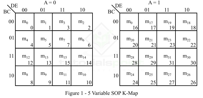
A five variable POS K-map is represented in Figure 2.
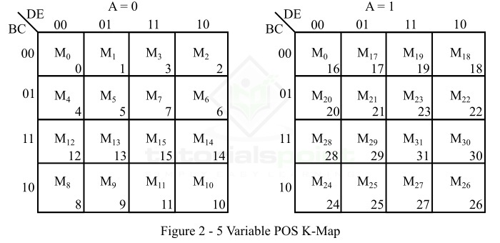
Now, let us discuss some solved examples to understand the application of a 5 variable K map in reducing a given 5-variable Boolean function in either SOP form or POS form.
Example 1
Reduce the following 5 variable Boolean function in SOP form using the five variable K map.
$$\mathrm{f \lgroup A,B,C,D,E \rgroup \: = \: \sum \: m \lgroup 0,1,2,4,7,8,12,14,15,16,17,18,20,24,28,30,31 \rgroup }$$
Solution
The SOP K-map representation of the given SOP Boolean function is shown in Figure 3.
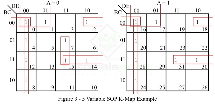
Explanation
The minimization of the given 5 variable Boolean function using the five variable K-map (Figure 3) is done as per the following steps −
There are no isolated 1s in the K-map.
The minterm m0 can form an 8-square with m4, m8, m12, m16, m20, m24, and m28. So make it and read it as −
$$\mathrm{\lgroup \overline{D} \: \overline{E} \rgroup} $$
The minterms m0, m1, m16, and m17 form a 4-square. Make it and read it as −
$$\mathrm{\lgroup \overline{B} \: \overline{C} \: \overline{D} \rgroup} $$
The minterms m0, m2, m16, and m18 form a 4-square. Make it and read it as −
$$\mathrm{\lgroup \overline{B} \: \overline{C} \: \overline{E} \rgroup}$$
The minterms m7 and m15 form a 2-square. Make it and read it as −
$$\mathrm{\lgroup \overline{A}CDE \rgroup} $$
The minterms m14, m15, m30 and m31 form a 4-square. Make it and read it as −
$$\mathrm{\lgroup BCD \rgroup} $$
Finally, write all the product terms in SOP form.
Hence, the minimal SOP expression of the given 5 variable Boolean function is,
$$\mathrm{f(A,B,C,D,E) \ = \: \overline{A}CDE \: + \: \overline{B} \: \overline{C} \: \overline{D} \: + \: \overline{B} \: \overline{C} \: \overline{E} \: + \: BCD \: + \: \overline{D} \: \overline{E}}$$
Example 2
Minimize the following 5 variable Boolean function in POS form using the five variable K map.
$$\mathrm{f \lgroup A,B,C,D,E \rgroup \: = \: \prod \: M \lgroup 3,5,6,9,10,11,13,19,21,22,23,25,26,27,29 \rgroup}$$
Solution
The POS K-map representation of the given POS Boolean function is shown in Figure 4.
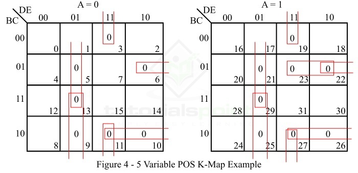
Explanation
The minimization of the given 5 variable Boolean function using the five variable K-map (figure-4) is done as per the following steps −
There are no isolated zeros in the K-map.
The maxterms M9, M13, M25, and M29 form a 4 square. Make it and read it as −
$$\mathrm{\lgroup \overline{B} \: + \: D \: + \: \overline{E} \rgroup} $$
The maxterms M3, M11, M19, and M27 form a 4 square. Make it and read it as −
$$\mathrm{\lgroup C \: + \: \overline{D} \: + \: \overline{E} \rgroup} $$
The maxterms M5, M13, M21, and M29 form a 4 square. Make it and read it as −
$$\mathrm{\lgroup \overline{C} \: + \: D \: + \: \overline{E} \rgroup}$$
The maxterms M6 and M22 form a 2 square. Make it and read it as −
$$\mathrm{\lgroup B \: + \: \overline{C} \: + \: \overline{D} \: + \: E \rgroup}$$
The maxterms M10, M11, M26, and M27 form 4 square. Make it and read it as −
$$\mathrm{\lgroup \overline{B} \: + \: C \: + \: \overline{D} \rgroup}$$
The maxterms M22 and M23 form 2 square. Make it and read it as −
$$\mathrm{\lgroup \overline{A} \: + \: B \: + \: \overline{C} \ + \: \overline{D} \rgroup}$$
Finally, write all the sum terms in POS form.
Therefore, the minimal POS expression of the given Boolean function in five variables is,
$$\mathrm{f \lgroup A,B,C,D,E \rgroup \: = \: \lgroup \overline{B} \: + \: D \: + \: \overline{E} \rgroup \lgroup C \: + \: \overline{D} \: + \: \overline{E} \rgroup \lgroup \overline{C} \: + \: D \: + \: \overline{E} \rgroup \lgroup B \: + \: \overline{C} \: + \: \overline{D} \: + \: E \rgroup \lgroup \overline{B} \: + \: C \: + \: \overline{D} \rgroup \lgroup \overline{A} \: + \: B \: + \: \overline{C} \: + \: \overline{D} \rgroup}$$
Numerical Problems on K-Map
Try to solve the following numerical problems to get better command on the utilization of five variable K-map to reduce a Boolean expression.
Q1. Reduce the following five variable Boolean expression in SOP form using K-Map.
$$\mathrm{f \lgroup A,B,C,D,E \rgroup \: = \: \sum m \lgroup 0,3,4,6,8,10,11,12,15,17,18,22,25,26,27,30,31 \rgroup }$$
Q2. Reduce the following five variable Boolean expression in POS form using K-map.
$$\mathrm{f \lgroup A,B,C,D,E \rgroup \: = \: \prod \: M\lgroup 0,1,2,4,6,7,9,10,11,13,15,16,18,19,25,26,28,29,31 \rgroup }$$
Conclusion
This is all about the five variable K-map. From the above discussion, we can conclude that a five variable Boolean function can be reduced to the minimal form using the 5 variable K-map. A five variable K-map has 32 squares or cells from 0 to 31. These 32 cells are arranged in two blocks 16 cells each. However, the split form of the 5 variable K-map into two blocks makes the use of it to minimize a Boolean function slightly complex.
6 Variable K-Map in Digital Electronics
Read this chapter to learn how you can use the K-Map (Karnaugh Map) to reduce a Boolean function in six variables. Let's start with a brief introduction to Karnaugh Map (K-Map).
Karnaugh Map (K-Map)
The Karnaugh Map or K-Map is a graphical method of reducing a Boolean function to its minimal form. The K-Map can be defined as a chart or a graph that is composed of an arrangement of adjacent squares or cells, where each cell represents a particular combination of variables of the Boolean expression either in sum or product form. A typical 2 Variable K-Map is represented in Figure-1.

In actual practice, we generally use a K-map upto 6 variables. However, K-map can be used for any number of variables, but for variables 5 or more, it becomes tedious.
Now, let us discuss the six variable K-map and its application to reduce a Boolean function to the minimal form.
Six Variable K-Map
A six variable K-Map is used to reduce a Boolean expression of six variables (say A, B, C, D, E, F). It has 64 (26) adjacent cells or squares. Where, each cell represents a combination of variables of the function.
For a 6-variable Boolean function in SOP form, the possible combinations of the input variables are as follows −
$$\mathrm{\bar{A}\bar{B}\bar{C}\bar{D}\bar{E}\bar{F}, \: \bar{A}\bar{B}\bar{C}\bar{D}\bar{E}F, \: \bar{A}\bar{B}\bar{C}\bar{D}E\bar{F}, \: \dots \: ABCDEF}$$
The minterm designations of these combinations of variables are m0, m1, m2 m63 respectively.
Similarly, for a 6-variables Boolean function in POS form, the possible combinations of input variables are as follows −
$$\mathrm{\left ( A \: + \: B \: + \: C \: + \: D \: + \: E \: + \: F \right ), \: \left ( A \: + \: B \: + \: C \: + \: D \: + \: E \: + \: \bar{F} \right ), \: \left ( A \: + \: B \: + \: C \: + \: D \: + \: \bar{E} \: + \: F \right ), \: \dots \: \left ( \bar{A} \: + \: \bar{B} \: + \: \bar{C} \: + \: \bar{D} \: + \: \bar{E} \: + \: \bar{F} \right )}$$
The maxterm designations of these combinations of variables are M0, M1, M2, ... M63 respectively.
As already mentioned, the six variable K-map has 64 cells which are divided into 4-blocks of 16 squares each. Each cell on the K-map represents a minterm or a maxterm. In the case of 6 variable K-map, the values of variables A and B remain the same for all minterms (or maxterms) in each block of 16 squares.
The 64 cells of a six variable K-map are divided into 4 blocks as follows −
Block 1 − This is the top left block. This block represents minterms from m0 to m15, (or maxterms from M0 to M15). In this block, the variable A is a 0 and the variable B is also a 0.
Block 2 − This is the top right block. This block represents minterms from m16 to m31, (or maxterms from M16 to M31). In this block, the variable A is a 0 and the variable B is a 1.
Block 3 − This is the bottom left block. This block represents minterms from m32 to m47, (or maxterms from M32 to M47). In this block, the variable A is a 1 and the variable B is a 0.
Block 4 − This is the bottom right block. This block represents minterms from m48 to m63, (or maxterms from M48 to M63). In this block, the variable A is a 1 and the variable B is also a 1.
While simplification, the 6-variable K-map may contain 2-squares, 4-squares, 8-squares, 16- squares, 32-squares, or a 64-square by involving all the four blocks of the map.
In a six variable K-Map, when a block is superimposed on the top of another block, which is either above or below or beside of the first block, and the squares coincide with one another. Then, the squares are considered adjacent in the two blocks. It is also important to note that the diagonal elements such as m10 and m58, m15 and m63, m18 and m34, m29 and m45 are not adjacent to each other.
A six variable SOP K-map is represented in Figure-2.

A six variable POS K-map is represented in Figure-3.

Now, let us understand the utilization of the six variable K-map for minimization of a six variable Boolean function with the help of solved numerical examples.
Example 1
Minimize the following 6 variable Boolean function using K-map.
$$\mathrm{f \: = \: \sum \: m(1, 3, 4, 5, 6, 9, 11, 12, 14, 15, 17, 19, 20, 21, 22, 23,25, 27, 28, 30, 33, 35, 36, 38, 41, 43, 44, 46, 49, 51, 52, 54, 57, 59, 60, 62)}$$
Solution
The 6-variable SOP K-map representation of the given Boolean function is shown in Figure-4.

The reduction of this function is done as per the following steps −
There are no isolated 1s in the K-map.
The minterm m1 forms a 16-square with minterms m3, m9, m11, m17, m19, m25, m27, m33, m35, m41, m43, m49, m51, m57, and m59. Make it and read it as −
$$\mathrm{\bar{D}F}$$
The minterm m4 forms a 16-square with minterms m6, m12, m14, m20, m22, m28, m30, m36, m38, m44, m46, m52, m54, m60, and m62. Make it and read it as −
$$\mathrm{\bar{F}D}$$
The minterm m5 can form a 4-square with minterms m4, m20, and m21, or with m1, m17, and m21. We will make it with minterms m4, m20, and m21, and read it as −
$$\mathrm{\bar{A}\bar{C}D\bar{E}}$$
The minterm m21 forms a 4-square with minterms m17, m19, and m23. Make it and read it as −
$$\mathrm{\bar{A}B\bar{C}F}$$
The minterm m15 can make a 2-square with the minterm m11 or m14. We will make it with m14, and read it as −
$$\mathrm{\bar{A}\bar{B}CDE}$$
Write all the product terms in SOP form.
Therefore, the minimal SOP expression is,
$$\mathrm{f \left ( A,B,C,D,E,F \right ) \: = \: \bar{D}F \: + \: D\bar{F} \: + \: \bar{A}\bar{C}D\bar{E} \: + \: \bar{A}B\bar{C}F \: + \: \bar{A}\bar{B}CDE}$$
Example 2
Minimize the following six variable Boolean function using K-map.
$$\mathrm{f \: = \: \Pi \: M(0, 2, 7, 8, 10, 13, 16, 18, 24, 26, 29, 31,32, 34, 37, 39, 40, 42, 45, 47, 48, 50, 53, 55, 56, 58, 61, 63)}$$
Solution
The 6-variable POS K-map representation of the given Boolean function is shown in Figure-5.
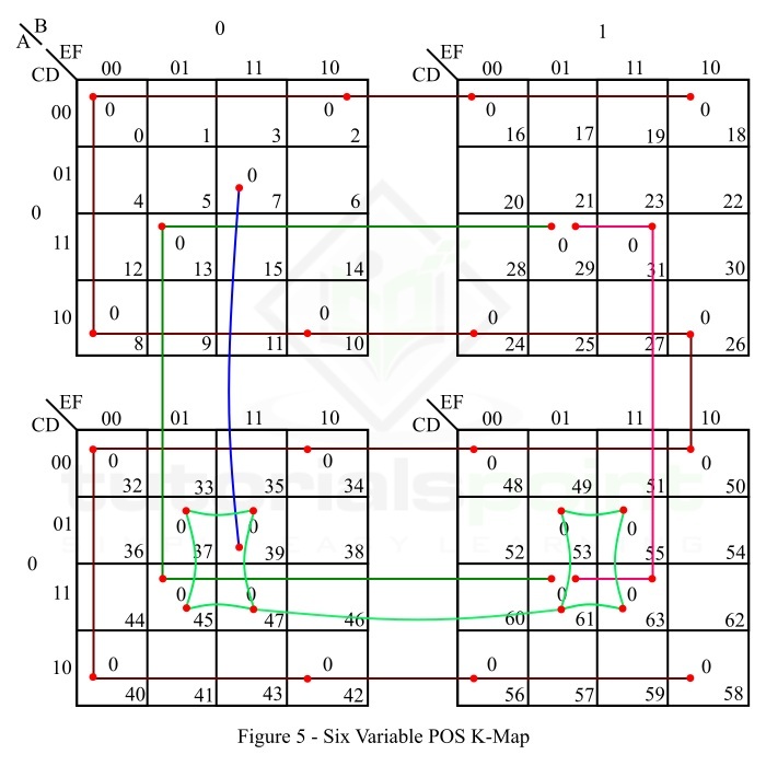
The reduction of this function is done as per the following steps −
There are no isolated 0s in the K-map.
The maxterm M0 forms a 16-square with maxterms M2, M8, M10, M16, M18, M24, M26, M32, M34, M40, M42, M48, M50, M56, M58. Make it and read it as −
$$\mathrm{\left ( D \: + \: F \right )}$$
The maxterm M37 forms an 8-square with maxterms M39, M45, M47, M53, M55, M61, and M63. Make it and read it as −
$$\mathrm{\left (\bar{A} \: + \: \bar{D} \: + \: \bar{F} \right )}$$
The maxterm M13 makes a 4-square with maxterms M29, M45, and M61. Make it and read it as −
$$\mathrm{\left(\bar{C} \: + \: \bar{D} \: + \: E \: + \: \bar{F} \right )}$$
The maxterm M31 makes a 4-square with M29, M61, and M63. Make it and read it as −
$$\mathrm{\left( \bar{B} \: + \: \bar{C} \: + \: \bar{D} \: + \: \bar{F} \right )}$$
The maxterm M7 forms a 2-square with the maxterm M39. Make it and read it as −
$$\mathrm{\left( B \: + \: C \: + \: E \: + \: \bar{D} \: + \: \bar{E} \: + \: \bar{F} \right )}$$
Write all the sum terms in POS form.
Thus, the minimal POS expression for the given Boolean function is,
$$\mathrm{f \left ( A,B,C,D,E,F \right ) \: = \: \left ( D \: + \: F \right )\left ( \bar{A} \: + \: \bar{D} \: + \: \bar{F} \right )\left( \bar{C} \: + \: \bar{D} \: + \: E \: + \: \bar{F} \right )\left( \bar{B} \: + \: \bar{C} \: + \: \bar{D} \: + \: \bar{F} \right )\left( B \: + \: C \: + \: E \: + \: \bar{D} \: + \: \bar{E} \: + \: \bar{F} \right )}$$
This is all about six variable K-map and its application in minimization of Boolean functions. Try solving the following tutorial problems to excel in the concept of six variable K-map and its application to reduce Boolean expressions.
Numerical Problems on K-Map
Q. 1 − Minimize the following six variable Boolean function in SOP form using K-map.
$$\mathrm{f \left ( A,B,C,D,E,F \right ) \: = \: \sum m(1, 3, 5, 7, 9, 10, 11, 12, 14, 16, 17, 19, 20, 22, 24, 25, 26, 31, 32,34, 36, 37, 39, 40, 42, 45, 49, 50, 53, 54, 57, 60, 61, 63)} $$
Q. 2 − Minimize the following six variable Boolean function in POS form using K-map.
$$\mathrm{f \left ( A,B,C,D,E,F \right ) \: = \: \Pi M(0, 1, 3, 4, 5, 6, 8, 9, 10, 12, 14, 15, 17, 20, 21, 22, 25, 26, 27,29, 30, 32, 33, 35, 36, 37, 39, 40, 41, 42, 45, 47, 48, 50, 52, 53, 55, 56, 58, 59, 60, 62 )}$$
Don't Care Condition in K-Maps
K-Map or Karnaugh Map is a graphical method of simplifying Boolean expression. A K-Map composed of an arrangement of adjacent squares or cells, where each cell represent a particular combination of variables in sum or product form.
In the K-map method, there is a useful condition namely, Dont Care Condition, which helps in simplifying a Boolean function. The dont care condition makes the grouping of variables in K-map easy. In this tutorial, we will understand the "dont care" concept in K-map reduction with the help of solved examples.
Sometimes, in a Boolean expression for certain input combinations, the value of the output is not specified either due to invalid input combinations or due to the precise value of output is of no importance. These input combinations for which the values of the Boolean function are not specified are called dont care combinations. Dont care combinations are also referred to as optional combinations. In K-map, dont care combinations are represented by "X" or "d" or "".
For example, in 8421 binary code, the binary combination 1010, 1011, 1100, 1101, 1110, and 1111 are the invalid terms and their corresponding outputs are dont care combinations. Similarly, in Excess-3 code, the combinations 0000, 0001, 0010, 1101, 1110, and 1111 do not occur, hence these are called dont care combinations.
When we deal with SOP (Sum of Products) K-map, each dont care term is treated as a 1, if it helps in reduction of the expression, otherwise it is considered as a 0 and left alone.
On the other hand, when we are using POS (Product of Sums) K-map, each dont care term is considered as a 0, if it is helpful in reduction of the expression, otherwise it is treated as a 1 and left alone.
Also, we can convert a Standard Sum of Products (SSOP) expression with dont care terms into a Standard Product of Sums (SPOS) expression by keeping the dont care terms as they are, and writing the missing minterms of the SSOP form as the maxterms of the SPOS form.
Similarly, we can convert a standard product of sums (SPOS) expression with dont care terms into a standard sum of products (SSOP) expression by keeping the dont care terms of the SPOS expression as they are, and writing the missing maxterms of the SPOS expression as the minterms of the SSOP expression.
Now, let us discuss some solved examples to understand the dont care condition in K-map.
Example 1
Minimize the following 4-variable Boolean expression in SOP form using K-map.
$$\mathrm{\mathit{f}\lgroup A,B,C,D\rgroup=\sum m \lgroup 0,1,4,5,6,10,13\rgroup +d \lgroup 2,3 \rgroup}$$
Solution
The SOP K-map representation of the given Boolean function is shown in Figure 1.
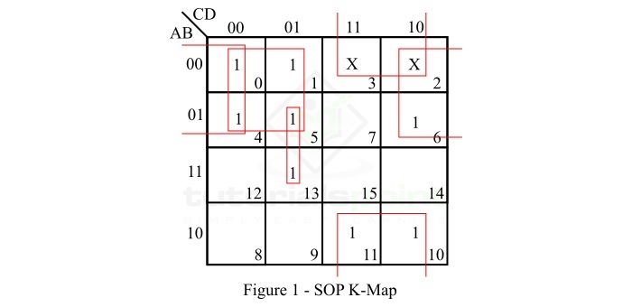
As we can see in the given expression, there are two dont care terms which are denoted by X on the K-map.
Explanation
The reduction of the expression is done as per the following steps −
- The minterms m0, m1, m4 and m5 form a 4-square. Make it and read it as $\mathrm{\lgroup \bar{A} \: \bar{C}\rgroup}$.
- The minterms m10 and m11 form a 4-sqaure with two dont care terms m2 and m3. Make it and read it as $\mathrm{\bar{B}C}$.
- The minterms m0, m4, m6 and the dont care term m2 together form a 4-square. Make it and read it as $\mathrm{\bar{A} \: \bar{D}}$.
- The minterms m5 and m13 form a 2-square. Make it and read it as $\mathrm{B\bar{C}D}$.
- Finally, write all the product terms in SOP form.
Therefore, the minimal Boolean expression is,
$$\mathrm{\mathit{f} \lgroup A,B,C,D \rgroup \: = \: \bar{A} \: \bar{C} \: + \: \bar{B}C \: + \: \bar{A} \: \bar{D} \: + \: B \bar{C}D}$$
Example 2
Minimize the following 4-variable Boolean expression in POS form using K map.
$$\mathrm{\mathit{f} \lgroup A,B,C,D \rgroup \: = \: \prod M \lgroup 1,5,6,12,13,14 \rgroup \: + \: d \lgroup 2,4 \rgroup}$$
Solution
The POS K-map representation of the given Boolean function is shown in Figure-2.
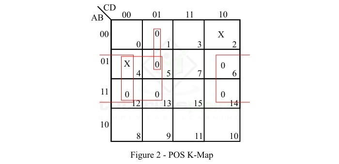
There are two dont care terms in the expression which are represented by X on the K-map.
Explanation
The reduction of the given function is done as per the following steps −
- The maxterms M5, M12 and M13 and dont care term M4 form a 4-square. Make it and read it as $\mathrm{\bar{B} \: + \: C}$.
- The maxterms M6, M12, and M14 and dont care term M4 form a 4-square. Make it and read it as $\mathrm{\bar{B} \: + \: D}$.
- The maxterms M1 and M5 form a 2-square. Make it and read it as $\mathrm{A \: + \: C \: + \: \bar{D}}$
- Write all the sum terms in POS form.
Therefore, the minimal Boolean expression is,
$$\mathrm{\mathit{f} \lgroup A,B,C,D \rgroup \: = \: \lgroup \bar{B} \: + \: C \rgroup \: + \: \lgroup \bar{B} \: + \: D \rgroup \: + \: \lgroup A \: + \: C \: + \: \bar{D} \rgroup}$$
Conclusion
This is all about dont care conditions in K-maps. As we discussed in the above sections of this tutorial, that the dont care condition is a significant and powerful concept that helps in minimization of Boolean function using K-map.
Quine-McCluskey Tabular Method
In this chapter, we will discuss the minimization of Boolean expressions using a tabular method also known as Quine-McCluskey method.
The Quine-McCluskey method is more beneficial in minimization of Boolean functions of more than six variables. This minimization technique overcomes the issues associated with K-Map for more than six variables.
Another major advantage of Quine-McCluskey method is that it is equally suitable both hand computation and machine computation, as it is programmable.
Theory of Quine-McCluskey Method
The Quine-McCluskey method is a systematic technique of minimizing complex Boolean expressions. It becomes a suitable method to perform minimization of Boolean expressions of large number of variables. It is also known as tabular method.
This minimization technique is based on the repeated use of the combining theorem (i.e., $\mathrm{XA \: + \: X\bar{A} \: = \: X}$, where X is a set of literals) on all adjacent pairs of terms. This process gives a set of all prime implicants, from which we can select a minimal sum.
Quine-McCluskey Method Procedure
The step-by-step procedure for minimizing a Boolean function by using the Quine McCluskey method is explained below −
Step 1 − List all the minterms of the given Boolean expression.
Step 2 − Group the minterms. In this step, we arrange all the minterms in groups according to the number of 1s in their binary form. For example, arrange all the minterms with no 1s together, all the minterms with only one 1s together, and so on. The number of 1s in a minterm is called the index of the minterm. Write these grouped minterms in the column 1 of the table.
Step 3 − Combine minterms. In this step, compare each minterm of the lowest index group with every minterm in the succeeding group. Whenever possible, combine two minterms in adjacent groups that differ by only 1-bit and replace the differing bit by a dash (-). This represents a dont care condition. Also, place a check mark () in front of the every minterm that has been combined with at least one minterm. Repeat this process until all possible minterm combinations are made. Write all the combined minterms in the column 2 of the table.
Step 4 − Compare and combine the minterms generated in the above step in the same manner. In this step, we combine two minterms which differ by only 1-bit and whose dashes are in the same position. We cannot combine two minterms having dashes in different positions.
Write the newly generated terms in the column 3 and put a check mark () next to each term that has been combined in the column 2. Continue this process with terms in column 3, 4, and so on until no further combination is possible. At the end, the terms that are not combined are called the prime implicants.
Step 5 − List all the prime implicants and create a prime implicant chart. If there is any dont care, it should not appear in the prime implicant chart.
Step 6 − Select the essential prime implicants which are the prime implicants that cover a minterm which is not covered by any other prime implicant.
Step 7 − Combine the essential prime implicants to obtain the final minimized expression.
Important Terms Related Quine-McCluskey Method
In the Quine-McCluskey method of Boolean expression minimization, several terms are used to convey information. Some key terms related to the Quine-McCluskey method are defined below −
Minterm − A minterm is a combination of Boolean variables that has 1 for true value and 0 for false value.
Maxterm − A maxterm is a combination of Boolean variables in which true values are designated by 0s and false values are designated by 1s.
Index − The number of 1s in a minterm is called its index.
Prime Implicant − A minterm that cannot be combined with any other minterm is called a prime implicant.
Essential Prime Implicant − A prime implicant that covers at least one minterm which is not covered by any other prime implicant is called an essential prime implicant.
Prime Implicant Chart − The graphical representation showing the relationship between the prime implicants and the minterms of the Boolean expression is called the prime implicant chart.
Dont Care Condition − A dont care condition is a bit or variable that can be ignored during minimization of the function. In Quine-McCluskey method, it is represented by a dash (-).
These are some important terms essential to work with the Quine-McCluskey method.
Let us now understand the application of Quine-McCluskey method to minimize a Boolean function through an example.
Example Based on Quine-McCluskey Method
Using the Quine-McCluskey technique minimize the following Boolean function.
$$\mathrm{f(A, B,C,D) \: = \: \sum \: m(0,1,5,7,10,14)}$$
Solution
The minimization of given Boolean function using the Quine-McCluskey method is explained below.
Step 1 − Grouping the given minterms in terms of number of 1s in ascending order and writing their binary form in column 1.
| Column 1 | |||||
|---|---|---|---|---|---|
| Index | Min Term | Binary Form | |||
| A | B | C | D | ||
| I0 | 0 | 0 | 0 | 0 | 0 |
| I1 | 1 | 0 | 0 | 0 | 1 |
| I2 | 5 | 0 | 1 | 0 | 1 |
| 10 | 1 | 0 | 1 | 0 | |
| I3 | 7 | 0 | 1 | 1 | 1 |
| 14 | 1 | 1 | 1 | 0 | |
Step 2 − Comparing and combining minterms of the column 1.
| Column 1 | Column 2 | |||||||||||
|---|---|---|---|---|---|---|---|---|---|---|---|---|
| Index | Min Term | Binary Form | Pairs | A | B | C | D | |||||
| A | B | C | D | |||||||||
| I0 | 0 | 0 | 0 | 0 | 0 | ✓ | 0, 1 (1) | 0 | 0 | 0 | - | P |
| I1 | 1 | 0 | 0 | 0 | 1 | ✓ | ||||||
| I2 | 5 | 0 | 1 | 0 | 1 | ✓ | 1, 5 (4) | 0 | − | 0 | 1 | Q |
| 10 | 1 | 0 | 1 | 0 | ✓ | 5, 7 (2) | 0 | 1 | − | 1 | R | |
| I3 | 7 | 0 | 1 | 1 | 1 | ✓ | ||||||
| 14 | 1 | 1 | 1 | 0 | ✓ | 10, 14 (4) | 1 | − | 1 | 0 | S | |
We can see there is no term that can be combined with any other term in the column 2 between two adjacent groups. Thus, all of them are prime implicants.
Step 3 − Creating the prime implicant chart.
| PI | Minterms | 0 | 1 | 5 | 7 | 10 | 14 |
| P | 0, 1 (1) | x | x | ||||
| Q | 1, 5 (4) | x | x | ||||
| R | 5, 7 (2) | x | x | ||||
| S | 10, 14 (4) | x | x |
We can see from the prime implicant chart that the minterms m10 and m14 are covered by S only. Hence, S is an essential prime implicant. It can also be observed that the remaining minterms of the function are covered by the minimal set of prime implicants P and R.
Therefore, the minimal expression will be,
$$\mathrm{f_{min} \: = \: P \: + \: R \: + \: S \: = \: (000 \: − \: ) \: + \: (01 \: − \: 1) \: + \:(1 \: − \: 10)}$$
$$\mathrm{\Rightarrow f_{min} \: = \: \overline{ABC} \: + \: \overline{A}BD \: + \: AC\overline{D}}$$
This is minimal Boolean expression for the given Boolean function and it can be realized using AND, OR, and NOT gates.
Advantages of Quine-McCluskey Method
The Quine-McCluskey method offers several advantages over other minimization techniques such as Karnaugh Map. Some of the key advantages of the Quine-McCluskey method are listed below −
- The Quine-McCluskey method provides a systematic minimization process to find a minimal version of a complex Boolean expression.
- It can be applied to Boolean functions of large number of variables where, the K-map technique becomes impractical.
- It is suitable for both hand computation and computerized computation.
- The Quine-McCluskey method is based on a systematic algorithm that helps to reduce human errors.
- It can also be applied to Boolean functions with dont care conditions, i.e., incomplete Boolean functions.
Disadvantages of Quine-McCluskey Method
However, the Quine-McCluskey method is a powerful simplification technique to minimize Boolean functions having several advantages over other minimization techniques.
But, it also has certain disadvantages, some of which are listed below −
- The primary disadvantage of the Quine-McCluskey method is computational complexity. It is because, we have to check all the possible combinations of minterms.
- Although the Quine-McCluskey method is better than K-Map for large number of variables. But it also becomes impractical for vary large number of variables, typically more than 7 variables.
- The Quine-McCluskey method involves extensive manual computation that makes it tedious and prone to human error.
- The Quine-McCluskey method is not much effective for certain types of Boolean functions.
- As the Quine McCluskey method involves an algorithmic approach for minimization rather than graphical approach. This makes it less intuitive.
Applications of Quine-McCluskey Method
The Quine-McCluskey method is one of the most effective minimization techniques in Boolean algebra. It provides a systematic approach to minimized complex Boolean functions of large number of variables. Some major applications of the Quine-McCluskey method are given below −
- Quine-McCluskey method is used to design and optimize digital circuits and systems. It helps reducing the number of logic gates used in the digital circuits.
- It is also used in computer programming to optimize conditional logics for better efficiency and faster speed.
- In digital signal processing, the Quine-McCluskey method is used to simplify Boolean expressions to develop efficient processing algorithms.
- Quine-McCluskey method is used to design efficient state machine.
Conclusion
In conclusion, the Quine-McCluskey method is a systematic and algorithmic approach for simplifying complex Boolean expressions. It is an effective minimization technique for Boolean functions of large number of variables.
The greatest advantage of the Quine-McCluskey method is that it supports both hand computation and machine computation, i.e., it is programmable. However, this method involves relatively complex computation which makes it tedious.
Minterms and Maxterms in Boolean Algebra
Any Boolean function or logical expression can be expressed in either canonical/standard sum of products form or canonical/standard product of sums form. The standard sum of products form of a logical expression contains different product terms which are added together, and each product term is referred to as a minterm. On the other hand, the standard product of sums form of a logical expression contains different sum terms which are multiplied together, and each sum term is called a maxterm. In this article, we will discuss about the minterm and max terms.
What is Minterm?
When a Boolean function or logical expression is expressed in the SSOP (Standard Sum of Product) Form or canonical form, then each term of the expression is called a minterm.
In other words, a product term of a logical expression in n variables, which contains each of the n variables in its either complemented or un-complemented form is called a minterm.
A minterm is often represented as mi, where, i is an integer in between 0 and 2(n-1). Here, "n" is the number of variables in the expression. Therefore, minterms can be denoted as m0, m1, m2,m3,... Here, the suffixes the decimal codes of the combinations of variables.
In a minterm, a variable will appear in its complemented form if its value is equal to 0. And, the variable will appear in its un-complimented form if its value is equal to 1.
Now, let us consider some example to understand how a logical expression is expressed in minterms.
For a logical expression in 2-variables (A and B), the possible minterms are,
$$\mathrm{m_{0} \: = \: \overline{A} \: \overline{B}}$$
$$\mathrm{m_{1} \: = \: \overline{A}B}$$
$$\mathrm{m_{2} \: = \: A\overline{B}}$$
$$\mathrm{m_{3} \: = \: AB}$$
For a logical expression in 3-variables (A, B, and C), the possible minterms are,
$$\mathrm{m_{0} \: = \: \overline{A} \: \overline{B} \: \overline{C}}$$
$$\mathrm{m_{1} \: = \: \overline{A} \: \overline{B}C}$$
$$\mathrm{m_{2} \: = \: \overline{A}B \: \overline{C}}$$
$$\mathrm{m_{3} \: = \: \overline{A}BC}$$
$$\mathrm{m_{4} \: = \: A\overline{B} \: \overline{C}}$$
$$\mathrm{m_{5} \: = \: A\overline{B}C}$$
$$\mathrm{m_{6} \: = \: AB\overline{C}}$$
$$\mathrm{m_{7} \: = \: ABC}$$
Here, we can see that a logical function in two variables has four (22 = 4) minterms, and the logical function in 3-variables has eight (23 = 8) minterms. The variable in complemented form (represented with a bar over the variable) has a value equal to 0 and the variable in un-complemented form has a value equal to 1.
What is Maxterm?
When a Boolean function or logical expression is expressed in the SPOS (Standard Product of Sum) Form or canonical form, then each term of the expression is called a maxterm.
In other words, a sum term of a logical expression in n variables, which contains each of the "n" variables in its either complemented or un-complemented form is called a maxterm.
The maxterm is often represented by Mi, where "i" is an integer between 0 and 2(n-1). Here, "n" is the total number of variable in the logical expression. Therefore, maxterms of a logical expression can be denoted as M0, M1, M2, ... where the suffixes represent their decimal codes of the combinations.
In the case of maxterms, a variable will be written in its complemented form if its value is equal to 1, and the variable will be written in its un-complemented form if its value is equal to 0.
Now, let us know how we can express a logical function in the form of maxterms.
For a Boolean function in 2 variables (A and B), the possible maxterms are,
$$\mathrm{m_{0} \: = \: \lgroup A \: + \: B \rgroup}$$
$$\mathrm{m_{1} \: = \: \lgroup A \: + \: \overline{B} \rgroup}$$
$$\mathrm{m_{2} \: = \: \lgroup \overline{A} \: + \: B \rgroup}$$
$$\mathrm{m_{3} \: = \: \lgroup \overline{A} \: + \: \overline{B} \rgroup}$$
For a Boolean expression in 3 variables (A, B, C), the possible maxterms are,
$$\mathrm{m_{0} \: = \: \lgroup A \: + \: B \: + \: C \rgroup}$$
$$\mathrm{m_{1} \: = \: \lgroup A \: + \: B \: + \: \overline{C} \rgroup}$$
$$\mathrm{m_{2} \: = \: \lgroup A \: + \: \overline{B} \: + \: C \rgroup}$$
$$\mathrm{m_{3} \: = \: \lgroup A \: + \: \overline{B} \: + \: \overline{C} \rgroup}$$
$$\mathrm{m_{4} \: = \: \lgroup \overline{A} \: + \: B \: + \: C \rgroup}$$
$$\mathrm{m_{5} \: = \: \lgroup \overline{A} \: + \: B \: + \: \overline{C} \rgroup}$$
$$\mathrm{m_{6} \: = \: \lgroup \overline{A} \: + \: \overline{B} \: + \: C \rgroup}$$
$$\mathrm{m_{7} \: = \: \lgroup \overline{A} \: + \: \overline{B} \: + \: \overline{C} \rgroup}$$
Here, from these two logical expressions in 2-variables and 3-variables respectively, we can see that a logical function in two variables has four (22 = 4) maxterms, and the logical function in 3-variables has eight (23 = 8) maxterms. In this case, the variable in un-complemented form (represented with a bar over the variable) has a value equal to 0 and the variable in complemented form has a value equal to 1.
Conclusion
This is all about minterms and maxterms in Boolean algebra. From the above discussion, we may conclude that a minterm is a product term of a logical expression, when the expression is represented in its standard sum of product (SSOP) form. On the other hand, a maxterm is a sum term of a logical expression, where the logical expression is expressed in the standard product of sums (SPOS) form.
The common point about both minterm and maxterm is that they contain each of the "n" variables of the logical function.
Canonical and Standard Form
We will get four Boolean product terms by combining two variables x and y with logical AND operation. These Boolean product terms are called as Min Terms or Standard Product Terms. The min terms are x'y', x'y, xy' and xy.
Similarly, we will get four Boolean sum terms by combining two variables x and y with logical OR operation. These Boolean sum terms are called as Max terms or standard sum terms. The Max terms are x + y, x + y', x' + y and x' + y.
The following table shows the representation of min terms and MAX terms for 2 variables.
| x | y | Min Terms | Max Terms |
|---|---|---|---|
| 0 | 0 | m0 = xy | M0 = x + y |
| 0 | 1 | m1 = xy | M1 = x + y |
| 1 | 0 | m2 = xy | M2 = x + y |
| 1 | 1 | m3 = xy | M3 = x + y |
If the binary variable is '0', then it is represented as complement of variable in min term and as the variable itself in Max term. Similarly, if the binary variable is '1', then it is represented as complement of variable in Max term and as the variable itself in min term.
From the above table, we can easily notice that min terms and Max terms are complement of each other. If there are 'n' Boolean variables, then there will be 2n min terms and 2n Max terms.
Canonical SoP and PoS Forms
A truth table consists of a set of inputs and output(s). If there are n input variables, then there will be 2n possible combinations with zeros and ones. So the value of each output variable depends on the combination of input variables. So, each output variable will have 1 for some combination of input variables and 0 for some other combination of input variables.
Therefore, we can express each output variable in following two ways.
- Canonical SoP Form
- Canonical PoS Form
Canonical SoP Form
Canonical SoP form means Canonical Sum of Products form. In this form, each product term contains all literals. So, these product terms are nothing but the min terms. Hence, canonical SoP form is also called as sum of min terms form.
First, identify the min terms for which, the output variable is one and then do the logical OR of those min terms in order to get the Boolean expression (function) corresponding to that output variable. This Boolean function will be in the form of sum of min terms.
Follow the same procedure for other output variables also, if there is more than one output variable.
Example
Consider the following truth table.
| Inputs | Output | ||
|---|---|---|---|
| p | q | r | f |
| 0 | 0 | 0 | 0 |
| 0 | 0 | 1 | 0 |
| 0 | 1 | 0 | 0 |
| 0 | 1 | 1 | 1 |
| 1 | 0 | 0 | 0 |
| 1 | 0 | 1 | 1 |
| 1 | 1 | 0 | 1 |
| 1 | 1 | 1 | 1 |
Here, the output (f) is '1' for four combinations of inputs. The corresponding min terms are p'qr, pq'r, pqr', pqr. By doing logical OR of these four min terms, we will get the Boolean function of output (f).
Therefore, the Boolean function of output is, f = p'qr + pq'r + pqr' + pqr. This is the canonical SoP form of output, f. We can also represent this function in following two notations.
$$\mathrm{f \: = \: m_{3} \: + \: m_{5} \: + \: m_{6} \: + \: m_{7}}$$
$$\mathrm{f \: = \: \sum \: m\left ( 3, \:5, \:6, \:7 \right )}$$
In one equation, we represented the function as sum of respective min terms. In other equation, we used the symbol for summation of those min terms.
Canonical PoS Form
Canonical PoS form means Canonical Product of Sums form. In this form, each sum term contains all literals. So, these sum terms are nothing but the Max terms. Hence, canonical PoS form is also called as product of Max terms form.
First, identify the Max terms for which, the output variable is zero and then do the logical AND of those Max terms in order to get the Boolean expression (function) corresponding to that output variable. This Boolean function will be in the form of product of Max terms.
Follow the same procedure for other output variables also, if there is more than one output variable.
Example
Consider the same truth table of previous example. Here, the output (f) is '0' for four combinations of inputs. The corresponding Max terms are p + q + r, p + q + r', p + q' + r, p' + q + r. By doing logical AND of these four Max terms, we will get the Boolean function of output (f).
Therefore, the Boolean function of output is, f = (p + q + r)·(p + q + r')·(p + q' + r)·(p' + q + r). This is the canonical PoS form of output, f. We can also represent this function in following two notations.
$$\mathrm{f \: = \: M_{0}\cdot M_{1} \cdot M_{2} \cdot M_{4}}$$
$$\mathrm{f \: = \: \prod M\left ( 0, \: 1, \: 2, \: 4 \right )}$$
In one equation, we represented the function as product of respective Max terms. In other equation, we used the symbol for multiplication of those Max terms.
The Boolean function, f = (p + q + r)·(p + q + r)·(p + q + r)·(p + q + r) is the dual of the Boolean function, f = p'qr + pq'r + pqr' + pqr.
Therefore, both canonical SoP and canonical PoS forms are Dual to each other. Functionally, these two forms are same. Based on the requirement, we can use one of these two forms.
Standard SoP and PoS Forms
We discussed two canonical forms of representing the Boolean output(s). Similarly, there are two standard forms of representing the Boolean output(s). These are the simplified version of canonical forms.
- Standard SoP Form
- Standard PoS Form
We will discuss about Logic gates in later chapters. The main advantage of standard forms is that the number of inputs applied to logic gates can be minimized. Sometimes, there will be reduction in the total number of logic gates required.
Standard SoP Form
Standard SoP form means Standard Sum of Products form. In this form, each product term need not contain all literals. So, the product terms may or may not be the min terms. Therefore, the Standard SoP form is the simplified form of canonical SoP form.
We will get Standard SoP form of output variable in two steps.
- Get the canonical SoP form of output variable
- Simplify the above Boolean function, which is in canonical SoP form.
Follow the same procedure for other output variables also, if there is more than one output variable. Sometimes, it may not possible to simplify the canonical SoP form. In that case, both canonical and standard SoP forms are same.
Example
Convert the following Boolean function into Standard SoP form.
$$\mathrm{f \: = \: p'qr \: + \: pq'r \: + \: pqr' \: + \: pqr}$$
The given Boolean function is in canonical SoP form. Now, we have to simplify this Boolean function in order to get standard SoP form.
Step 1 − Use the Boolean postulate, x + x = x. That means, the Logical OR operation with any Boolean variable n' times will be equal to the same variable. So, we can write the last term pqr two more times.
$$\mathrm{\Rightarrow \: f \: = \: p'qr \: + \: pq'r \: + \: pqr' \: + \: pqr \: + \: pqr \: + \: pqr}$$
Step 2 − Use Distributive law for 1st and 4th terms, 2nd and 5th terms, 3rd and 6th terms.
$$\mathrm{\Rightarrow \: f \: = \: qr(p' + p) \: + \: pr(q' + q) \: + \: pq(r' + r)}$$
Step 3 − Use Boolean postulate, x + x' = 1 for simplifying the terms present in each parenthesis.
$$\mathrm{\Rightarrow \: f \: = \: qr(1) \: + \: pr(1) \: + \: pq(1)}$$
Step 4 − Use Boolean postulate, x.1 = x for simplifying above three terms.
$$\mathrm{\Rightarrow \: f \: = \: qr \: + \: pr \: + \: pq}$$
$$\mathrm{\Rightarrow \: f \: = \: pq \: + \: qr \: + \: pr}$$
This is the simplified Boolean function. Therefore, the standard SoP form corresponding to given canonical SoP form is f = pq + qr + pr
Standard PoS Form
Standard PoS form means Standard Product of Sums form. In this form, each sum term need not contain all literals. So, the sum terms may or may not be the Max terms. Therefore, the Standard PoS form is the simplified form of canonical PoS form.
We will get Standard PoS form of output variable in two steps.
- Get the canonical PoS form of output variable
- Simplify the above Boolean function, which is in canonical PoS form.
Follow the same procedure for other output variables also, if there is more than one output variable. Sometimes, it may not possible to simplify the canonical PoS form. In that case, both canonical and standard PoS forms are same.
Example
Convert the following Boolean function into Standard PoS form.
$$\mathrm{f \: = \: (p + q + r)\cdot(p + q + r')\cdot(p + q' + r)\cdot(p' + q + r)}$$
The given Boolean function is in canonical PoS form. Now, we have to simplify this Boolean function in order to get standard PoS form.
Step 1 − Use the Boolean postulate, x · x = x. That means, the Logical AND operation with any Boolean variable n' times will be equal to the same variable. So, we can write the first term p+q+r two more times.
$$\mathrm{\Rightarrow \: f \: = \: (p + q + r)\cdot(p + q + r)\cdot(p + q + r)\cdot(p + q + r')\cdot(p +q' + r)\cdot(p' + q + r)}$$
Step 2 − Use Distributive law, x + (y · z) = (x + y)·(x + z) for 1st and 4th parenthesis, 2nd and 5th parenthesis, 3rd and 6th parenthesis.
$$\mathrm{\Rightarrow \: f \: = \: (p + q + rr')\cdot(p + r + qq')\cdot(q + r + pp')}$$
Step 3 − Use Boolean postulate, x.x'=0 for simplifying the terms present in each parenthesis.
$$\mathrm{\Rightarrow \: f \: = \: (p + q + 0)\cdot(p + r + 0)\cdot(q + r + 0)}$$
Step 4 − Use Boolean postulate, x + 0 = x for simplifying the terms present in each parenthesis
$$\mathrm{\Rightarrow \: f \: = \: (p + q)\cdot(p + r)\cdot(q + r)}$$
$$\mathrm{\Rightarrow \: f \: = \: (p + q)\cdot(q + r)\cdot(p + r)}$$
This is the simplified Boolean function. Therefore, the standard PoS form corresponding to given canonical PoS form is f = (p + q)·(q + r)·(p + r). This is the dual of the Boolean function, f = pq + qr + pr.
Therefore, both Standard SoP and Standard PoS forms are Dual to each other.
Maxterm Representation of Boolean Expression
The K-Map or Karnaugh Map is a systematic method of simplifying a complex Boolean function or expression. The K-Map is basically a graph or a chart which consists of a certain number of adjacent cells. Each cell represents a particular combination of variables in either sum or product form.
However, we can use the K-Map for simplifying a Boolean function in any number of variables, but it becomes tedious for functions involving five or more variables. In actual practice, we usually use K-Map for simplification of Boolean functions in upto six variables.
A Boolean function in n variables can have 2n possible combinations of product terms in sum of products (SOP) form, or 2n possible combinations of sum terms in product of sums (POS) form.
Therefore, for a Boolean function in 2 variables, the K-map will have 22 = 4 cells, for a function in 3 variables, it will have 23 = 8 cells, and so on.
A Boolean function can be expressed in two canonical or standard form namely SSOP (Standard Sum of Products) Form and SPOS (Standard Product of Sums) Form.
A SSOP form is one in which a Boolean function is expressed as a sum of product terms, where each term of the expression contains all the variables of the function in either complemented or un-complemented form. Each product term of the logic expression in SSOP form is referred to as a minterm.
For example,
$$\mathrm{Y \: = \: AB \: + \: \overline{A}B}$$
Here, Y is a Boolean function in two variables A and B. The terms AB and AB' are the minterms of the function.
In the SPOS form, a Boolean function is expressed as a product of sum terms, where each sum term, called maxterm, contains all the variables of the function in either complemented or non-complemented form.
For example,
$$\mathrm{Y \: = \: \lgroup A \: + \: B\rgroup \: .\: \lgroup \overline{A} \: + \: B \rgroup}$$
Here, Y is a Boolean function in two variables A and B, and the terms (A+B) and (A'+B) are the two maxterms of the function.
This article is primarily meant for explaining how to represent a Boolean function in Max Term form on a K-map. So, let us discuss the maxterm representation or plotting zeros on K map.
Plotting Zeros (Maxterm Representation)
As we already discussed that each sum term in a standard POS form expression is called a maxterm. A maxterm is denoted by the uppercase letter M with a subscript which denotes the decimal designation of that maxterm.
For representing a standard POS expression on to the K-map, zeros are plotted in the cells corresponding to the maxterms which are represented in the expression, and no entries are made in the cells corresponding to the maxterms which are not present in the expression.
Now, for better understanding of the concept of plotting zeros or maxterm representation, let us discuss some solved examples.
Example 1
Plot the following 2 variable Boolean expression on the K-Map.
$$\mathrm{Y \: = \: \lgroup A \: + \: B \rgroup\lgroup A \: + \: \overline{B} \rgroup\lgroup \overline{A} \:+ \: B \rgroup}$$
Solution
The given Boolean expression in terms of maxterms can be represented as,
$$\mathrm{Y \: = \: M_{3} \cdot M_{2} \cdot M_{1} \: = \: \prod M \lgroup 0, \: 1, \: 2 \rgroup}$$
The maxterm representation of this function on the K-map is shown in Figure-1.

Example 2
Plot the following 3 variables Boolean function on the K-Map.
$$\mathrm{Y \: = \: \lgroup A \: + \: B \: + \: C \rgroup\lgroup \overline{A} \: + \: \overline{B} \: + \: C\rgroup\lgroup A \: + \: B \: + \: \overline{C}\rgroup\lgroup \overline{A} \: + \: B \: + \: \overline{C} \rgroup\lgroup \overline{A} \: + \: \overline{B} \: + \: \overline{C}\rgroup}$$
Solution
The given Boolean function in terms of maxterms can be represented as,
$$\mathrm{Y \: = \: M_{0} \cdot M_{1}\cdot M_{5} \cdot M_{6} \cdot M_{7} \: = \: \prod M \lgroup 0, \: 1, \: 5, \: 6, \: 7 \rgroup}$$
The maxterm representation of this function on the K-map is shown in Figure 2.

Hence, this is all about plotting zeros or maxterm representation of Boolean expression on the K-map.
Tutorial Problems
Try to solve the following tutorial problems to understand the concept more clearly.
Q1. Plot the following Boolean expression in maxterm representation on the K-map.
$$\mathrm{f( A, \: B) \: = \: (A \: + \: B)\cdot(\overline{A} \: + \: B).(\overline{A} \: + \: \overline{B})}$$
Q2. Plot the following 3 variable Boolean function in maxterm representation on the K map.
$$\mathrm{f(A, \: B, \: C) \: = \: (A \: + \: B \: + \: \overline{C})\cdot(A \: + \: \overline{B} \: + \: C)\cdot( \overline{A} \: + \: \overline{B} \: + \: C)\cdot(\overline{A} \: + \: B \: + \: \overline{C})}$$
Simplifications Using Boolean Algebra
What is a Karnaugh Map (K-Map)?
K-Map is a graphical tool used for simplifying Boolean expressions represented in their standard form to obtain their minimal form.
The K-Map is basically a graph or chart that composed of an arrangement of adjacent cells or squares, where each cell represents a particular combination of variables of the function either in sum or product form.
The number of cells in the K-Map depends upon number of variables in the Boolean function, i.e., K-map has 2n adjacent cells, where n is the number of variables in the Boolean expression. Therefore, the number of cells in a 2 variable K-map are 4 (22), in 3 variable KMap, the number of cells are 8 (23), in 4 variable K-map, the number of cells are 16 (24), and so on.
However, we can use the K Map for any number of variables. But, for simplifying Boolean functions in variables more than 5, it becomes tedious.
Now, let us discuss the procedure of simplifying a Boolean expression using K-Map.
Steps to Simplify a Boolean Expression using K Map
The following steps are involving in simplification of a given Boolean expression by using K-Map −
Step 1 − Select a K-Map as per the number of variables in the given Boolean function.
Step 2 − Identify the minterms (in SOP form) or maxterms (in POS form).
Step 3 − For SOP (Sum of Products) Form, put 1s in cells of the K-Map with respect to the minterms of given function. Read the K-Map as follows −
- Read the K-map for 1s which are not adjacent to any other 1. These 1s are the isolated minterms, thus they are to be read as they are, because they cannot be combine in groups.
- Read the K-map for 1s which are adjacent only one other 1. Combine such minterms in 2-squares.
- Read the K-map for quads (4-squares), octets (8-squares), and so on of adjacent 1s even if they have some 1s which are already combined in other groups. The only thing to remember that they must geometrically form a rectangle or a square.
- Read the K-map for any 1s that have not been grouped yet and group them into bigger squares or rectangles if possible.
- Finally, obtain product terms of all the groups, and then sum up them to form the minimal SOP expression.
For POS (Product of Sums) Form, put 0s in cells of the K-Map with respect to the maxterms of given function. Read the K-Map as follows −
- Read the K-map for 0s which are not adjacent to any other 0. These 0s are the isolated maxterms, thus they are to be read as they are, because they cannot be combine in groups.
- Read the K-map for 0s which are adjacent only one other 0. Combine such maxterms in 2-squares.
- Read the K-map for quads (4-squares), octets (8-squares), and so on of adjacent 0s even if they have some 0s which are already combined in other groups. The only thing to remember that they must geometrically form a rectangle or a square.
- Read the K-map for any 0s that have not been combined yet and combine them into bigger squares or rectangles if possible.
- Finally, obtain sum terms of all the groups, and then product them to form the minimal POS expression.
Let us understand this procedure of simplifying Boolean expression using K-map with the help of some solved examples.
Example 1
Simplify the following 3-variable Boolean function in SOP form using K-Map.
$$\mathrm{F(P, \: Q, \:R) \: = \: \sum m ( 0, \: 1, \: 3, \: 5, \: 7)}$$
Solution
The K-Map representation of the given Boolean function is shown in Figure-1.

The simplification of this K-map is done as per the following steps −
- There are no isolated 1s.
- The minterm m1 forms a 4-square with minterms m3, m5, and m7. Make it and read it as R.
- The minterm m0 forms a 2-square with the minterm m1. Make it and read it as $\mathrm{\bar{P} \: \bar{Q}}$
- Write all the product terms in SOP form.
Thus, the simplified SOP expression is,
$$\mathrm{F \: = \: R \: + \: \bar{P}\bar{Q}}$$
Example 2
Simplify the following 3-variable Boolean function in POS form using K-Map.
$$\mathrm{F(A, \: B, \: C) \: = \: \Pi \: M(1, \: 2, \: 4, \: 6)}$$
Solution
The POS K-map representation of the given Boolean function is shown in Figure-2.

The simplification of this POS K-map is done as per the following steps −
- The maxterm M1 has no adjacency. Thus, keep it as it is and read it as $\mathrm{(A \: + \: B \: + \: \bar{C})}$.
- The maxterm M2 has only one adjacency M6. Hence, expand the maxterm M2 into a 2-square with the maxterm M6 and read the 2-square as $\mathrm{(\bar{B} \: + \: C)}$.
- The maxterm M4 also has only one adjacency M6. Hence, expand the maxterm M4 into a 2-square with the maxterm M6 and read the 2-square as $\mathrm{(\bar{A} \: + \: C)}$.
- Write all the sum terms in POS form.
Therefore, the simplified POS expression is,
$$\mathrm{F \: = \: (A \: + \: B \: + \: \bar{C}) \: (\bar{B} \: + \: C) \: (\bar{A} \: + \: C)}$$
Example 3
Simplify the following 4-variable Boolean function in SOP form to obtain the minimal SOP expression.
$$\mathrm{F(A, \: B, \: C, \:D) \: = \: \sum \: m( 0,\: 1, \:3, \: 5, \: 7, \: 6, \: 10, \: 13, \: 14, \: 15)}$$
Solution
SOP K-map representation of the given Boolean function is shown in Figure-3.

The simplification of this SOP K-map is done as per the following steps −
- There are no isolated 1s.
- The minterm m1 has three adjacencies m3, m5, and m7. So expand m1 into a 4-square with minterms m3, m5, and m7, and read the 4-square as $\mathrm{\bar{A}D}$.
- The minterm m5 has three adjacencies m7, m13, and m15. Expand m5 into a 4-square with minterms m7, m13, and m15, and read the 4-square as BD.
- The minterm m6 also has three adjacencies m7, m14, and m15. Expand m6 into a 4- square with minterms m7, m14, and m15, and read the 4-square as BC.
- The minterm m10 has only one adjacency m14. Expand m10 into a 2-square with minterm m14 and read the 2-square as $\mathrm{AC\bar{D}}$.
- The minterm m0 also has only one adjacency m1. Expand m0 into a 2-square with minterm m1 and read the 2-square as $\mathrm{\bar{A}\bar{B}\bar{C}}$.
- Write all the product terms in SOP form.
Hence, the simplified SOP expression is,
$$\mathrm{F \: = \: \bar{A}D \: + \: BD \: + \: BC \: + \: AC\bar{D} \: + \: \bar{A}\bar{B}\bar{C}}$$
Conclusion
In this way, we can simplify a given Boolean expression using K-map to obtain the minimal expression. Try solving the following tutorial problems for better understanding.
Q. 1 − Simplify the following 3-variable Boolean function in SOP form to obtain its minimal expression.
$$\mathrm{F(A, \: B, \: C) \: = \: \sum \: m(1, \: 2, \: 4, \: 5, \: 7)}$$
Q. 2 − Simplify the following 4-variable Boolean function in SOP form to obtain the minimal Boolean expression.
$$\mathrm{F(A, \: B, \: C, \: D) \: = \: \sum \: m(0, \: 1, \: 2, \: 4, \: 5, \: 7, \: 8, \: 9, \: 10, \: 12, \: 14, \: 15)}$$
Digital Electronics - Combinational Circuits
A combinational circuit, also called a combinational logic circuit, is a digital electronic circuit whose output is determined by present inputs only.
The output of a combinational logic circuit does not depend on the history of the circuit operation. In other words, a combinational circuit is a digital logic circuit whose output depends only on the present input values and does not depend on any feedback or previous input or output values.
In this chapter, we will explain the fundamentals of combinational circuits, and its block diagram, types, and applications. So, lets start with the basic definition of combinational circuits.
What is a Combinational Circuit?
A combinational circuit is a type of digital logic circuit whose output depends on the present input values only and does not depend on past input and output values. Therefore, a combinational circuit is considered to not have a memory element in its circuit that stores previous inputs and outputs. Instead, it consists of a certain number of input lines to apply current input values and a certain number of output lines.
The most important characteristic of a combinational circuit is that it does not have any feedback path between input and output. Therefore, the combinational circuits can be categorized as open-loop systems.
Block Diagram of Combinational Circuit
The following figure depicts the block diagram of a combinational logic circuit.
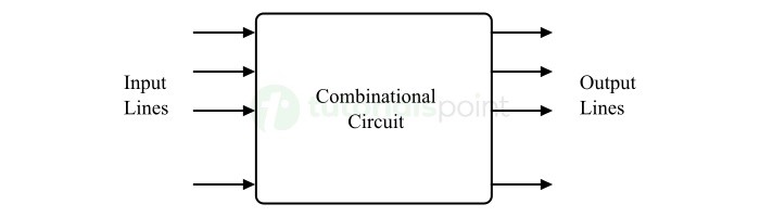
Here, we can see that there are only three key elements in the circuit diagram of a combinational circuit, they are −
- Input Lines − The input lines are used to enter the input values into the combinational circuit.
- Processing Unit − It is the main element that processes the input values depending on the type of the circuit. For example, a full adder adds three binary bits.
- Output Lines − The output lines are used to take results generated by the circuit.
Characteristics of Combinational Circuits
The following are the main characteristics of combinational circuits −
- The output of a combinational circuit, at any instant of time, depends only on the present input values at that instant of time.
- Combinational circuits do not use any kind of memory element in their circuits. Thus, the previous state of input and output values do not have any effect on the present operation of the circuit.
- The output of a combinational circuit can be entirely predicted using its logical operation and input values.
- Combinational circuits produce an instantaneous output in response to any change in its input values.
Types of Combinational Circuits
In digital electronics, the combinational circuits are important components of digital systems. Depending on the functions performed, there are various types of combinational circuits. Some common types of combinational circuits and their functions are explained below −
- Binary Adders
- Binary Subtractors
- Multiplexers (MUX)
- Demultiplexers (DEMUX)
- Encoders
- Decoders
- Comparators
In the following sections of this chapter, we will discuss briefly about each of these combinational circuits along with their functions.
Binary Adders
A binary adder is a combinational circuit that performs the addition of binary digits or bits. Depending on the design and configuration, there are two types of binary adders namely, Half Adder and Full Adder.
Half Adder
The half adder is a combinational logic circuit with two inputs and two outputs. The half adder circuit is designed to add two single-bit binary numbers A and B. It is the basic building block for the addition of two single-bit numbers. This circuit has two outputs namely, sum and carry.
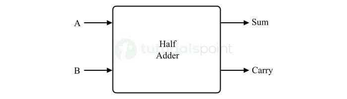
Full Adder
The full adder is designed to overcome the drawback of a half adder which is the ability to add only two bits. Therefore, the full adder is a three-input and two-output combinational circuit. Where, the inputs are two one-bit numbers A and B, and a carry C from the previous addition. The outputs are sum and carry output.
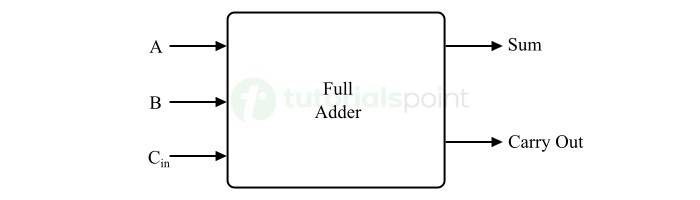
Binary Subtractors
A binary subtractor is a combinational logic circuit used to subtract one binary number from another. Similar to binary adder, there are two types of binary subtractors namely, half-subtractor and full-subtractor.
Half Subtractor
A half subtractor is a combination circuit with two inputs (A and B) and two outputs (difference and borrow). It produces the difference between the two binary bits at the input and also produces an output (Borrow) to indicate if a 1 has been borrowed. In binary subtraction (A-B), A is called a Minuend bit and B is called a Subtrahend bit.

Full Subtractor
The full subtractor is also a combinational circuit with three inputs A, B, and Bin, and two outputs D and Bout.
Here, A is the minuend bit, B is the subtrahend bit, Bin is the previous borrow bit produced by the previous stage, D is the difference output and Bout is the borrow output.
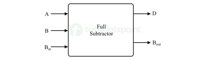
Multiplexers (MUX)
A multiplexer is a special type of combinational logic circuit. It consists of n-data input lines, one output, and m-select lines. For a multiplexer, n = 2m.

A multiplexer is a digital circuit that selects one of the n data inputs and routes it to the output line. The selection of one of the n data inputs is done by the select lines. Depending on the digital code applied at the select lines, one out of "n" data inputs is selected and transmitted to the output line.
In some multiplexers, there is also an enable input E which is useful in cascading of multiple multiplexers.
Depending on the number of input lines, there can be several types of multiplexers. Some common types of multiplexers include 2:1 Multiplexer, 4:1 Multiplexer, 16:1 Multiplexer, and 32:1 Multiplexer.
Demultiplexers (DEMUX)
A demultiplexer performs a distribution operation i.e., it receives one data input and distributes it over several output lines.

A demultiplexer has only one input line, "n" output lines, and "m" select lines. At a time, only one output line is selected by the digital code applied to the select lines and the data input is transmitted to the selected output line.
Demultiplexers can be classified into various types depending on the number of output lines. Some commonly used types of demultiplexers include: 1:2 Demultiplexer, 1:4 Demultiplexer, 1:16 Demultiplexer, and 1:32 Demultiplexer.
Encoders
An encoder is a combinational circuit that is designed to convert a piece of information into a binary code. An encoder has n number of input lines and m number of output lines, where n = 2m.
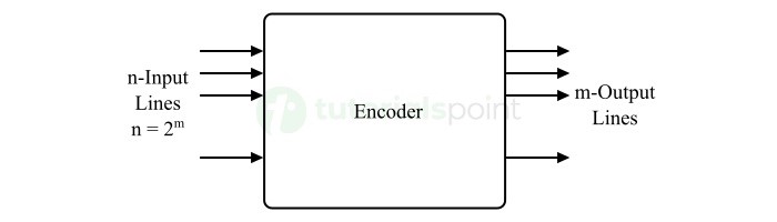
An encoder generates an m-bit binary code corresponding to the digital input applied to it. In other words, an encoder accepts an n-input digital word and converts it into an m-bit another digital word.
Examples of encoder include 4-to-2 encoder, octal-to-binary encoder, hexadecimal-to-binary encoder, priority encoder, etc.
Decoders
A decoder is a combinational circuit that converts a binary code into a normal word like a decimal digit. A decoder typically consists of n input lines and m output lines, where the m = 2n.
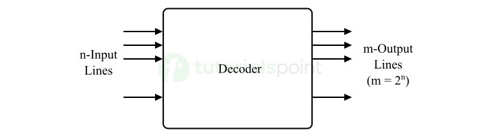
Decoders are widely used in display drivers, data distribution systems, etc.
Some of the commonly used types of decoders are 2 to 4 decoder, 3 to 8 decoder, 4 to 16 decoder, BCD to seven segment decoder, etc.
Comparators
A comparator is a combinational logic circuit developed to compare two binary numbers. Comparators are mainly used in arithmetic and control circuits to perform comparison or logical operations.
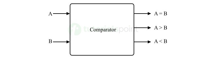
A comparator, as its name suggests, compares the input values and checks whether they are equal or one input is greater/less than the other input.
Limitations of Combinational Circuits
Combinational circuits have several advantages such as fast operational speed, simpler circuit, predictable operation, etc. However, they do have several limitations too, some of which are listed below −
- Combinational circuits do not have any memory element. They are incapable to store history of circuit operation.
- Combinational circuits cannot be used to implement certain highly complex logic functions.
- Combinational circuits do not have any feedback mechanism. That makes the combinational circuits to have limited functionality.
- At large scale, combinational circuits have several design complexities that can result in poor performance and inefficient resource utilization.
Applications of Combinational Circuits
Combinational circuits are the fundamental building blocks in various digital devices and systems. They are widely used in several digital devices in which combinational circuits are used −
- Microprocessors and Microcontrollers
- Digital Computers
- Calculators
- Digital Communication Systems
- Keyboards
- Smartphones and Digital Watches, etc
Conclusion
A combinational logic circuit is a key component in various digital devices and systems. It can be defined as an interconnected system of digital components whose output depends only on the present states of inputs and it does not depend on past input and output values.
In this chapter, we explained the characteristics, limitations, and applications of combinational circuits.
Digital Arithmetic Circuits
In this chapter, let us discuss about the basic arithmetic circuits like Binary adder and Binary subtractor. These circuits can be operated with binary values 0 and 1.
Binary Adder
The most basic arithmetic operation is addition. The circuit, which performs the addition of two binary numbers is known as Binary adder. First, let us implement an adder, which performs the addition of two bits.
Half Adder
Half adder is a combinational circuit, which performs the addition of two binary numbers A and B are of single bit. It produces two outputs sum, S & carry, C.
The Truth table of Half adder is shown below.
| Inputs | Outputs | ||
|---|---|---|---|
| A | B | C | S |
| 0 | 0 | 0 | 0 |
| 0 | 1 | 0 | 1 |
| 1 | 0 | 0 | 1 |
| 1 | 1 | 1 | 0 |
When we do the addition of two bits, the resultant sum can have the values ranging from 0 to 2 in decimal. We can represent the decimal digits 0 and 1 with single bit in binary. But, we cant represent decimal digit 2 with single bit in binary. So, we require two bits for representing it in binary.
Let, sum, S is the Least significant bit and carry, C is the Most significant bit of the resultant sum. For first three combinations of inputs, carry, C is zero and the value of S will be either zero or one based on the number of ones present at the inputs. But, for last combination of inputs, carry, C is one and sum, S is zero, since the resultant sum is two.
From Truth table, we can directly write the Boolean functions for each output as
$$\mathrm{S \: = \: A \: \oplus \: B}$$
$$\mathrm{C \: = \: AB}$$
We can implement the above functions with 2-input Ex-OR gate & 2-input AND gate. The circuit diagram of Half adder is shown in the following figure.

In the above circuit, a two input Ex-OR gate & two input AND gate produces sum, S & carry, C respectively. Therefore, Half-adder performs the addition of two bits.
Full Adder
Full adder is a combinational circuit, which performs the addition of three bits A, B and Cin. Where, A & B are the two parallel significant bits and Cin is the carry bit, which is generated from previous stage. This Full adder also produces two outputs sum, S & carry, Cout, which are similar to Half adder.
The Truth table of Full adder is shown below.
| Inputs | Outputs | |||
|---|---|---|---|---|
| A | B | Cin | Cout | S |
| 0 | 0 | 0 | 0 | 0 |
| 0 | 0 | 1 | 0 | 1 |
| 0 | 1 | 0 | 0 | 1 |
| 0 | 1 | 1 | 1 | 0 |
| 1 | 0 | 0 | 0 | 1 |
| 1 | 0 | 1 | 1 | 0 |
| 1 | 1 | 0 | 1 | 0 |
| 1 | 1 | 1 | 1 | 1 |
When we do the addition of three bits, the resultant sum can have the values ranging from 0 to 3 in decimal. We can represent the decimal digits 0 and 1 with single bit in binary. But, we cant represent the decimal digits 2 and 3 with single bit in binary. So, we require two bits for representing those two decimal digits in binary.
Let, sum, S is the Least significant bit and carry, Cout is the Most significant bit of resultant sum. It is easy to fill the values of outputs for all combinations of inputs in the truth table. Just count the number of ones present at the inputs and write the equivalent binary number at outputs. If Cin is equal to zero, then Full adder truth table is same as that of Half adder truth table.
We will get the following Boolean functions for each output after simplification.
$$\mathrm{S \: = \: A \: \oplus \: B \: \oplus \: C_{in}}$$
$$\mathrm{c_{out} \: = \: AB \: + \: \left ( A \: \oplus \: B \right ) \: c_{in}}$$
The sum, S is equal to one, when odd number of ones present at the inputs. We know that Ex-OR gate produces an output, which is an odd function. So, we can use either two 2input Ex-OR gates or one 3-input Ex-OR gate in order to produce sum, S. We can implement carry, Cout using two 2-input AND gates & one OR gate. The circuit diagram of Full adder is shown in the following figure.

This adder is called as Full adder because for implementing one Full adder, we require two Half adders and one OR gate. If Cin is zero, then Full adder becomes Half adder. We can verify it easily from the above circuit diagram or from the Boolean functions of outputs of Full adder.
4-bit Binary Adder
The 4-bit binary adder performs the addition of two 4-bit numbers. Let the 4-bit binary numbers, $\mathrm{A \: = \: A_{3}A_{2}A_{1}A_{0}}$ and $\mathrm{B \: = \: B_{3}B_{2}B_{1}B_{0}}$. We can implement 4-bit binary adder in one of the two following ways.
- Use one Half adder for doing the addition of two Least significant bits and three Full adders for doing the addition of three higher significant bits.
- Use four Full adders for uniformity. Since, initial carry Cin is zero, the Full adder which is used for adding the least significant bits becomes Half adder.
For the time being, we considered second approach. The block diagram of 4-bit binary adder is shown in the following figure.
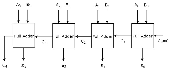
Here, the 4 Full adders are cascaded. Each Full adder is getting the respective bits of two parallel inputs A & B. The carry output of one Full adder will be the carry input of subsequent higher order Full adder. This 4-bit binary adder produces the resultant sum having at most 5 bits. So, carry out of last stage Full adder will be the MSB.
In this way, we can implement any higher order binary adder just by cascading the required number of Full adders. This binary adder is also called as ripple carry (binary) adder because the carry propagates (ripples) from one stage to the next stage.
Binary Subtractor
The circuit, which performs the subtraction of two binary numbers is known as Binary subtractor. We can implement Binary subtractor in following two methods.
- Cascade Full subtractors
- 2s complement method
In first method, we will get an n-bit binary subtractor by cascading 'n' Full subtractors. So, first you can implement Half subtractor and Full subtractor, similar to Half adder & Full adder. Then, you can implement an n-bit binary subtractor, by cascading n Full subtractors. So, we will be having two separate circuits for binary addition and subtraction of two binary numbers.
In second method, we can use same binary adder for subtracting two binary numbers just by doing some modifications in the second input. So, internally binary addition operation takes place but, the output is resultant subtraction.
We know that the subtraction of two binary numbers A & B can be written as,
$$\mathrm{A-B \: = \: A \: + \: \left ( {2}'s \: compliment \: of \: B \right )}$$
$$\mathrm{\Rightarrow \: A \: - \: B \: = \: A \: + \: \left ( {1}'s \: compliment \: of \: B \right ) \: + \: 1}$$
4-bit Binary Subtractor
The 4-bit binary subtractor produces the subtraction of two 4-bit numbers. Let the 4bit binary numbers, $\mathrm{A \: = \: A_{3}A_{2}A_{1}A_{0}}$ and $\mathrm{B \: = \: B_{3}B_{2}B_{1}B_{0}}$. Internally, the operation of 4-bit Binary subtractor is similar to that of 4-bit Binary adder. If the normal bits of binary number A, complemented bits of binary number B and initial carry (borrow), Cin as one are applied to 4-bit Binary adder, then it becomes 4-bit Binary subtractor. The block diagram of 4-bit binary subtractor is shown in the following figure.

This 4-bit binary subtractor produces an output, which is having at most 5 bits. If Binary number A is greater than Binary number B, then MSB of the output is zero and the remaining bits hold the magnitude of A-B. If Binary number A is less than Binary number B, then MSB of the output is one. So, take the 2s complement of output in order to get the magnitude of A-B.
In this way, we can implement any higher order binary subtractor just by cascading the required number of Full adders with necessary modifications.
Binary Adder / Subtractor
The circuit, which can be used to perform either addition or subtraction of two binary numbers at any time is known as Binary Adder / subtractor. Both, Binary adder and Binary subtractor contain a set of Full adders, which are cascaded. The input bits of binary number A are directly applied in both Binary adder and Binary subtractor.
There are two differences in the inputs of Full adders that are present in Binary adder and Binary subtractor.
- The input bits of binary number B are directly applied to Full adders in Binary adder, whereas the complemented bits of binary number B are applied to Full adders in Binary subtractor.
- The initial carry, C0 = 0 is applied in 4-bit Binary adder, whereas the initial carry (borrow), C0 = 1 is applied in 4-bit Binary subtractor.
We know that a 2-input Ex-OR gate produces an output, which is same as that of first input when other input is zero. Similarly, it produces an output, which is complement of first input when other input is one.
Therefore, we can apply the input bits of binary number B, to 2-input Ex-OR gates. The other input to all these Ex-OR gates is C0. So, based on the value of C0, the Ex-OR gates produce either the normal or complemented bits of binary number B.
4-bit Binary Adder / Subtractor
The 4-bit binary adder / subtractor produces either the addition or the subtraction of two 4-bit numbers based on the value of initial carry or borrow, 0. Let the 4-bit binary numbers, $\mathrm{A \: = \: A_{3}A_{2}A_{1}A_{0}}$ and $\mathrm{B \: = \: B_{3}B_{2}B_{1}B_{0}}$. The operation of 4-bit Binary adder / subtractor is similar to that of 4-bit Binary adder and 4-bit Binary subtractor.
Apply the normal bits of binary numbers A and B & initial carry or borrow, C0 from externally to a 4-bit binary adder. The block diagram of 4-bit binary adder / subtractor is shown in the following figure.

If initial carry, 0 is zero, then each full adder gets the normal bits of binary numbers A & B. So, the 4-bit binary adder / subtractor produces an output, which is the addition of two binary numbers A & B.
If initial borrow, 0 is one, then each full adder gets the normal bits of binary number A & complemented bits of binary number B. So, the 4-bit binary adder / subtractor produces an output, which is the subtraction of two binary numbers A & B.
Therefore, with the help of additional Ex-OR gates, the same circuit can be used for both addition and subtraction of two binary numbers.
Digital Electronics - Multiplexers
A digital logic circuit that accepts several data inputs and allows only one of them at a time to flow through the output is called a multiplexer or MUX. This article is meant for explaining multiplexer in digital electronics, its block diagram, function, and different types. So, let us start with the basic introduction of multiplexer
What is a Multiplexer?
As already mentioned, a multiplexer, also referred to as MUX, is a combination logic circuit that is designed to accept multiple input signals and transfer only one of them through the output line. In simple words, a multiplexer is a digital logic device that selects one-out-of-N (N = 2n) input data sources and transmits the selected data to a single output line.
The multiplexer is also called data selector as it selects one from several. The block diagram of a typical 2n:1 multiplexer is shown in Figure 1.

In the case of multiplexer, the selection of desired data input to flow through the output line is controlled with the help of SELECT lines. In the block diagram of mux in Figure 1, I0, I1,... In-1, i.e., (2n) are the input lines, and "n" be the select lines. These select lines will determine which input is to be routed to the output.
Hence, the multiplexer works as a multi-position switch whose operation is controlled by digital signals. These digital control signals are applied to the select lines to determine which data input will be switched to the output line.
Function of Multiplexer
Multiplexer is a digital logic device which is used to perform multiplexing of data. Where, multiplexing simply means sharing of data. Technically, when a particular data is selected from multiple input data sources and transmitted the selected data to a single output channel, it is called multiplexing.
There are two types of multiplexing namely, frequency multiplexing and time multiplexing.
When multiple devices are connected to a single transmission line in a system. At any point of time, only one device is using the line to transmit data, then this is called time multiplexing. On the other hand, when multiple devices share a common line to transmit data but at different frequencies, it is called frequency multiplexing.
Types of Multiplexers
Based on input data lines and select lines, the multiplexer can be of several types. But, in this article, we will discuss only the following three types of multiplexers −
- 2×1 Multiplexer
- 4×1 Multiplexer
Let us discuss each of these three multiplexers individually.
2×1 Multiplexer
The block diagram of a 2×1 multiplexer is shown in Figure 2. The 2×1 multiplexer is basic two input multiplexer which has two data input lines designated as I0 and I1, one data select line denoted by S and one output line denoted by Y. The 2×1 mux is used to connect two 1-bit data sources to a common designation.

In the 2×1 multiplexer, the logic level of the digital signal applied to the select line S determines which data input will pass through the output line. The operation of the 2×1 multiplexer can be understood from the following truth table.
| Select Line (S) | Output (Y) |
|---|---|
| 0 | I0 |
| 1 | I1 |
4×1 Multiplexer
4×1 Multiplexer has four data inputs I3, I2, I1 & I0, two selection lines s1 & s0 and one output Y. The block diagram of 4×1 Multiplexer is shown in the following figure.

One of these 4 inputs will be connected to the output based on the combination of inputs present at these two selection lines. Truth table of 4×1 Multiplexer is shown below.
| Selection Lines | Output | |
|---|---|---|
| S1 | S0 | Y |
| 0 | 0 | I0 |
| 0 | 1 | I1 |
| 1 | 0 | I2 |
| 1 | 1 | I3 |
From Truth table, we can directly write the Boolean function for output, Y as
$$\mathrm{Y\:=\:{S_{1}}'{S_{0}}'I_{0}\:+\:{S_{1}}'S_{0}I_{1}\:+\:S_{1}{S_{0}}'I_{2}\:+\:S_{1}S_{0}I_{3}}$$
We can implement this Boolean function using Inverters, AND gates & OR gate. The circuit diagram of 4×1 multiplexer is shown in the following figure.

We can easily understand the operation of the above circuit. Similarly, you can implement 8×1 Multiplexer and 16×1 multiplexer by following the same procedure.
Implementation of Higher-order Multiplexers
Now, let us implement the following two higher-order Multiplexers using lower-order Multiplexers.
- 8×1 Multiplexer
- 16×1 Multiplexer
8×1 Multiplexer
In this section, let us implement 8×1 Multiplexer using 4×1 Multiplexers and 2×1 Multiplexer. We know that 4×1 Multiplexer has 4 data inputs, 2 selection lines and one output. Whereas, 8×1 Multiplexer has 8 data inputs, 3 selection lines and one output.
So, we require two 4×1 Multiplexers in first stage in order to get the 8 data inputs. Since, each 4×1 Multiplexer produces one output, we require a 2×1 Multiplexer in second stage by considering the outputs of first stage as inputs and to produce the final output.
Let the 8×1 Multiplexer has eight data inputs I7 to I0, three selection lines s2, s1 & s0 and one output Y. The Truth table of 8×1 Multiplexer is shown below.
| Selection Inputs | Output | ||
|---|---|---|---|
| S2 | S1 | S0 | Y |
| 0 | 0 | 0 | I0 |
| 0 | 0 | 1 | I1 |
| 0 | 1 | 0 | I2 |
| 0 | 1 | 1 | I3 |
| 1 | 0 | 0 | I4 |
| 1 | 0 | 1 | I5 |
| 1 | 1 | 0 | I6 |
| 1 | 1 | 1 | I7 |
We can implement 8×1 Multiplexer using lower order Multiplexers easily by considering the above Truth table. The block diagram of 8×1 Multiplexer is shown in the following figure.

The same selection lines, s1 & s0 are applied to both 4×1 Multiplexers. The data inputs of upper 4×1 Multiplexer are I7 to I4 and the data inputs of lower 4×1 Multiplexer are I3 to I0. Therefore, each 4×1 Multiplexer produces an output based on the values of selection lines, s1 & s0.
The outputs of first stage 4×1 Multiplexers are applied as inputs of 2×1 Multiplexer that is present in second stage. The other selection line, s2 is applied to 2×1 Multiplexer.
If s2 is zero, then the output of 2×1 Multiplexer will be one of the 4 inputs I3 to I0 based on the values of selection lines s1 & s0.
If s2 is one, then the output of 2×1 Multiplexer will be one of the 4 inputs I7 to I4 based on the values of selection lines s1 & s0.
Therefore, the overall combination of two 4×1 Multiplexers and one 2×1 Multiplexer performs as one 8×1 Multiplexer.
16×1 Multiplexer
In this section, let us implement 16×1 Multiplexer using 8×1 Multiplexers and 2×1 Multiplexer. We know that 8×1 Multiplexer has 8 data inputs, 3 selection lines and one output. Whereas, 16×1 Multiplexer has 16 data inputs, 4 selection lines and one output.
So, we require two 8×1 Multiplexers in first stage in order to get the 16 data inputs. Since, each 8×1 Multiplexer produces one output, we require a 2×1 Multiplexer in second stage by considering the outputs of first stage as inputs and to produce the final output.
Let the 16×1 Multiplexer has sixteen data inputs I15 to I0, four selection lines s3 to s0 and one output Y. The Truth table of 16×1 Multiplexer is shown below.
| Selection Inputs | Output | |||
|---|---|---|---|---|
| S3 | S2 | S1 | S0 | Y |
| 0 | 0 | 0 | 0 | I0 |
| 0 | 0 | 0 | 1 | I1 |
| 0 | 0 | 1 | 0 | I2 |
| 0 | 0 | 1 | 1 | I3 |
| 0 | 1 | 0 | 0 | I4 |
| 0 | 1 | 0 | 1 | I5 |
| 0 | 1 | 1 | 0 | I6 |
| 0 | 1 | 1 | 1 | I7 |
| 1 | 0 | 0 | 0 | I8 |
| 1 | 0 | 0 | 1 | I9 |
| 1 | 0 | 1 | 0 | I10 |
| 1 | 0 | 1 | 1 | I11 |
| 1 | 1 | 0 | 0 | I12 |
| 1 | 1 | 0 | 1 | I13 |
| 1 | 1 | 1 | 0 | I14 |
| 1 | 1 | 1 | 1 | I15 |
We can implement 16×1 Multiplexer using lower order Multiplexers easily by considering the above Truth table. The block diagram of 16×1 Multiplexer is shown in the following figure.

The same selection lines, s2, s1 & s0 are applied to both 8×1 Multiplexers. The data inputs of upper 8×1 Multiplexer are I15 to I8 and the data inputs of lower 8×1 Multiplexer are I7 to I0. Therefore, each 8×1 Multiplexer produces an output based on the values of selection lines, s2, s1 & s0.
The outputs of first stage 8×1 Multiplexers are applied as inputs of 2×1 Multiplexer that is present in second stage. The other selection line, s3 is applied to 2×1 Multiplexer.
If s3 is zero, then the output of 2×1 Multiplexer will be one of the 8 inputs Is7 to I0 based on the values of selection lines s2, s1 & s0.
If s3 is one, then the output of 2×1 Multiplexer will be one of the 8 inputs I15 to I8 based on the values of selection lines s2, s1 & s0.
Therefore, the overall combination of two 8×1 Multiplexers and one 2×1 Multiplexer performs as one 16×1 Multiplexer.
Applications of Multiplexers
In digital electronics, multiplexers have numerous applications in almost all types of digital systems. Some important applications of multiplexers are as follows −
- Data routing and data selection
- Parallel to series conversion
- Logic function implementation
- Generation of waveform, etc.
Conclusion
In this tutorial, we discussed in detail the different types of multiplexers used in digital electronics along with their functions and applications.
Parity Bit Generator and Checker
In the field of digital electronics, it is very important to ensure the data integrity. For this purpose, we have two digital circuits namely, parity generator and parity checker. Both these circuits help us to detect and correct any kind of error in transmitted data.
Read this chapter to learn the basics of parity generator and parity checker, along with their types and applications.
What is a Parity Bit?
In digital signal processing, an additional bit either 0 or 1 is added to the original binary or digital code to detect and correct any kind of errors in the data that can occur during transmission. This additional bit is called a parity bit.
The addition of a parity bit to the original digital code makes the total number of 1s in the code either even or odd. Thus, on the basis of number 1s in the data, the parity can be classified into two types namely, even parity and odd parity.
If we add a 0 or a 1 to the original binary code and this makes the total number of 1s in the code an even number, then it is called an even parity.
On the other hand, if we add a parity bit i.e., 0 or 1 to the original binary code and this makes the total number of 1s in the code an odd number, then it is called an odd parity.
The parity bit is one of the simplest forms of error-detection technique used in digital electronics.
How Does the Parity Bit Work?
Let us now consider an example to understand how the parity bit works.
Suppose we have a decimal number say 5 and its BCD code is 0101. This code has total number of 1s are even, as it has two 1s.
In the case of even parity, we add a parity bit 0 to the original code to make the number of 1s an even number in the code.
Therefore, after adding even parity, we get 01010. Here, a 0 (parity bit) is added to the end of the original code.
In case, when we need to perform odd parity, then we add a 1 to end of the original code, we get 01011. Now, the total number of 1s in the code, including parity bit, is odd i.e., three 1s. This ensures that it is odd parity scheme.
The following table shows the odd and even parity bits for decimal digits from 0 to 9 −
| Decimal Digit | BCD | Even Parity | Odd Parity |
|---|---|---|---|
| 0 | 0 0 0 0 | 0 | 1 |
| 1 | 0 0 0 1 | 1 | 0 |
| 2 | 0 0 1 0 | 1 | 0 |
| 3 | 0 0 1 1 | 0 | 1 |
| 4 | 0 1 0 0 | 1 | 0 |
| 5 | 0 1 0 1 | 0 | 1 |
| 6 | 0 1 1 0 | 0 | 1 |
| 7 | 0 1 1 1 | 1 | 0 |
| 8 | 1 0 0 0 | 1 | 0 |
| 9 | 1 0 0 1 | 0 | 1 |
When a digital signal is received at the receiver end, a parity checker circuit generates an error signal if the total number of 1s is an odd number in an even parity scheme or an even number in an odd parity scheme.
The major limitation of parity bit error detection technique is that it can check only a single-bit error, but cannot check a multi bit error.
What is a Parity Generator?
A combinational logic circuit that can generate the parity bit according to the original digital code is known as a parity bit generator or parity generator.
The parity generator is used at the transmitter end and generate and add a parity bit the original code before transmission.
First, a parity generator reads the input data and calculates the parity bit accordingly. Once the parity bit is generated, it is added to the original data code. This gives an output code which is the original code with a newly generated parity bit.
Types of Parity Generators
Depending on the parity system used, there are two main types of parity generators −
- Even Parity Generator
- Odd Parity Generator
Let us discuss about even and odd parity generators in detail.
Even Parity Generator
An even parity generator is a type of parity generator in which the parity bit, either a 0 or a 1 is added to the original data so that the final digital code contains an even number of 1s, including the parity bit.
Therefore, we can state that total number of 1s in the output of an even parity generator including the parity bit is even.
In the case of an even parity generator −
- If a digital code contains an odd number of 1s, then the even parity generator will generate a 1 as parity bit to maintain the even parity.
- If a digital code already contains an even number of 1s, then the even parity generator will generate a 0 as the parity bit to maintain the even parity.
For example, consider a digital code 0110. This code already contains the even number of 1s. Hence, if it is input to an even parity generator, the output of the parity generator will be 01100. Where, the LSB 0 is a parity bit added by the even parity generator.
Similarly, consider another digital code 0111. In this case, the total number of 1s in the code is three (odd). If we input this code to an even parity generator, the generators output will be 01111, containing even number of 1s. Where, the LSB 1 is the parity bit.
Let us now design a 4-bit even parity generator. The following is the truth table of the 4-bit even parity generator −
| 4-Bit Code | Even Parity | |||
|---|---|---|---|---|
| A | B | C | D | P |
| 0 | 0 | 0 | 0 | 0 |
| 0 | 0 | 0 | 1 | 1 |
| 0 | 0 | 1 | 0 | 1 |
| 0 | 0 | 1 | 1 | 0 |
| 0 | 1 | 0 | 0 | 1 |
| 0 | 1 | 0 | 1 | 0 |
| 0 | 1 | 1 | 0 | 0 |
| 0 | 1 | 1 | 1 | 1 |
| 1 | 0 | 0 | 0 | 1 |
| 1 | 0 | 0 | 1 | 0 |
| 1 | 0 | 1 | 0 | 0 |
| 1 | 0 | 1 | 1 | 1 |
| 1 | 1 | 0 | 0 | 0 |
| 1 | 1 | 0 | 1 | 1 |
| 1 | 1 | 1 | 0 | 1 |
| 1 | 1 | 1 | 1 | 0 |
The Boolean expression of the 4-bit even parity generator can be obtained by simplifying its truth table, which is given below.
$$\mathrm{P \: = \: A \: \oplus \: B \: \oplus \: C \: \oplus \: D}$$
The logic circuit diagram of a 4-bit even parity generator is shown in the following figure.
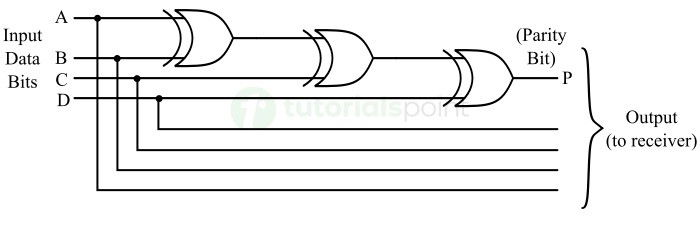
In this circuit, three XOR gates are connected together to add four data bits of the input code. The sum bit produced at the output will be the parity bit.
This is all about the even parity generator and its functioning.
Odd Parity Generator
A type of parity generator that adds a parity bit to a binary code so that the total number of 1s in the output code is an odd number, it is called an odd parity generator.
The output of an odd parity generator is a digital code that contains an odd number of 1s, including the parity bit.
In the case of an odd parity generator,
- If the original data contains an even number of 1s, then the odd parity generator adds a 1 as parity bit to the original code to maintain the odd parity.
- If the original data already contains an odd number of 1s, then the odd parity generator adds a 0 as parity bit to the original code to maintain the odd parity.
Let us understand the function of the odd parity generator with the help of examples.
Consider a 4-bit digital code that is 0110. This code has even number of 1s (two). Therefore, if we input this code to an odd parity generator, the generator will add a 1 and produces a code 01101 as output. This resulting code has odd number of 1s, including the parity bit, and ensuring the odd parity system.
Similarly, consider another 4-bit code that is 0111. This code already contains odd number of 1s i.e., three 1s. Therefore, the odd parity generator will add a 0 as parity bit to it and gives an output code as 01110 to ensure the odd parity system.
The following is the truth table of a 4-bit odd parity generator −
| 4-Bit Code | Odd Parity | |||
|---|---|---|---|---|
| A | B | C | D | P |
| 0 | 0 | 0 | 0 | 1 |
| 0 | 0 | 0 | 1 | 0 |
| 0 | 0 | 1 | 0 | 0 |
| 0 | 0 | 1 | 1 | 1 |
| 0 | 1 | 0 | 0 | 0 |
| 0 | 1 | 0 | 1 | 1 |
| 0 | 1 | 1 | 0 | 1 |
| 0 | 1 | 1 | 1 | 0 |
| 1 | 0 | 0 | 0 | 0 |
| 1 | 0 | 0 | 1 | 1 |
| 1 | 0 | 1 | 0 | 1 |
| 1 | 0 | 1 | 1 | 0 |
| 1 | 1 | 0 | 0 | 1 |
| 1 | 1 | 0 | 1 | 0 |
| 1 | 1 | 1 | 0 | 0 |
| 1 | 1 | 1 | 1 | 1 |
The Boolean expression of the 4-bit odd parity generator is,
$$\mathrm{P \: = \: \overline{A \: \oplus \: B \: \oplus \: C \: \oplus \: D}}$$
The following figure depicts the logic circuit diagram of the 4-bit odd parity generator.

In this circuit, three XOR gates are connected together to add the four bits of the input data and the sum bit is then complemented to obtain the odd parity bit.
This is all about the even parity generator and odd parity generator. Both of these types of parity generators are used in digital systems to implement different types of parity systems depending on the needs of the applications.
Parity generators are extensively used in digital communication and storage systems to check errors that can occur during transmission of data.
What is a Parity Checker?
A combinational circuit that checks and verifies the correctness of the transmitted data by analyzing the parity bit is called a parity checker. The main function of a parity checker is to detect errors that can occur during data transmission.
Parity checkers are used at the receiver end of the communication channel. It receives the transmitted data from the communication channel. This data includes the original message code and the parity bit.
After that, the parity checker counts the number of 1s in the data code and compares this number with the expected code to determine whether there is any error or not. If there is any error in the received data, the parity checker takes an appropriate action like request to retransmit the data.
The parity checker is an essential component in the digital communication systems to ensure the correctness and integrity of data. It also provides a simple and effective method for error detection.
Types of Parity Checkers
Depending on the parity system used, there are two main types of parity checkers −
- Even Parity Checker
- Odd Parity Checker
Let us discuss each type of parity checker in detail.
Even Parity Checker
The type of parity checker that verifies whether the received data is correct as per the even parity system is called an even parity checker.
The even parity checker counts and verifies that the received data contains an even number of 1s, including the parity bit.
Thus, in the case of an even parity checker,
- If the number of 1s in the received data is even, then it is considered that the data is error free.
- If the number of 1s in the received data is odd, then the parity checker shows that the data contains some error.
How Does an Even Parity Checker Work?
Let us understand the even parity checking with the help of an example.
Consider a 4-bit digital code 00110 (having 0 as parity bit at LSB position), this code is received by the even parity checker. The parity checker will count the number of 1s in the code which is even (two). Thus, the parity checker shows that it is an error free code, where LSB 0 is the parity bit.
Similarly, consider another 4-bit message code 01011 with a parity bit at the LSB place. This code contains odd number of 1s (three 1s). Hence, the even parity checker will show that the code has some error.
Let us now implement a 4-bit even parity checker whose truth table is shown below −
| 4-Bit Code with Parity | Even Parity Check | ||||
|---|---|---|---|---|---|
| A | B | C | D | P | CP |
| 0 | 0 | 0 | 0 | 0 | 0 |
| 0 | 0 | 0 | 0 | 1 | 1 |
| 0 | 0 | 0 | 1 | 0 | 1 |
| 0 | 0 | 0 | 1 | 1 | 0 |
| 0 | 0 | 1 | 0 | 0 | 1 |
| 0 | 0 | 1 | 0 | 1 | 0 |
| 0 | 0 | 1 | 1 | 0 | 0 |
| 0 | 0 | 1 | 1 | 1 | 1 |
| 0 | 1 | 0 | 0 | 0 | 1 |
| 0 | 1 | 0 | 0 | 1 | 0 |
| 0 | 1 | 0 | 1 | 0 | 0 |
| 0 | 1 | 0 | 1 | 1 | 1 |
| 0 | 1 | 1 | 0 | 0 | 0 |
| 0 | 1 | 1 | 0 | 1 | 1 |
| 0 | 1 | 1 | 1 | 0 | 1 |
| 0 | 1 | 1 | 1 | 1 | 0 |
| 1 | 0 | 0 | 0 | 0 | 1 |
| 1 | 0 | 0 | 0 | 1 | 0 |
| 1 | 0 | 0 | 1 | 0 | 0 |
| 1 | 0 | 0 | 1 | 1 | 1 |
| 1 | 0 | 1 | 0 | 0 | 0 |
| 1 | 0 | 1 | 0 | 1 | 1 |
| 1 | 0 | 1 | 1 | 0 | 1 |
| 1 | 0 | 1 | 1 | 1 | 0 |
| 1 | 1 | 0 | 0 | 0 | 0 |
| 1 | 1 | 0 | 0 | 1 | 1 |
| 1 | 1 | 0 | 1 | 0 | 1 |
| 1 | 1 | 0 | 1 | 1 | 0 |
| 1 | 1 | 1 | 0 | 0 | 1 |
| 1 | 1 | 1 | 0 | 1 | 0 |
| 1 | 1 | 1 | 1 | 0 | 0 |
| 1 | 1 | 1 | 1 | 1 | 1 |
Here, the bits ABCD represents the original digital code and P is the parity bit.
In this truth table, if CP = 1, there will be an error in the received code. If CP = 0, there is no error in the received code.
The Boolean expression of the 4-bit even parity checker is,
$$\mathrm{C_{P} \: = \: A \: \oplus \: B \: \oplus \: C \: \oplus \: D \: \oplus \: P}$$
The logic circuit diagram of the 4-bit even parity checker is shown in the following figure.
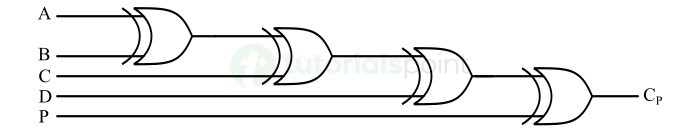
Odd Parity Checker
An odd parity checker is a combinational logic circuit that checks and verifies whether the received data is correct as per the odd parity system.
An odd parity checker counts and confirms that the received data contains odd number of 1s including the parity bit.
In the case of an odd parity checker,
- If the number of 1s in the received code is odd, there is no error in the code.
- If the number of 1s in the received code is even, this represents an error in the code that might be occurred during transmission.
For example, consider a 4-bit data code 01101 (LSB 1 is the parity bit). In this code, the number of 1s are odd (three). Thus, the odd parity checker will show that the code is error free.
Similarly, consider another 4-bit data code 01100 (LSB 0 is the parity bit). This code contains the even number of 1s i.e., only two 1s are there. In this case, the odd parity checker will show that the code has an error.
Let us now implement a 4-bit odd parity checker whose truth table is shown below.
| 4-Bit Code with Parity | Odd Parity Check | ||||
|---|---|---|---|---|---|
| A | B | C | D | P | CP |
| 0 | 0 | 0 | 0 | 0 | 1 |
| 0 | 0 | 0 | 0 | 1 | 0 |
| 0 | 0 | 0 | 1 | 0 | 0 |
| 0 | 0 | 0 | 1 | 1 | 1 |
| 0 | 0 | 1 | 0 | 0 | 0 |
| 0 | 0 | 1 | 0 | 1 | 1 |
| 0 | 0 | 1 | 1 | 0 | 1 |
| 0 | 0 | 1 | 1 | 1 | 0 |
| 0 | 1 | 0 | 0 | 0 | 0 |
| 0 | 1 | 0 | 0 | 1 | 1 |
| 0 | 1 | 0 | 1 | 0 | 1 |
| 0 | 1 | 0 | 1 | 1 | 0 |
| 0 | 1 | 1 | 0 | 0 | 1 |
| 0 | 1 | 1 | 0 | 1 | 0 |
| 0 | 1 | 1 | 1 | 0 | 0 |
| 0 | 1 | 1 | 1 | 1 | 1 |
| 1 | 0 | 0 | 0 | 0 | 0 |
| 1 | 0 | 0 | 0 | 1 | 1 |
| 1 | 0 | 0 | 1 | 0 | 1 |
| 1 | 0 | 0 | 1 | 1 | 0 |
| 1 | 0 | 1 | 0 | 0 | 1 |
| 1 | 0 | 1 | 0 | 1 | 0 |
| 1 | 0 | 1 | 1 | 0 | 0 |
| 1 | 0 | 1 | 1 | 1 | 1 |
| 1 | 1 | 0 | 0 | 0 | 1 |
| 1 | 1 | 0 | 0 | 1 | 0 |
| 1 | 1 | 0 | 1 | 0 | 0 |
| 1 | 1 | 0 | 1 | 1 | 1 |
| 1 | 1 | 1 | 0 | 0 | 0 |
| 1 | 1 | 1 | 0 | 1 | 1 |
| 1 | 1 | 1 | 1 | 0 | 1 |
| 1 | 1 | 1 | 1 | 1 | 0 |
In this truth table, the bits ABCD represents the original binary code and P is the parity bit.
From this truth table, we can observe that if CP = 1, the code contains an even number of 1s and hence, there is an error occurred in the code during transmission.
If CP = 0, the code contains odd number of 1s which represents that the code is error free.
The Boolean expression of the 4-bit odd parity checker is given here,
$$\mathrm{C_{P} \: = \: \overline{A \: \oplus \: B \: \oplus \: C \: \oplus \: D \: \oplus \: P}}$$
The logic circuit diagram of this 4-bit odd parity checker is depicted in the following figure.

IC 74180 9-Bit Parity Generators/Checkers
A parity generator/checker IC is a small device which is used to detect errors in data streams transmitted over a communication channel. There are several different parity generator/checker IC available in the market, but one most commonly used is 74180 IC.
The 74180 Parity Generator/Checker IC is a 9-bit parity generator or checker device that is used in high-speed data transmission systems to detect errors.
The pin diagram of the parity generator/checker IC 74180 is shown in the following figure.

It consists of eight input lines labeled from A to H, two cascading input lines labeled as "even" and "odd", and two output lines designated as "even sum" and "odd sum".
Depending on the operating mode selected, the IC 74180 can operate as either a parity generator or a parity checker.
Let us now consider an example to understand the how does the parity generator/checker IC work?
If the IC 74180 is operated as an even parity checker and there is a parity error in the received data. In this case, the output "even sum" will be low and the output "odd sum" will be high.
If the IC 74180 is operated as an odd parity checker and an error occurs in the data stream. The output "odd sum" will be low and the output "even sum" will be high.
This is all about parity generator or checker IC 74180. Let us now discuss the applications of parity generators/checkers.
Applications of Parity Generators and Checkers
In digital systems, like digital communication and storage systems, the parity generator and checker are essential components that provide a robust method for error detection and correction in transmitted and retrieved data streams. Thus, parity generator/checker helps to ensure data integrity, reliability, and security of digital data.
The following examples illustrate the applications of parity generators and checkers in various digital electronic applications −
- In digital communication systems, parity generators and checkers are used to ensure integrity and accuracy of the transmitted and received data. Parity generators and checkers help to detect errors in the data that can be caused due to noise and interference during transmission over communication channels.
- Parity generators and checkers are used in storage systems like RAM and ROM to detect errors in the data stored and retrieved.
- In digital networking, parity generators and checkers are used to improve reliability of data transmission and verify the correctness of the transmitted data.
- Parity generators and checkers are used in industrial automation and control systems to ensure accurate and reliable operation of industrial systems.
- Parity generators and checkers are also used in medical equipment used to diagnose and monitor patients health and avoid any kind errors in medical reports and diagnosis data.
Conclusion
A parity generator is a combinational logic circuit used to generate and add a parity to the input or transmitted data, while a parity checker is also a combinational circuit used to verify the correctness of received data.
Parity generators are used in the transmitter circuit and parity checkers are used in the receiver circuit. Both these circuits are collectively used to ensure the reliability, integrity, and accuracy of data in various digital systems.
Digital Electronics - Comparators
In digital electronics, a comparator is a combinational logic circuit that is used to compare the magnitudes of two binary numbers. Comparators are used in several different electronic circuits like analog to digital converters, voltage level detectors, zero-crossing detectors, etc.
The most basic example of a comparator is an XNOR gate which produces a high or logic 1 output only when both its inputs are equal.
In this chapter, we will learn about the basics, types, and applications of comparators in digital electronics. So, lets start with the basic definition of a comparator.
What is a Comparator?
A digital combinational circuit used to compare the magnitude of two binary numbers to determine the equality or non-equality is called a comparator.
Therefore, the main function of a comparator is to compare the values of input numbers and produce an output indicating whether the numbers are equal or specifies which of the numbers is greater.
Let us understand the working of a comparator with the help of an example.
Consider two 3-bit binary numbers A2A1A0 and B2B1B0. These two binary numbers are said to be equal if all their corresponding bits coincide. In other words, these two binary numbers are equal if A2 = B2, A1 = B1, and A0 = B0.
The block diagram of a typical comparator is shown in the following figure −
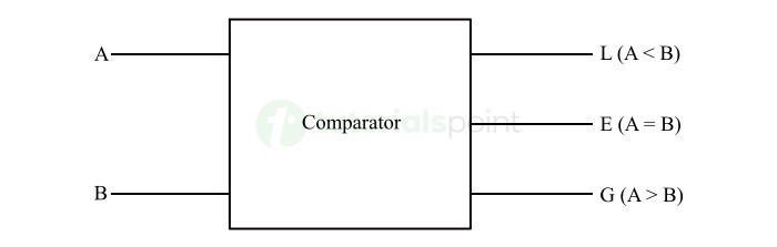
Here, A and B are the input bits, and L, E, and G are the output lines, where L indicates which number is smaller, E indicates equality, and G indicates the greater number.
Types of Comparators
Depending on the number of bits, the following are some main types of comparators used in digital circuits −
- 1-Bit Magnitude Comparator
- 2-Bit Magnitude Comparator
- 4-Bit Magnitude Comparator
Let us discuss each type of comparator in detail.
1-Bit Magnitude Comparator
A 1-bit magnitude comparator is a logic circuit which can compare two binary numbers of one bit each. It produces an output that indicates the relationship between the two input numbers.
In other words, a 1-bit magnitude comparator is one that compares two 1-bit binary numbers and generates an output showing whether one number is equal to or greater than or less than the other.
The block diagram of a 1-bit magnitude comparator is shown in the following figure −
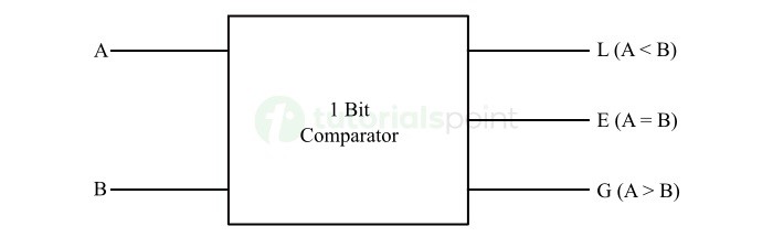
Here, A and B are the 1-bit input numbers, and L, E, and G are the output lines indicating less than or equal to or greater than relationship between A and B respectively.
Let us understand the working this type of comparator.
If A = 0 and B = 0 or if A = 1 and B = 1, then A = B. It indicates that the two binary numbers are equal. Therefore,
$$\mathrm{E \: = \: \overline{A} \: \cdot \: \overline{B} \: + \: A \: \cdot \: B \: = \: A \: \odot \: B}$$
If A = 0 and B = 1, then A < B. This indicates that the binary number A is less than the binary number B. Therefore,
$$\mathrm{L \: = \: \overline{A} \: B}$$
If A = 1 and B = 0, then A > B. It indicates that the binary number A is greater than the binary number B. Therefore,
$$\mathrm{G \: = \: A \: \overline{B}}$$
The 1-bit magnitude comparator compares the corresponding bits of the input numbers A and B. For this, it uses different types of logic gates.
The truth table of the 1-bit magnitude comparators is given below −
| Inputs | Outputs | |||
|---|---|---|---|---|
| A | B | L (A < B) | E (A = B) | G (A > B) |
| 0 | 0 | 0 | 1 | 0 |
| 0 | 1 | 1 | 0 | 0 |
| 1 | 0 | 0 | 0 | 1 |
| 1 | 1 | 0 | 1 | 0 |
We can use this truth table to obtain the Boolean expression of the 1-bit magnitude comparator.
$$\mathrm{L \: = \: \overline{A} \: B}$$
$$\mathrm{E \: = \: \overline{A} \: \cdot \: \overline{B} \: + \: A \: \cdot \: B \: = \: A \: \odot \: B}$$
$$\mathrm{G \: = \: A \: \overline{B}}$$
The logic circuit diagram of the 1-bit magnitude comparator is shown in the following figure.

It consists of two AND gates, two NOT gate, and an XNOR gate.
2-Bit Magnitude Comparator
A digital combinational circuit used to compare the magnitudes of two 2-bit binary numbers and determine the relationship between them is called a 2-bit magnitude comparator.
Hence, the 2-bit magnitude comparator compares the values represented by two 2-bit binary numbers and then generates an output that indicates whether one number is equal to or greater than or less than the other.
The block diagram of a typical 2-bit magnitude comparator is shown in the following figure −
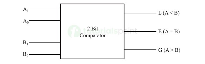
Here, the lines A0A1 and B0B1 represents two 2-bit binary number inputs and the lines L, E, and G represents the less than, equal to, and greater than output lines.
We can understand the operation of the 2-bit magnitude comparator with the help of its truth table given below −
| Inputs | Outputs | |||||
|---|---|---|---|---|---|---|
| A1 | A0 | B1 | B0 | L (A < B) | E (A = B) | G (A > B) |
| 0 | 0 | 0 | 0 | 0 | 1 | 0 |
| 0 | 0 | 0 | 1 | 1 | 0 | 0 |
| 0 | 0 | 1 | 0 | 1 | 0 | 0 |
| 0 | 0 | 1 | 1 | 1 | 0 | 0 |
| 0 | 1 | 0 | 0 | 0 | 0 | 1 |
| 0 | 1 | 0 | 1 | 0 | 1 | 0 |
| 0 | 1 | 1 | 0 | 1 | 0 | 0 |
| 0 | 1 | 1 | 1 | 1 | 0 | 0 |
| 1 | 0 | 0 | 0 | 0 | 0 | 1 |
| 1 | 0 | 0 | 1 | 0 | 0 | 1 |
| 1 | 0 | 1 | 0 | 0 | 1 | 0 |
| 1 | 0 | 1 | 1 | 1 | 0 | 0 |
| 1 | 1 | 0 | 0 | 0 | 0 | 1 |
| 1 | 1 | 0 | 1 | 0 | 0 | 1 |
| 1 | 1 | 1 | 0 | 0 | 0 | 1 |
| 1 | 1 | 1 | 1 | 0 | 1 | 0 |
Let us now derive the Boolean expression for the outputs L, E, and G.
Case 1: A = B
The comparator produces an output A = B which is E, if A0 = B0 and A1 = B1. Therefore, the Boolean expression for the output E will be,
$$\mathrm{E \: = \: (A_{0} \: \odot \: B_{0}) \: (A_{1} \: \odot \: B_{1})}$$
Case 2: A < B
The comparator produces an output A < B which is L, if
- A1 = 0 and B1 = 1, OR
- A1 = B1 and A0 = 0 and B0 = 1.
From these statements, we can write the Boolean expression for the output L as follows −
$$\mathrm{L \: = \: \overline{A_{1}} \: B_{1} \: + \: (A_{1} \: \odot \: B_{1}) \: \overline{A_{0}} \: B_{0}}$$
Case 3: A > B
The output of the comparator will be A > B i.e., G, if
- A1 = 1 and B1 = 0, OR
- A1 = B1 and A0 = 1 and B0 = 0.
From these statements, the Boolean expression for the output G will be,
$$\mathrm{G \: = \: A_{1} \: \overline{B_{1}} \: + \: (A_{1} \: \odot \: B_{1}) \: A_{0} \: \overline{B_{0}}}$$
The following figure shows the logic circuit diagram of the 2-bit magnitude comparator −

4-Bit Magnitude Comparator
The 4-bit magnitude comparator is used in more complex digital circuits like microprocessors, microcontrollers, and many more.
It is a type of comparator that can compare the values or magnitudes of two 4-bit binary numbers and produce an output indicating whether one number is equal to or less than or greater than the other.
The block diagram of the 4-bit magnitude comparator is shown in the following figure −
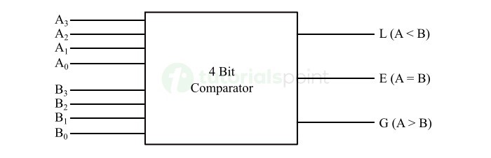
Let us now understand the working of this 4-bit magnitude comparator. For that consider A = A3A2A1A0 is the first 4-bit binary number and B = B3B2B1B0 is the second 4-bit binary number.
The comparator will show the results as follows −
Case 1: A = B
The comparator will produce an output A = B which is E, if all the corresponding bits in the two numbers are equal i.e., A3 = B3 and A2 = B2 and A1 = B1 and A0 = B0.
In this case, the Boolean expression of the output will be,
$$\mathrm{E \: = \: (A_{3} \: \odot \: B_{3}) \: (A_{2} \: \odot \: B_{2}) \: (A_{1} \: \odot \: B_{1}) \: (A_{0} \: \odot \: B_{0})}$$
Case 2: A < B
The comparator will produce an output A < B which is L, if
- A3 = 0 and B3 = 1, OR
- A3 = B3 and if A2 = 0 and B2 = 1, OR
- A3 = B3 and if A2 = B2 and if A1 = 0 and B1 = 1, OR
- A3 = B3 and if A2 = B2 and if A1 = B1 and if A0 = 0 and B0 = 1.
From these statements, we can derive the Boolean expression for the output L, which is given below.
$$\mathrm{L \: = \: \overline{A_{3}} \: B_{3} \: + \: (A_{3} \: \odot \: B_{3}) \: \overline{A_{2}} \: B_{2} \: + \: (A_{3} \: \odot \: B_{3}) \: (A_{2} \: \odot \: B_{2}) \: \overline{A_{1}} \: B_{1} \: + \: (A_{3} \: \odot \: B_{3}) \: (A_{2} \: \odot \: B_{2}) \: (A_{1} \: \odot \: B_{1}) \: \overline{A_{0}} \: B_{0}}$$
Case 3: A > B
The comparator produces an output A > B which is G, if
- A3 = 1 and B3 = 0, OR
- A3 = B3 and if A2 = 1 and B2 = 0, OR
- A3 = B3 and if A2 = B2 and if A1 = 1 and B1 = 0, OR
- A3 = B3 and if A2 = B2 and if A1 = B1 and if A0 = 1 and B0 = 0.
Hence, from these statements, we can write the Boolean expression for the output G which is,
$$\mathrm{G \: = \: A_{3} \: \overline{B_{3}} \: + \: (A_{3} \: \odot \: B_{3}) \: A_{2} \: \overline{B_{2}} \: + \: (A_{3} \: \odot \: B_{3}) \: (A_{2} \: \odot \: B_{2}) \: A_{1} \: \overline{B_{1}} \: + \: (A_{3} \: \odot \: B_{3}) \: (A_{2} \: \odot \: B_{2}) \: (A_{1} \: \odot \: B_{1}) \: A_{0} \: \overline{B_{0}}}$$
The logic circuit implementation of the 4-bit magnitude comparator is shown in the following figure −
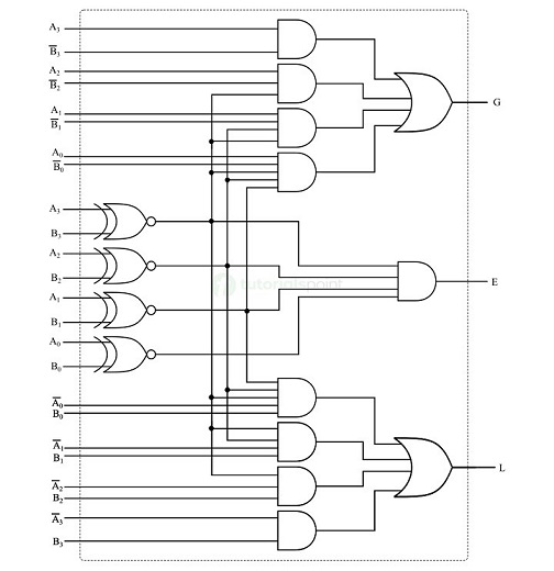
Comparator IC
A comparator IC is an integrated circuit which is designed to compare two binary numbers and produce an output based on the comparison results.
A commonly used comparator IC is IC 7485 which is a 4-bit magnitude comparator IC. It is widely in digital electronic applications to compare two 4-bit binary numbers.
The IC 7485 compares corresponding bits of the two input numbers and determines whether one number is equal to or greater than or less than the other. The pin diagram of the IC 7485 is depicted in the following figure.
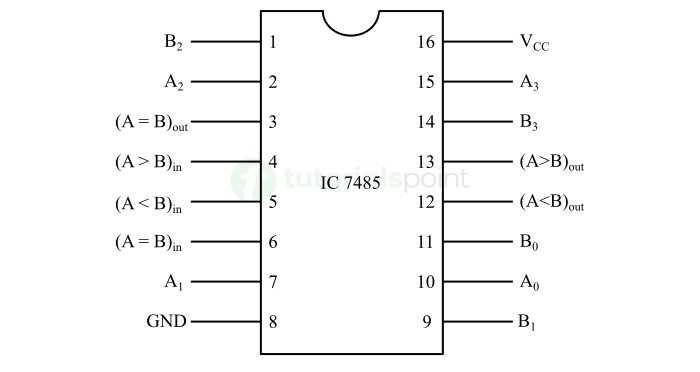
This IC is widely used in various digital circuits such as microprocessors, microcontrollers, control systems, and arithmetic logic units.
Applications of Comparators
The comparators are fundamental components in various digital circuits. They provide capabilities to compare voltage levels and make decisions.
Some of the key applications of comparators in the field of digital electronics are listed below −
- Comparators are used to detect changes in voltage levels in electronic circuits.
- Comparators are also used temperature monitoring systems.
- Comparators are used as zero-crossing detector in various power circuits like phase control circuits, motor and power control circuits, etc.
- Comparators are key components in analog to digital converters (ADCs).
- In signal conditioning circuits, the comparators are used for amplification and filtering of signals before processing.
Conclusion
In conclusion, a comparator is a combinational logic circuit used in various digital electronic applications to compare two similar quantities like two 2-bit binary numbers or two voltage levels, etc.
Comparators help us to make decisions based on a comparison of two input values. They are widely used in several different electronic devices and systems such as arithmetic logic units, microprocessor-based systems, control systems, automation systems, and telecommunication systems.
Depending on the number of input bits required for a particular application, we can design a 1-bit, 2-bit, or 4-bit comparator. Also, comparators are available in the form of integrated circuit. The most commonly used IC comparator is IC 7485 which is a 4-bit magnitude comparator.
Digital Electronics - Encoders
An encoder is a combinational logic circuit that is used to convert a normal or familiar information into a coded format. In other words, an encoder is a digital device that coverts a piece of information represented in the form of decimal digits and alphabetic characters into a coded form like binary representation. The operation that the encoder performs is termed as encoding.
In this chapter, we will explain the basics of encoder and commonly used types of encoders.
What is an Encoder?
An encoder is a digital combinational circuit that converts a human friendly information into a coded format for processing using machines. In simple words, an encoder converts a piece of information normal form to coded form. This process is called encoding.
Encoders are crucial components in various digital electronics applications such as data transmission, controlling and automation, communication, signal processing, etc.
An encoder consists of a certain number of input and output lines. Where, an encoder can have maximum of "2n" input lines whereas "n" output lines. Hence, an encoder encodes information represented by "2n" input lines with "n" bits.
The block diagram of an encoder is shown in the following figure −

Let us now discuss different types of encoders commonly used in digital electronic applications.
Types of Encoders
Some of the commonly used types of encoders in digital electronics −
- 4 to 2 Encoder
- 8 to 3 Encoder (Octal Encoder)
- Decimal to BCD Encoder
Let us now discuss these three types of most commonly used encoders in detail.
4 to 2 Encoder
A 4 to 2 Encoder is a type of encoder which has 4 (22) input lines and 2 output lines. It produces an output code (i.e., convert input information in a 2-bit format) depending on the combination of input lines.
The block diagram of a 4 to 2 Encoder is shown in the following figure.

The working of a 4 to 2 Encoder for different input combinations is described in the following truth table −
| Inputs | Outputs | ||||
|---|---|---|---|---|---|
| I3 | I2 | I1 | I0 | Y1 | Y0 |
| 0 | 0 | 0 | 1 | 0 | 0 |
| 0 | 0 | 1 | 0 | 0 | 1 |
| 0 | 1 | 0 | 0 | 1 | 0 |
| 1 | 0 | 0 | 0 | 1 | 1 |
From this truth table, we can derive the Boolean expression for each output of the 4 to 2 Encoder as follows −
$$\mathrm{Y_{0} \: = \: I_{1} \: + \: I_{3}}$$
$$\mathrm{Y_{1} \: = \: I_{2} \: + \: I_{3}}$$
It is clear that we can implement the logic circuit of the 4 to 2 Encoder using two OR gates. The following figure depicts the logic diagram of the 4 to 2 Encoder.
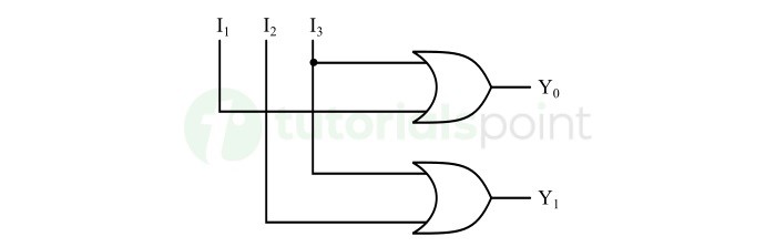
Applications of 4 to 2 Encoder
The 4 to 2 Encoder is widely used in the following applications: Data multiplexing, Generating digital control signals, Address decoding applications, Encoding data in digital systems, etc.
Octal to Binary Encoder
The octal to binary encoder is a type of encoder that converts an octal code into binary code. It accepts 8 input lines and produces a 3-bit output depending on the combination of input lines. Therefore, it is also known as 8 to 3 Encoder.
The block diagram of an octal to binary encoder is shown in the following figure −
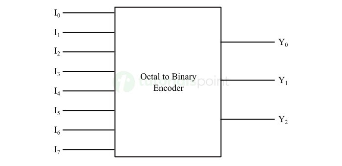
The following truth table describes the working of an octal to binary encoder −
| Inputs | Outputs | |||||||||
|---|---|---|---|---|---|---|---|---|---|---|
| I7 | I6 | I5 | I4 | I3 | I2 | I1 | I0 | Y2 | Y1 | Y0 |
| 0 | 0 | 0 | 0 | 0 | 0 | 0 | 1 | 0 | 0 | 0 |
| 0 | 0 | 0 | 0 | 0 | 0 | 1 | 0 | 0 | 0 | 1 |
| 0 | 0 | 0 | 0 | 0 | 1 | 0 | 0 | 0 | 1 | 0 |
| 0 | 0 | 0 | 0 | 1 | 0 | 0 | 0 | 0 | 1 | 1 |
| 0 | 0 | 0 | 1 | 0 | 0 | 0 | 0 | 1 | 0 | 0 |
| 0 | 0 | 1 | 0 | 0 | 0 | 0 | 0 | 1 | 0 | 1 |
| 0 | 1 | 0 | 0 | 0 | 0 | 0 | 0 | 1 | 1 | 0 |
| 1 | 0 | 0 | 0 | 0 | 0 | 0 | 0 | 1 | 1 | 1 |
From this truth table, we can write the Boolean expression for the outputs of the octal to binary encoder as follows.
$$\mathrm{Y_{0} \: = \: I_{1} \: + \: I_{3} \: + \: I_{5} \: + \: I_{7}}$$
$$\mathrm{Y_{1} \: = \: I_{2} \: + \: I_{3} \: + \: I_{6} \: + \: I_{7}}$$
$$\mathrm{Y_{2} \: = \: I_{4} \: + \: I_{5} \: + \: I_{6} \: + \: I_{7}}$$
From these expressions, it is clear that the implementation of an octal to binary encoder requires 3 OR gates.
The logic circuit diagram of the octal to binary encoder is shown in the following figure −
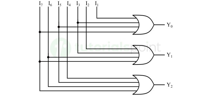
Applications of Octal to Binary Encoder
The octal to binary encoder is used in the following applications −
- Data conversion in digital systems.
- Conversion of octal memory addresses into binary memory addresses.
- In microprocessors and microcontrollers, to convert octal instructions into binary format.
- In communication systems, to encode octal data into binary form for transmission, etc.
Decimal to BCD Encoder
A type of encoder that can convert a decimal number or information represented using decimal number into its equivalent binary-coded decimal (BCD) format is known as a decimal to BCD encoder.
In the BCD encoding scheme, each decimal digit can be converted into a 4-bit binary representation. The following table shows the BCD equivalents of decimal digital from 0 to 9.
| Decimal Digit | BCD Code | |||
|---|---|---|---|---|
| 0 | 0 | 0 | 0 | 0 |
| 1 | 0 | 0 | 0 | 1 |
| 2 | 0 | 0 | 1 | 0 |
| 3 | 0 | 0 | 1 | 1 |
| 4 | 0 | 1 | 0 | 0 |
| 5 | 0 | 1 | 0 | 1 |
| 6 | 0 | 1 | 1 | 0 |
| 7 | 0 | 1 | 1 | 1 |
| 8 | 1 | 0 | 0 | 0 |
| 9 | 1 | 0 | 0 | 1 |
The decimal to BCD encoder accepts 10 input lines and produces a 4-bit BCD output depending on the combination of input lines. Therefore, sometimes it is also called a 10 to 4 encoder.
The following illustration depicts the block diagram of a decimal to BCD encoder.
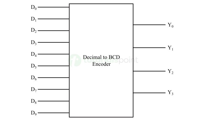
The truth table describing the working of the decimal to BCD encoder is given blow −
| Inputs | Outputs | ||||||||||||
|---|---|---|---|---|---|---|---|---|---|---|---|---|---|
| D9 | D8 | D7 | D6 | D5 | D4 | D3 | D2 | D1 | D0 | Y3 | Y2 | Y1 | Y0 |
| 0 | 0 | 0 | 0 | 0 | 0 | 0 | 0 | 0 | 1 | 0 | 0 | 0 | 0 |
| 0 | 0 | 0 | 0 | 0 | 0 | 0 | 0 | 1 | 0 | 0 | 0 | 0 | 1 |
| 0 | 0 | 0 | 0 | 0 | 0 | 0 | 1 | 0 | 0 | 0 | 0 | 1 | 0 |
| 0 | 0 | 0 | 0 | 0 | 0 | 1 | 0 | 0 | 0 | 0 | 0 | 1 | 1 |
| 0 | 0 | 0 | 0 | 0 | 1 | 0 | 0 | 0 | 0 | 0 | 1 | 0 | 0 |
| 0 | 0 | 0 | 0 | 1 | 0 | 0 | 0 | 0 | 0 | 0 | 1 | 0 | 1 |
| 0 | 0 | 0 | 1 | 0 | 0 | 0 | 0 | 0 | 0 | 0 | 1 | 1 | 0 |
| 0 | 0 | 1 | 0 | 0 | 0 | 0 | 0 | 0 | 0 | 0 | 1 | 1 | 1 |
| 0 | 1 | 0 | 0 | 0 | 0 | 0 | 0 | 0 | 0 | 1 | 0 | 0 | 0 |
| 1 | 0 | 0 | 0 | 0 | 0 | 0 | 0 | 0 | 0 | 1 | 0 | 0 | 1 |
From this truth table, we can write the Boolean expression of the decimal to BCD encoder as follows.
$$\mathrm{Y_{0} \: = \: D_{1} \: + \: D_{3} \: + \: D_{5} \: + \: D_{7} \: + \: D_{9}}$$
$$\mathrm{Y_{1} \: = \: D_{2} \: + \: D_{3} \: + \: D_{6} \: + \: D_{7}}$$
$$\mathrm{Y_{2} \: = \: D_{4} \: + \: D_{5} \: + \: D_{6} \: + \: D_{7}}$$
$$\mathrm{Y_{3} \: = \: D_{8} \: + \: D_{9}}$$
The logic circuit of the decimal to BCD encoder can be implemented using four OR gates which is shown in the following figure −

Applications of Decimal to BCD Encoder
Decimal to BCD encoders find their application in digital clocks and timers, data processing devices and storage systems, calculators, measuring instruments, display devices, microprocessors, microcontrollers, embedded systems, etc.
Conclusion
An encoder converts a piece of information in a certain coded format. Encoders are essential elements in various digital systems such as automation and control systems, communication systems and storage units, computing and calculating devices, measuring instruments, data converters, and more.
In this chapter, we covered the most widely used types of encoders, they are 4 to 2 Encoder, octal to binary encoder, and decimal to BCD encoder.
Digital Electronics - Keyboard Encoders
A keyboard encoder is an electronic device used in computer peripherals, mainly in keyboards, to convert keystrokes into digital signals. In this chapter, we will discuss the definition, types, and applications of keyboard encoders. Lets start with the basic introduction to keyboard encoders.
What is a Keyboard Encoder?
An electronic circuit which is used to translate keystrokes from physical keyboards into digital signals that a processing device can understand and process is known as a keyboard encoder. It is basically a type of encoder that encodes the information represented in alphanumeric form into digital or binary form.
A keyboard encoder acts as an interface between the physical keyboard and the processing unit of a computing system. The primary function of a keyboard encoder is to detect the key presses and encode them into binary format. This encoded signal is then sent to the processing system through a communication interface like USB, Bluetooth, etc.
Keyboard encoders are essential components in input devices like keyboards as they allow conversion of human data in machine language.
Applications of Keyboard Encoders
Keyboard encoders are mainly used in input devices like keyboards to convert physical keystrokes into digital signals that a processing device can process.
Here are some examples of applications of keyboard encoders −
- Keyboards used in desktop computers and laptops.
- Keyboard encoders are also used in gaming peripherals like gaming keyboards.
- Keyboard encoders are also used in control panels and human-machine interfaces used in industrial control systems and automation equipment.
- Keyboard encoders are also equipped in various medical devices such as medical imaging devices, patient monitoring devices, diagnostic systems, etc.
- Keyboard encoders are also important components in point-of-sales (POS) devices.
- Keyboard encoders are utilized in data entry devices like scanners, handheld devices, etc.
Keyboard encoders are essential component in input devices allowing users to input data into a processing system. They create an interface between the input hardware and digital processing unit. The above section highlights some common examples where the keyboard encoders are used.
Let us understand the circuit and working of a typical 8421 BCD keyboard encoder which is an important element in various keyboard designs. The 8421 BCD keyboard encoder provides a simple and efficient way of encoding decimal digit into binary format for processing using digital systems like microcontrollers.
8421 BCD Keyboard Encoder
The 8421 BCD keyboard encoder is a type of encoder used in keyboards and many other digital devices where decimal digits are need to be converted into a binary format or BCD (binary-coded decimal).
The diode matrix of the 8421 BCD keyboard encoder is shown in the following figure −

This keyboard encoder uses SR flip-flops to store the BCD output bits designated as Q8Q4Q2Q1.
When a key corresponding to any decimal digit between "0" and "9" is pressed, the power supply VCC turns ON the appropriate diodes which are further connected to the SET (S) and RESET (R) inputs of the flip-flops.
In this circuit, all the diodes are connected in a manner that each SR flip-flop SET or RESET to produce a combination of 4-bits representing the corresponding decimal digit in BCD format.
Let us take an example to understand the working of this 8421 BCD keyboard encoder.
When we press the key "0", the diodes connected to the R inputs of the flip-flops Q8, Q4, Q2, and Q1 are forward biased. Hence, the output will be 0000.
Similarly, when we press the key "3", the diodes connected to the R inputs of Q8 and Q4 are forward biased and the diodes connected to the S inputs of Q2 and Q1 are forwards. Hence, this produces an output as 0011.
The keyboard encoder also works in the same way for all other decimal digits.
Conclusion
In this chapter, we explained the functions and applications of keyboard encoder. Also, we highlighted the construction and working of a simple 8421 BCD keyboard encoder which is used in various small electronic devices like ATMs, POS terminals, mobile phones, and many other electronic devices.
Digital Electronics - Priority Encoder
In digital electronics, an encoder is a combinational logic circuit which accepts inputs as decimal digits and alphabetic characters, and produces the outputs as the coded representation of the inputs. In other words, an electronic combinational circuit that converts numbers and symbols into their corresponding coded format is called an encoder. The operation performed by the encoder is called encoding which is a process of converting familiar numbers and characters into their equivalent codes.
An encoder has 2n input lines and n-output lines. At a time, only one of the 2n input lines is activated. The coded output of the encoder depends upon the activated input line. There are several types of encoders available such as "octal to binary encoder", "decimal to BCD encoder", "keyboard encoders", etc.
What is a Priority Encoder?
In case of an ordinary encoder, one and only one decimal input can be activated at any given time. But in the case of some practical digital systems, two or more decimal inputs can unintentionally become active at the same time that might cause a confusion. For example, on a keyboard, a user presses key 4 before releasing another key 2. In such a situation, the output will be corresponding to (6)10, instead of being (4)10 or (2)10. This kind of problems can be solved with the help of priority encoder.
In digital electronics, a combinational logic circuit which produces outputs in response to only one input among all those that may be activated at the same time is called a priority encoder. For this, it uses a priority system, and hence it is named so.
One most popular priority system used is based on the relative magnitudes of the inputs. According to the priority system, the decimal input having largest magnitude among all the simultaneous inputs is encoded. Hence, as per this priority encoding system, the priority encoder would encode 4 if both 4 and 2 are active at the same time.
In some practical systems, priority encoders have several inputs which are routinely active at the same time. In such cases, the primary function of the encoder is to select the input with the highest priority. This function of the priority encoder is known as arbitration. For example, in a computer system, multiple input devices are connected, and several of them may try to supply data to the system at the same time. In this case, the priority encoder is responsible for enabling that input device which has the highest priority among all the input devices.
Types of Priority Encoders
Several types of priority encoders are there. Some most important types of priority encoders are listed and explained below.
- 4 Input Priority Encoder
- Decimal to BCD Priority Encoder
- Octal to Binary Priority Encoder
Let us discuss each type of priority encoder in detail.
4-Input Priority Encoder
The logic circuit of the 4-input priority encoder is shown in Figure-1.
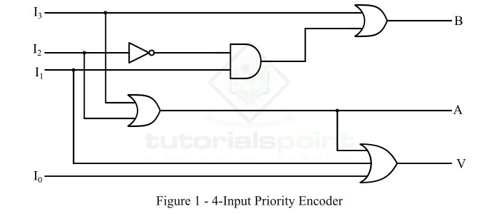
It has three outputs designated by A, B, and V. Where, A and B are the ordinary outputs and V is the output that acts as a valid bit indicator. This third output V is set to 1 when one or more inputs are equal to 1. In the case, when all the inputs to the encoder are equal to 0, there is no any valid input, and thus the output V is set to 0. The other two outputs, i.e. A and B of the encoder are not determined when V is equal to 0. Therefore, when, V is equal to 0, the outputs A and B are specified as "dont care conditions".
The truth table of the 4-input priority encoder is shown below.
| Inputs (X = Dont care) | Outputs | |||||
|---|---|---|---|---|---|---|
| I0 | I1 | I2 | I3 | A | B | V |
| 0 | 0 | 0 | 0 | X | X | 0 |
| 1 | 0 | 0 | 0 | 0 | 0 | 1 |
| X | 1 | 0 | 0 | 0 | 1 | 1 |
| X | X | 1 | 0 | 1 | 0 | 1 |
| X | X | X | 1 | 1 | 1 | 1 |
From this truth table, it can be observed that the higher the subscript number of the input, the higher the priority of the input. Thus, the input I3 has the highest priority. Therefore, regardless of the values of other inputs, when the input I3 is equal to 1, the output for AB is 11, i.e. 3. The input I2 has the next lower priority, and then I1, and finally I0 has the lowest priority.
We can write the Boolean expression for outputs A, B, and V from the above table as follows,
$$\mathrm{A \: = \: I_{3} \: + \: \bar{I_{3}} \: I_{2}\: = \: I_{3} \: + \: I_{2}}$$
$$\mathrm{B \: = \: I_{3} \: + \: \bar{I_{3}} \: \bar{I_{2}} \: I_{1} \: = \: I_{3} \: + \: \bar{I_{2}} \: I_{1}}$$
And,
$$\mathrm{V \: = \: I_{3} \: + \: I_{2} \: + \: I_{1} \: + \: I_{0}}$$
Hence, the condition for the output V is an OR operation of all the input variables.
Decimal to BCD Priority Encoder
This type of priority encoder performs the function of encoding the decimal digits into 4-bit BCD (Binary Coded Decimal) outputs. As it is a decimal to BCD priority encoder, therefore, it produces a BCD corresponding to the decimal digit of highest priority among all the inputs and ignores all others.
The truth table of the decimal to BCD priority encoder is given below.
| Decimal Inputs (X = Dont care) | BCD Outputs | |||||||||||
|---|---|---|---|---|---|---|---|---|---|---|---|---|
| I1 | I2 | I3 | I4 | I5 | I6 | I7 | I8 | I9 | A3 | A2 | A1 | A0 |
| 1 | 1 | 1 | 1 | 1 | 1 | 1 | 1 | 1 | 1 | 1 | 1 | 1 |
| X | X | X | X | X | X | X | X | 0 | 0 | 1 | 1 | 0 |
| X | X | X | X | X | X | X | 0 | 1 | 0 | 1 | 1 | 1 |
| X | X | X | X | X | X | 0 | 1 | 1 | 1 | 0 | 0 | 0 |
| X | X | X | X | X | 0 | 1 | 1 | 1 | 1 | 0 | 0 | 1 |
| X | X | X | X | 0 | 1 | 1 | 1 | 1 | 1 | 0 | 1 | 0 |
| X | X | X | 0 | 1 | 1 | 1 | 1 | 1 | 1 | 0 | 1 | 1 |
| X | X | 0 | 1 | 1 | 1 | 1 | 1 | 1 | 1 | 1 | 0 | 0 |
| X | 0 | 1 | 1 | 1 | 1 | 1 | 1 | 1 | 1 | 1 | 0 | 1 |
| 0 | 1 | 1 | 1 | 1 | 1 | 1 | 1 | 1 | 1 | 1 | 1 | 0 |
The truth table of the decimal to BCD priority encoder clearly shows that the magnitudes of the decimal inputs determine their priorities. If any decimal input is HIGH, it will be encoded if all other higher value inputs are LOW regardless of the state of all lower value inputs.
Octal to Binary Priority Encoder
This type of priority encoder is used to perform encoding of octal code into binary code. Hence, this type priority encoder has eight inputs and three outputs that produce corresponding binary code as given in the truth table below.
| Inputs | Outputs | ||||||||||
|---|---|---|---|---|---|---|---|---|---|---|---|
| I0 | I1 | I2 | I3 | I4 | I5 | I6 | I7 | A2 | A1 | A0 | V |
| 0 | 0 | 0 | 0 | 0 | 0 | 0 | 0 | X | X | X | 0 |
| 1 | 0 | 0 | 0 | 0 | 0 | 0 | 0 | 0 | 0 | 0 | 1 |
| X | 1 | 0 | 0 | 0 | 0 | 0 | 0 | 0 | 0 | 1 | 1 |
| X | X | 1 | 0 | 0 | 0 | 0 | 0 | 0 | 1 | 0 | 1 |
| X | X | X | 1 | 0 | 0 | 0 | 0 | 0 | 1 | 1 | 1 |
| X | X | X | X | 1 | 0 | 0 | 0 | 1 | 0 | 0 | 1 |
| X | X | X | X | X | 1 | 0 | 0 | 1 | 0 | 1 | 1 |
| X | X | X | X | X | X | 1 | 0 | 1 | 1 | 0 | 1 |
| X | X | X | X | X | X | X | 1 | 1 | 1 | 1 | 1 |
This is all about the priority encoder and its major types in digital electronics.
Digital Electronics - Decoders
What is a Decoder?
In digital electronics, a combinational logic circuit that converts an N-bit binary input code into M output channels in such a way that only one output channel is activated for each one of the possible combinations of inputs is known as a decoder.
In other words, a combinational logic circuit which converts N input lines into a maximum of 2N output lines is called a decoder.
Therefore, a decoder is a combination logic circuit that is capable of identifying or detecting a particular code. The operation that a decoder performs is referred to as decoding. A general block diagram of a decoder is shown in Figure-1.
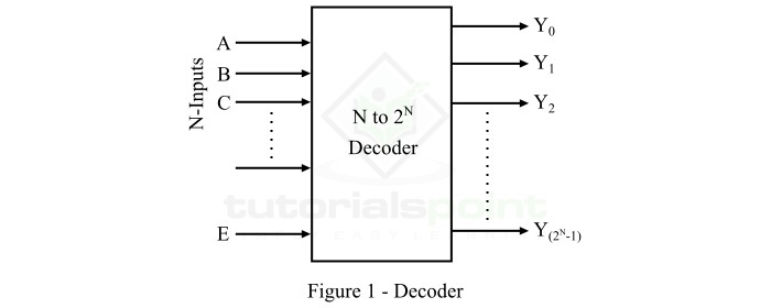
Here, the decoder has N input lines and M (2N) output lines. In a decoder, each of the N input lines can be a 0 or a 1, hence the number of possible input combinations or codes be equal to 2N. For each of these input combinations, only one of the M output lines will be active, and all other output lines will remain inactive.
Types of Decoders
There are several types of decoder present. But, based on the input and output lines present, decoders may classified into the following three types −
- 2 to 4 Decoder
- 3 to 8 Decoder
- 4 to 16 Decoder
Now, let us discuss each type of decoder in detail one by one.
2 to 4 Decoder
The 2 to 4 decoder is one that has 2 input lines and 4 (22) output lines. The functional block diagram of the 2 to 4 decoder is shown in Figure-2.
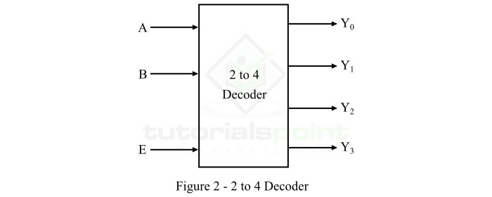
When this decoder is enabled with the help of enable input E, then its one of the four outputs will be active for each combination of inputs. The operation of this 2-line to 4-line decoder can be analyzed with the help of its truth table which is given below.
| Inputs | Outputs | |||||
|---|---|---|---|---|---|---|
| E | A | B | Y3 | Y2 | Y1 | Y0 |
| 0 | X | X | 0 | 0 | 0 | 0 |
| 1 | 0 | 0 | 0 | 0 | 0 | 1 |
| 1 | 0 | 1 | 0 | 0 | 1 | 0 |
| 1 | 1 | 0 | 0 | 1 | 0 | 0 |
| 1 | 1 | 1 | 1 | 0 | 0 | 0 |
Using this truth table, we can derive the Boolean expression for each output as follows −
$$\mathrm{Y_{0} \: = \: E \: \cdot \: \bar{A} \: \cdot \: \bar{B}}$$
$$\mathrm{Y_{1} \: = \: E \: \cdot \: \bar{A} \: \cdot \: B}$$
$$\mathrm{Y_{2} \: = \: E \: \cdot \: A \: \cdot \: \bar{B}}$$
$$\mathrm{Y_{3} \: = \: E \: \cdot \: A \: \cdot \: B}$$
As each output term contains products of input variables that can be implemented with the help of AND gates. Therefore, the logic circuit diagram of the 2 to 4 decoder is shown in Figure-3.

Operation
The operation of logic circuit of the 2 to 4 decoder is described as follows −
- When enable input (E) is inactive, i.e. set to 0, none of the AND gates will function.
- When enable input (E) is made active by setting it to 1, then the circuit works as explained below.
- When A = 0 and B = 0, the AND gate 1 becomes active and produces output Y0.
- When A = 0 and B = 1, the AND gate 2 becomes active and produces output Y1.
- When A = 1 and B = 0, the AND gate 3 becomes active and produces output Y2.
- When A = 1 and B = 1, the AND gate 4 becomes active and produces output Y3.
3 to 8 Decoder
The 3 to 8 decoder is one that has 3 input lines and 8 (23) output lines. The functional block diagram of the 3 to 8 decoder is shown in Figure-4.

When this decoder is enabled with the help of enable input E, then it's one of the eight outputs will be active for each combination of inputs. The operation of this 3-line to 8-line decoder can be analyzed with the help of its function table which is given below.
| Inputs | Outputs | ||||||||||
|---|---|---|---|---|---|---|---|---|---|---|---|
| E | A | B | C | Y7 | Y6 | Y5 | Y4 | Y3 | Y2 | Y1 | Y0 |
| 0 | X | X | X | 0 | 0 | 0 | 0 | 0 | 0 | 0 | 0 |
| 1 | 0 | 0 | 0 | 0 | 0 | 0 | 0 | 0 | 0 | 0 | 1 |
| 1 | 0 | 0 | 1 | 0 | 0 | 0 | 0 | 0 | 0 | 1 | 0 |
| 1 | 0 | 1 | 0 | 0 | 0 | 0 | 0 | 0 | 1 | 0 | 0 |
| 1 | 0 | 1 | 1 | 0 | 0 | 0 | 0 | 1 | 0 | 0 | 0 |
| 1 | 1 | 0 | 0 | 0 | 0 | 0 | 1 | 0 | 0 | 0 | 0 |
| 1 | 1 | 0 | 1 | 0 | 0 | 1 | 0 | 0 | 0 | 0 | 0 |
| 1 | 1 | 1 | 0 | 0 | 1 | 0 | 0 | 0 | 0 | 0 | 0 |
| 1 | 1 | 1 | 1 | 1 | 0 | 0 | 0 | 0 | 0 | 0 | 0 |
Using this function table, we can derive the Boolean expression for each output as follows −
$$\mathrm{Y_{0} \: = \: E \: \bar{A} \: \bar{B} \: \bar{C}}$$
$$\mathrm{Y_{1} \: = \: E \: \bar{A} \: \bar{B} \: C}$$
$$\mathrm{Y_{2} \: = \: E \: \bar{A} \: B \: \bar{C}}$$
$$\mathrm{Y_{3} \: = \: E \: \bar{A} \: B \: C}$$
$$\mathrm{Y_{4} \: = \: E \: A \: \bar{B} \: \bar{C}}$$
$$\mathrm{Y_{5} \: = \: E \: A \: \bar{B} \: C}$$
$$\mathrm{Y_{6} \: = \: E \: A \: B \: \bar{C}}$$
$$\mathrm{Y_{7} \: = \: E \: A \: B \: C}$$
As we can see, each output term contains products of input variables, hence they can be implemented with the help of AND gates. Therefore, the logic circuit diagram of the 3 to 8 decoder is shown in Figure-5.
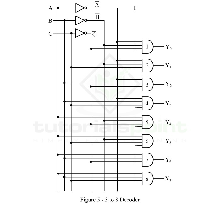
Operation
The operation of logic circuit of the 3 to 8 decoder is described as follows −
- When enable input (E) is inactive, i.e. set to 0, none of the AND gates will function.
- When enable input (E) is made active by setting it to 1, then the circuit works as described below.
- When A = 0, B = 0, and C = 0, the AND gate 1 becomes active and produces output Y0.
- When A = 0, B = 0, and C = 1, the AND gate 2 becomes active and produces output Y1.
- When A = 0, B = 1, and C = 0, the AND gate 3 becomes active and produces output Y2.
- When A = 0, B = 1, and C = 1, the AND gate 4 becomes active and produces output Y3.
- When A = 1, B = 0, and C = 0, the AND gate 5 becomes active and produces output Y4.
- When A = 1, B = 0, and C = 1, the AND gate 6 becomes active and produces output Y5.
- When A = 1, B = 1, and C = 0, the AND gate 7 becomes active and produces output Y6.
- When A = 1, B = 1, and C = 1, the AND gate 8 becomes active and produces output Y7.
4 to 16 Decoder
The 4 to 16 decoder is the type of decoder which has 4 input lines and 16 (214) output lines. The functional block diagram of the 4 to 16 decoder is shown in Figure-6.

When this decoder is enabled with the help of enable input E, it's one of the sixteen outputs will be active for each combination of inputs. The operation of the 4-line to 16-line decoder can be analyzed with the help of its function table which is given below.
| Inputs | Output | ||||
|---|---|---|---|---|---|
| E | A | B | C | D | |
| 0 | X | X | X | X | 0 |
| 1 | 0 | 0 | 0 | 0 | Y0 |
| 1 | 0 | 0 | 0 | 1 | Y1 |
| 1 | 0 | 0 | 1 | 0 | Y2 |
| 1 | 0 | 0 | 1 | 1 | Y3 |
| 1 | 0 | 1 | 0 | 0 | Y4 |
| 1 | 0 | 1 | 0 | 1 | Y5 |
| 1 | 0 | 1 | 1 | 0 | Y6 |
| 1 | 0 | 1 | 1 | 1 | Y7 |
| 1 | 1 | 0 | 0 | 0 | Y8 |
| 1 | 1 | 0 | 0 | 1 | Y9 |
| 1 | 1 | 0 | 1 | 0 | Y10 |
| 1 | 1 | 0 | 1 | 1 | Y11 |
| 1 | 1 | 1 | 0 | 0 | Y12 |
| 1 | 1 | 1 | 0 | 1 | Y13 |
| 1 | 1 | 1 | 1 | 0 | Y14 |
| 1 | 1 | 1 | 1 | 1 | Y15 |
From this function table, we can directly write the Boolean expression for each output as follows −
$$\mathrm{Y_{0} \: = \: E \: \bar{A} \: \bar{B} \: \bar{C} \: \bar{D}}$$
$$\mathrm{Y_{1} \: = \: E \: \bar{A} \: \bar{B} \: \bar{C} \: D}$$
$$\mathrm{Y_{2} \: = \: E \: \bar{A} \: \bar{B} \: C \: \bar{D}}$$
$$\mathrm{Y_{3} \: = \: E \: \bar{A} \: \bar{B} \: C \: D}$$
$$\mathrm{Y_{4} \: = \: E \: \bar{A} \: B \: \bar{C} \: \bar{D}}$$
$$\mathrm{Y_{5} \: = \: E \: \bar{A} \: B \: \bar{C} \: D}$$
$$\mathrm{Y_{6} \: = \: E \: \bar{A} \: B \: C \: \bar{D}}$$
$$\mathrm{Y_{7} \: = \: E \: \bar{A} \: B \: C \: D}$$
$$\mathrm{Y_{8} \: = \: E \: A \: \bar{B} \: \bar{C} \: \bar{D}}$$
$$\mathrm{Y_{9} \: = \: E \: A \: \bar{B} \: \bar{C} \: D}$$
$$\mathrm{Y_{10} \: = \: E \: A \: \bar{B} \: C \: \bar{D}}$$
$$\mathrm{Y_{11} \: = \: E \: A \: \bar{B} \: C \: D}$$
$$\mathrm{Y_{12} \: = \: E \: A \: B \: \bar{C} \: \bar{D}}$$
$$\mathrm{Y_{13} \: = \: E \: A \: B \: \bar{C} \: D}$$
$$\mathrm{Y_{14} \: = \: E \: A \: B \: C \: \bar{D}}$$
$$\mathrm{Y_{15} \: = \: E \: A \: B \: C \: D}$$
We can implement these output expression in the same way as we done for the 2 to 4 decoder and 3 to 8 decoder.
Now, let us discuss the applications of decoders.
Applications of Decoders
Decoders are used in the cases where an output or a collection of outputs is to be activated only on the occurrence of a particular combination of input codes. Some important applications of decoders are listed below −
- Decoders are used for code conversions.
- Decoders are extensively used in memory systems of computers.
- Decoders are also used for de-multiplexing or data distribution.
- Decoders are also used in data routing applications where very short propagation delay is required.
- Decoder may also be used for timing or sequencing purposes.
- Decoders are also utilized to turn on and off digital devices at a specific time.
This is all about decoder and its applications in digital electronic systems.
Digital Electronics - Demultiplexers
What is a Demultiplexer?
A Demultiplexer is a combinational logic circuit that accepts a single input and distributes it over several output lines. Demultiplexer is also termed as DEMUX in short. As Demultiplexer is used to transmit the same data to different destinations, hence it is also known as data distributor.
There is another combinational logic circuit named multiplexer which performs opposite operation of the Demultiplexer, i.e. accepts several inputs and transmits one of them at time to the output line.
From the definition, we can state that a Demultiplexer is a 1-to-2n device. The functional block diagram of a typical 1×2n Demultiplexer is shown in Figure-1.

It can be seen that the Demultiplexer has only one data input line, 2n output lines, and n select lines. The logic level applied to select lines of the Demultiplexer determines the output channel to which the input data will be transmitted.
Demultiplexer circuit are the combinational logic circuit widely used in digital decoders and Boolean function generator circuits.
Types of Demultiplexer
Based on the number of output lines (2n), Demultiplexers can be classified into several types. Some commonly used types of Demultiplexers are −
- 1×2 Demultiplexer
- 1×4 Demultiplexer
Now, let us briefly discuss each type of Demultiplexer.
1×2 Demultiplexer
The functional block diagram of a 1×2 Demultiplexer is shown in Figure-2.

The 1×2 Demultiplexer consists of 1 input line (I), 1 select line (S), and 2 output lines (Y0 and Y1). The logic level applied at the select line determines the output line to which the input data will be transmitted.
The operation of the 1×2 Demultiplexer can be analyzed with the help of its function table given below.
| Select Line | Outputs | |
|---|---|---|
| S | Y1 | Y0 |
| 0 | 0 | I |
| 1 | I | 0 |
From this function table of 1×2 Demultiplexer, we can directly derive the Boolean expression for each output as follow.
$$\mathrm{Y_{0} \: = \: \bar{S} \: I}$$
And,
$$\mathrm{Y_{1} \: = \: S \: I}$$
1×4 Demultiplexer
The functional block diagram of 1×4 Demultiplexer is shown in Figure-3.

The 1×4 Demultiplexer has 1 input line (I), 2 select line (S0 and S1), and 4 output lines (Y0, Y1, Y2, and Y3). The logic level applied to the select lines determines the output line to which the input data (I) will be transmitted.
The operation of the 1×4 Demultiplexer can be understood with the help of its function table given below.
| Select Line | Outputs | ||||
|---|---|---|---|---|---|
| S1 | S0 | Y3 | Y2 | Y1 | Y0 |
| 0 | 0 | 0 | 0 | 0 | I |
| 0 | 1 | 0 | 0 | I | 0 |
| 1 | 0 | 0 | I | 0 | 0 |
| 1 | 1 | I | 0 | 0 | 0 |
From this truth table of 1×4 Demultiplexer, we can directly write the Boolean expression for each output as follow.
$$\mathrm{Y_{0} \: = \: \bar{S_{1}} \: \bar{S_{0}} \: I}$$
$$\mathrm{Y_{1} \: = \: \bar{S_{1}} \: S_{0} \: I}$$
$$\mathrm{Y_{2} \: = \: S_{1} \: \bar{S_{0}} \: I}$$
$$\mathrm{Y_{3} \: = \: S_{1} \: S_{0} \: I}$$
We can easily understand the operation of the above circuit. Similarly, you can implement 1×8 Demultiplexer and 1×16 Demultiplexer by following the same procedure.
Implementation of Higher-order Demultiplexer
Now, let us implement the following two higher-order Demultiplexers using lower-order Demultiplexers.
- 1×8 Demultiplexer
- 1×16 Demultiplexer
1×8 Deultiplexer
In this section, let us implement 1×8 Demultiplexer using 1×4 Demultiplexers and 1×2 Demultiplexer. We know that 1×4 Demultiplexer has single input, two selection lines and four outputs. Whereas, 1×8 Demultiplexer has single input, three selection lines and eight outputs.
So, we require two 1×4 Demultiplexers in second stage in order to get the final eight outputs. Since, the number of inputs in second stage is two, we require 1×2 Demultiplexer in first stage so that the outputs of first stage will be the inputs of second stage. Input of this 1×2 Demultiplexer will be the overall input of 1×8 Demultiplexer.
Let the 1×8 Demultiplexer has one input I, three selection lines s2, s1 & s0 and outputs Y7 to Y0. The Truth table of 1×8 Demultiplexer is shown below.
| Selection Inputs | Outputs | |||||||||
|---|---|---|---|---|---|---|---|---|---|---|
| s2 | s1 | s0 | Y7 | Y6 | Y5 | Y4 | Y3 | Y2 | Y1 | Y0 |
| 0 | 0 | 0 | 0 | 0 | 0 | 0 | 0 | 0 | 0 | I |
| 0 | 0 | 1 | 0 | 0 | 0 | 0 | 0 | 0 | I | 0 |
| 0 | 1 | 0 | 0 | 0 | 0 | 0 | 0 | I | 0 | 0 |
| 0 | 1 | 1 | 0 | 0 | 0 | 0 | I | 0 | 0 | 0 |
| 1 | 0 | 0 | 0 | 0 | 0 | I | 0 | 0 | 0 | 0 |
| 1 | 0 | 1 | 0 | 0 | I | 0 | 0 | 0 | 0 | 0 |
| 1 | 1 | 0 | 0 | I | 0 | 0 | 0 | 0 | 0 | 0 |
| 1 | 1 | 1 | I | 0 | 0 | 0 | 0 | 0 | 0 | 0 |
We can implement 1×8 Demultiplexer using lower order Multiplexers easily by considering the above Truth table. The block diagram of 1×8 Demultiplexer is shown in the following figure.
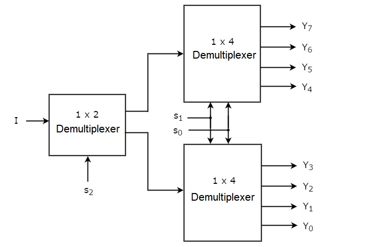
The common selection lines, s1 & s0 are applied to both 1×4 Demultiplexers. The outputs of upper 1×4 Demultiplexer are Y7 to Y4 and the outputs of lower 1×4 Demultiplexer are Y3 to Y0.
The other selection line, s2 is applied to 1×2 Demultiplexer. If s2 is zero, then one of the four outputs of lower 1×4 Demultiplexer will be equal to input, I based on the values of selection lines s1 & s0. Similarly, if s2 is one, then one of the four outputs of upper 1×4 Demultiplexer will be equal to input, I based on the values of selection lines s1 & s0.
1×16 Demultiplexer
In this section, let us implement 1×16 Demultiplexer using 1×8 Demultiplexers and 1×2 Demultiplexer. We know that 1×8 Demultiplexer has single input, three selection lines and eight outputs. Whereas, 1×16 Demultiplexer has single input, four selection lines and sixteen outputs.
So, we require two 1×8 Demultiplexers in second stage in order to get the final sixteen outputs. Since, the number of inputs in second stage is two, we require 1×2 Demultiplexer in first stage so that the outputs of first stage will be the inputs of second stage. Input of this 1×2 Demultiplexer will be the overall input of 1×16 Demultiplexer.
Let the 1×16 Demultiplexer has one input I, four selection lines s3, s2, s1 & s0 and outputs Y15 to Y0. The block diagram of 1×16 Demultiplexer using lower order Multiplexers is shown in the following figure.
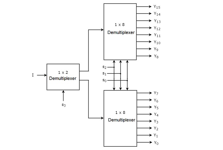
The common selection lines s2, s1 & s0 are applied to both 1×8 Demultiplexers. The outputs of upper 1×8 Demultiplexer are Y15 to Y8 and the outputs of lower 1×8 Demultiplexer are Y7 to Y0.
The other selection line, s3 is applied to 1×2 Demultiplexer. If s3 is zero, then one of the eight outputs of lower 1×8 Demultiplexer will be equal to input, I based on the values of selection lines s2, s1 & s0. Similarly, if s3 is one, then one of the 8 outputs of upper 1×8 Demultiplexer will be equal to input, I based on the values of selection lines s2, s1 & s0.
Integrated Circuits (ICs) Working as Demultiplexer
Demultiplexer can also be built in the form of ICs. There are several types of ICs available that work as Demultiplexer. Some common of them are listed below −
- 74139 IC works as a 1×4 Demultiplexer
- 74237 IC works as a 1×8 Demultiplexer
- 74154 IC works as a 1×16 Demultiplexer
Advantages of Demultiplexer
The important advantages of Demultiplexer are given below −
- By using Demultiplexers, we can increase the efficiency of the communication systems.
- Demultiplexer can separate different signals from a mixed signal stream.
- Demultiplexer can decode the signals produced by a multiplexer.
Disadvantages of Demultiplexer
The major disadvantages of Demultiplexers are listed below −
- The use of Demultiplexer can cause wastage of bandwidth.
- The synchronization of signals can create a delay in the system.
Applications of Demultiplexer
Demultiplexer is a crucial combinational logic circuit which is used in a number of applications. Some important uses of Demultiplexers are listed below −
- Demultiplexer are used in several input and output devices for data routing.
- Demultiplexer are used in digital control systems to select one signal from a mutual stream of signals.
- Demultiplexer are also employed for data transmission in synchronous systems.
- Demultiplexer are also utilized in data acquisition systems.
- Demultiplexer can be used for generating Boolean functions.
- Demultiplexer can be used in serial to parallel converters.
- Demultiplexer are used for broadcasting of ATM packets.
- Demultiplexer can also be used to design automatic test equipment, etc.
This is all about Demultiplexer, its types, and applications.
Arithmetic Logic Unit in Digital Electronics
The Arithmetic Logic Unit (ALU) is the fundamental component in a computing system like a computer. It is basically the actual data processing element within the central processing unit (CPU) in a computing system. It performs all the arithmetic and logical operations and forms the backbone of modern computer technology.
In this chapter, we will explain the working of the arithmetic logic unit, along with its main components, their functions, and the importance of the ALU in the field of digital system designs.
What is Arithmetic Logic Unit?
Arithmetic Logic Unit abbreviated as ALU is considered as the engine or heart of every central processing unit (CPU). ALU is basically a combination logic circuit that can perform arithmetic and logical operation on digital data (data in binary format). It can also execute instructions given to a computing system like a digital computer.

Within the complex architecture of a digital computing system, the arithmetic logic unit or ALU plays an important role as it executes and processes all the instructions, performs calculations, manipulates binary data, and performs various decision-making operations.
The development of arithmetic logic unit begins with the need for efficient, high speed, and accurate data processing and computation. With the advancement in electronics technologies, ALU has become a highly sophisticated digital data processing device that can handle a large number of complex instructions and computational tasks.
Todays ALU provides high accuracy, precision, and significantly fast processing speed in computing operations.
Features of Arithmetic Logic Unit
Here are some key features of arithmetic logic unit −
- The ALU can perform all arithmetic and logic operations such as addition, subtraction, multiplication, division, logical comparisons, etc.
- It can also perform bitwise and mathematical operations on binary numbers.
- It contains two segments namely, AU (arithmetic unit) and LU (logic unit) to perform arithmetic operations and logical operations respectively.
- It is the computational powerhouse within a central processing unit (CPU).
- ALU is the part of every CPU where actual data processing takes place.
- ALU is responsible for interpreting the code instructions based on which operations to be performed on the input data.
- Once the data processing is completed, the ALU sends the outcomes to the memory unit or output unit.
Main Components of Arithmetic Logic Unit
The arithmetic logic unit consists of various functional parts that are responsible for performing specific operations like addition, subtraction, multiplication, division, comparison, and more. Some of the key components of the arithmetic logic unit are explained below −
Arithmetic Unit
The main components used in the arithmetic unit (AU) segment of the arithmetic logic unit are as follows −
Adder
The adder or binary adder is one of the important components of the arithmetic logic unit. It performs the addition of two or more binary numbers. To accomplish this operation, it performs a series of logical and arithmetic operations. Some common types of adders used in the arithmetic ogic unit are half-adder, full-adder, parallel adder, and ripple carry adder. Each type of adder is designed and optimized to perform a specific computing operation.
Subtractor
The subtractor is another digital combinational circuit designed to perform subtraction of binary numbers. In most arithmetic logic unit, the subtractor uses 2s complement arithmetic to perform subtraction on binary numbers.
Multiplier and Divider
In more complex and advanced arithmetic logic units, dedicated multiplier and divider circuits are also implemented to perform multiplication and division on binary numbers. These circuits use advanced processing techniques like iterative or parallel processing to accomplish these operations.
Logic Unit
The logic unit (LU) of the ALU comprises the components responsible for performing Boolean or comparison operations. The following are some main components of the logic unit of an ALU −
Logic Gates
The logic gates like AND, OR, NOT, NAND, NOR, XOR, and XNOR are the key components of logic unit. These are standard logic circuits that can manipulate input data based on some predefined logical instructions and generate a desired output.
Each logic gate can perform a specific logical operation. However, different types of logic gates can be connected together in a specific manner to perform complex logical operations.
Type of Logic Gate
The brief overview of each type of logic gate is explained here −
- AND Gate − It performs the Boolean multiplication on input binary data. Its output is logic 1 or true, only when all its inputs are logic 1 or true.
- OR Gate − The OR gate performs the Boolean addition of input binary data. It generates a logic 1 or true output, if any of its inputs is logic 1 or true.
- NOR Gate − The NOT gate performs the inversion operation. It gives a logic 1 or true output when its input is logic 0 or false and vice-versa.
- NAND Gate − The NAND gate performs the NOTed AND operation and produces a logic 1 or true output when both inputs or any of the inputs is logic 0 or false.
- NOR Gate − The NOR gate performs the NOTed OR operation and generates a logic 1 or true output when all its inputs are logic 0 or false.
- XOR Gate − The XOR gate performs the exclusive OR operation and produces a logic 1 or true output when its both inputs are dissimilar. Hence, it is used as inequality detector.
- XNOR Gate − The XNOR gate performs the exclusive NOR operation and gives a logic 1 or true output when both its inputs are similar. Thus, it is used as an equality detector.
This is all about structure and components of the arithmetic logic unit. Let us now understand what functions an ALU can perform.
Functions of Arithmetic Logic Unit
The arithmetic logic unit can perform a wide range of functions and operations in digital computing systems. Some important functions that an arithmetic logic unit perform are explained below −
Arithmetic Operations
The arithmetic operations are one of the primary functions that the arithmetic logic unit performs. This category of operations includes addition, subtraction, multiplication, and division of binary numbers. All these operations form the basis of mathematical computations that the arithmetic logic unit can perform.
Logical Operations
The arithmetic logic unit can also perform various logical operations such as AND operation, OR operation, NOT operation, etc. These logical operations form the basis of decision making and data manipulation processes.
Comparison Operations
The arithmetic logic unit also facilitates to perform various comparison operations such as equal to, not equal to, less than, greater than, etc. These comparison operations are essential in decision making processes.
Shift Operations
The arithmetic logic unit can also perform shift operations on binary numbers such as left shift and right shift. These operations are important in multiplication and division operations. The shift operations can manipulate binary data at bit level and hence optimize the arithmetic calculations.
Working of Arithmetic Logic Unit
The working of the arithmetic logic unit depends on a combination of input data and control signals. In other words, the arithmetic logic unit receives the input data and control signals and then interpret these data and signals to perform specific operations.
Let us understand the working of the arithmetic logic unit in detail by breaking it down in sub-components.
Receiving Input Data and Control Signals
The arithmetic logic unit receives the input data from the user and a set of control signals that specifies the operation to be performed. The data is received through the input data path while the control signals are received from the control unit.
Execution of Operation
Once the arithmetic logic unit received the input data and control signals, it selects an appropriate functional component among arithmetic unit, logic unit, comparison unit, or shift unit to perform the specific operation. Once the operation completes, the ALU sends the results to the memory unit for storage or output unit.
Significance of Arithmetic Logic Unit
In the field of digital electronics and computing technology, the arithmetic logic unit plays an important role because of the following reasons −
- It can perform the arithmetic, logical, and comparison operations with very high accuracy, precision, and efficiency.
- It can also perform complex data processing and decision-making operations.
- ALU can execute complex processing tasks at a very high speed that results in better performance and higher efficiency.
- ALU introduces versatility as it can execute a wide range of computational tasks.
Conclusion
This is all about arithmetic logic unit (ALU) which is an important combinational logic circuit in digital electronics and modern computing systems. It acts as the heart of central processing unit (CPU) and executes all kinds of operations including arithmetic, logical, and comparison operations. In a digital computing system, the arithmetic logic unit acts as a primary functional unit that processes the input data based on the instructions. In this chapter, we have studied all the important concepts related to the arithmetic logic unit.
7-Segment LED Display
LED (Light Emitting Diode) is a semiconductor device that emits either visible light or infrared light when it is forward biased. Thus, it is widely used in different electronic devices like TV screens, mobile screens, watches and clocks, remote controls, etc. A light emitting diode (LED) basically converts electrical energy into light energy when an electric current flows through it.
In this article, we will discuss an application of LED in Seven Segment Display. The seven segment displays are extensively used in in different electronic gadgets like calculators, counters, watches, electronic measuring instruments, etc.
What is a Seven Segment LED Display?
Seven Segment Display is an LED based display screen that can display information in the form of decimal numbers. The seven segment display is a used in place of the more complex dot matrix displays. It is called so because it consists of seven segments of light emitting diodes (LEDs) that are assembled like decimal 8 as shown in the following figure.

Seven segments LED display can be used in applications where an electronic display device is required for showing decimal numbers from 0 to 9, sometimes, basic characters as well. Since, it uses LEDs, therefore it is an energy efficient display device. Therefore, it is most widely used in those devices that are powered by a small battery or a cell.
Working of Seven Segment LED Display
A seven segment display consists of seven LED segments arranged like a decimal 8. These LED segments are illuminated to form a pattern that represents a decimal number from 0 to 9. Now, let us understand, how the seven segment LED display work to display different numbers.
- When electrical energy is supplied to all the segments, then the seven segment LED display shows the decimal number 8.
- When power is given to all the segments and if we disconnect power from the segment g, then it displays the decimal number 0.
- When the power is given to segments "b" and "c" only, then it displays the number 1.
- When the power is given to the segments "a", "b", "g", "e", "d", then it displays the number 2.
- When the power is given to segments "a", "b", "g", "c", "d", then it displays the number 3.
- When the power is given to segments "b", "c", "f", "g", then it displays the number 4.
- When the power is given to segments "a", "c", "d", "f", "g", then it displays the number 5.
- When the power is given to segments "a", "c", "d", "e", "f", "g", then it displays the number 6.
- When the power is given to segments "a", "b", "c", then it displays the number 7.
- When the power is given to segments "a", "b", "c", "d", "f", "g", then it displays the number 9.
In this way, we can display any decimal number from 0 to 9 by illuminating a set of LED segments of the seven segment LED display.
Truth Table of Seven Segment LED Display
The following table shows the truth table of a seven segment LED display to display the decimal numbers from 0 to 9.
| Seven Segment Display Output | LED Segments Inputs | ||||||
|---|---|---|---|---|---|---|---|
| a | b | c | d | e | f | g | |
| 0 | 1 | 1 | 1 | 1 | 1 | 1 | 0 |
| 1 | 0 | 1 | 1 | 0 | 0 | 0 | 0 |
| 2 | 1 | 1 | 0 | 1 | 1 | 0 | 1 |
| 3 | 1 | 1 | 1 | 1 | 0 | 0 | 1 |
| 4 | 0 | 1 | 1 | 0 | 0 | 1 | 1 |
| 5 | 1 | 0 | 1 | 1 | 0 | 1 | 1 |
| 6 | 1 | 0 | 1 | 1 | 1 | 1 | 1 |
| 7 | 1 | 1 | 1 | 0 | 0 | 0 | 0 |
| 8 | 1 | 1 | 1 | 1 | 1 | 1 | 1 |
| 9 | 1 | 1 | 1 | 1 | 0 | 1 | 1 |
Types of Seven Segment LED Displays
There are two types of seven segment displays available −
Common Cathode Seven Segment Display
In this type of seven segment display, the cathode terminal of all LED segments are connected together to logic 0 (lower voltage level). The logic 1 (higher voltage level) is applied through a current limiting resistor to forward bias the individual LED segments at their anode terminals.
Common Anode Seven Segment Display
In this type of seven segment LED display, the anode terminals of all the LED segments are connected together to the logic 1 (higher voltage level), and the logic 0 (lower voltage level) is used through a current limiting resistor to the individual cathode terminals of LED segments.
Note − Common Anode Seven Segment LED Displays are more popular than Common Cathode Seven Segment Display because logic circuit can sink higher current as compared to they can source.
Applications of Seven Segment LED Displays
Seven Segment LED Displays are widely used in the following devices −
- Digital watches and clocks
- Calculators
- Microwaves
- Remote controls
- Speedometers
- Vehicle odometers
- Clock radios, etc.
Conclusion
Seven segment displays are very commonly used in low power electronic devices like remote controls, watches, clocks, digit measuring instruments, etc. From the above discussion, we may conclude that a seven segment display consists of seven LED (Light Emitting Diode) segments that are illuminated in a pattern to display the numbers from 0 to 9. Seven segment displays are also used to display some basic characters.
Digital Electronics - Code Converters
Code converters are important components in various digital systems and devices, as they help to connect different digital devices together that support data in different formats.
In this chapter, we will highlight different types of code converters used in digital electronics, their features, and applications.
What is a Code Converter?
A code converter is a digital electronic circuit that is used to convert a digital code from one form to another. A digital code is nothing but a piece of data or information represented in binary format, i.e., in the form of strings of 0s and 1s.
A code converter is simply a translator which translates a code from one format to another. For example, binary to decimal converter, BCD to Excess-3 converter, binary to decimal converter, etc.
Code converters are essential components in various digital systems that use different encoding schemes. They help to make two different digital systems compatible with each other.
For example, consider a digital system that supports data in binary format, and we need to connect this system with another system for processing that supports data in decimal format. Then, we need a data converter between them that can translate binary formatted data into decimal format for processing. This is how code converters play an important role in system interfacing.
Function of a Code Converter
The primary function of a code converter is to accept code in one format and translate it into a different format.
A code converter reads and interprets the input code and produces an equivalent output code according to its functionality. For example, a binary-to-decimal code converter takes a binary code as input and generates an equivalent decimal code as output.
Types of Code Converters
Depending on the conversion task that a code converter performs, the following are some common types of code converters −
- Binary to Decimal Converter
- Decimal to BCD Converter
- BCD to Decimal Converter
- Binary to Gray Code Converter
- Gray Code to Binary Converter
- BCD to Excess-3 Converter
- Excess-3 to BCD Converter
Let us discuss each of these types of code converters −
Binary to Decimal Converter
A type of code converter used to convert data from binary format to decimal format is called a binary-to-decimal converter.
The input to the binary-to-decimal converter is a number represented in a format of 0s and 1s. Then, the converter uses an algorithm to convert the input binary number into an equivalent decimal number. Finally, it generates a decimal code as output.
Decimal to BCD Converter
A decimal-to-BCD (Binary Coded Decimal) converter is a type of code convert that converts a decimal number into its equivalent 4-bit binary code, called BCD code.
BCD to Decimal Converter
A digital circuit that can convert a binary-coded decimal (BCD) number into an equivalent decimal number is referred to as a BCD-to-decimal converter.
The input to a BCD to decimal converter is an 8421 BCD code and the output generated by the converter is a decimal number.
Binary to Gray Code Converter
A binary-to-gray code converter is a type of code converter that can translate a binary code into its equivalent gray code.
The binary-to-gray code converter accepts a binary number as input and produces a corresponding gray code as output.
Gray Code to Binary Converter
A gray code-to-binary converter is a digital circuit that can translate a gray code into an equivalent pure binary code. Thus, a gray code to binary converter takes a gray code as input and gives a pure binary code as output.
BCD to Excess-3 Converter
A type of code converter in digital electronics that is used to convert a binary-coded decimal number into an equivalent excess-3 code is called a BCD to excess-3 converter.
Excess-3 to BCD Converter
An excess-3 to BCD converter is a type of code converter in digital electronics used to translate an XS-3 code into an equivalent binary-coded decimal.
Therefore, an XS-3 to BCD code converter accepts a digital code in XS-3 format and produces an equivalent digital code in BCD format.
Applications of Code Converters
In digital circuits and systems, the code converters are essential components that allow the conversion of a digital code from one format to another.
Some of the important applications of code converters are listed below −
- Code converters are used in ADC (Analog-to-Digital Converters) and DAC (Digital-to-Analog Converters).
- Code converters are used in computers to translate data between different digital formats.
- Code converters are also employed in display devices like seven segment displays, to convert binary codes into human readable form.
- In digital communication systems, the code converters are used to perform modulation and encoding tasks.
- The code converters are also used as interfacing device between two digital devices or systems that use different encoding schemes.
- Code converters are also used in digital signal processing applications to manipulate and process signals in different formats.
Code converters are integral parts of almost all digital systems and devices. They allow to interpret and process digital information in different formats.
Conclusion
A code converter is nothing but a digital circuit that can convert a digital code from one format like binary to another format like decimal.
Code converters are widely used in a variety of digital devices such as computers, smartphones, digital communication systems, microprocessors, microcontrollers, and more.
Binary to Decimal Converter
A type of code converter used to convert data from binary format to decimal format is called a binary-to-decimal converter.
The input to the binary-to-decimal converter is a number represented in a format of 0s and 1s. Then, the converter uses an algorithm to convert the input binary number into an equivalent decimal number. Finally, it generates a decimal code as output.
Let us now understand the logic circuit implementation of a binary-to-decimal converter.
The truth table of a two-bit binary-to-decimal converter is given below.
| Binary Input | Decimal Output | |
|---|---|---|
| B1 | B0 | |
| 0 | 0 | Q0 |
| 0 | 1 | Q1 |
| 1 | 0 | Q2 |
| 1 | 1 | Q3 |
Let us now derive the logical expression for each of the decimal outputs.
$$\mathrm{Q_{0} \: = \: \overline{B_{1}}\: \cdot \:\overline{B_{0}}}$$
$$\mathrm{Q_{1} \: = \: \overline{B_{1}}\: \cdot \: B_{0}}$$
$$\mathrm{Q_{2} \: = \: B_{1} \: \cdot \:\overline{B_{0}}}$$
$$\mathrm{Q_{3} \: = \: B_{1} \: \cdot \: B_{0}}$$
The logic circuit diagram of the binary-to-decimal converter is shown in the following figure.
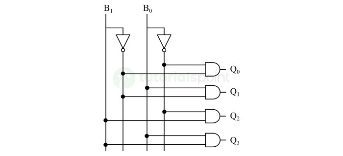
This circuit converts a 2-bit binary number into an equivalent decimal number. However, we can implement the binary-to-decimal converter for any number of bits in the same way.
Decimal to BCD Converter
A decimal-to-BCD (Binary Coded Decimal) converter is a type of code convert that converts a decimal number into its equivalent 4-bit binary code, called BCD code.
The truth table of the decimal to binary-coded decimal (BCD) converter is shown below.
| Decimal | BCD Code | |||
|---|---|---|---|---|
| B3 | B2 | B1 | B0 | |
| 0 | 0 | 0 | 0 | 0 |
| 1 | 0 | 0 | 0 | 1 |
| 2 | 0 | 0 | 1 | 0 |
| 3 | 0 | 0 | 1 | 1 |
| 4 | 0 | 1 | 0 | 0 |
| 5 | 0 | 1 | 0 | 1 |
| 6 | 0 | 1 | 1 | 0 |
| 7 | 0 | 1 | 1 | 1 |
| 8 | 1 | 0 | 0 | 0 |
| 9 | 1 | 0 | 0 | 1 |
The Boolean expressions for converting decimal to BCD are given below −
$$\mathrm{B_{0} \: = \: D_{1} \: + \: D_{3} \: + \: D_{5} \: + \: D_{7} \: + \: D_{9}}$$
$$\mathrm{B_{1} \: = \: D_{2} \: + \: D_{3} \: + \: D_{6} \: + \: D_{7}}$$
$$\mathrm{B_{2} \: = \: D_{4} \: + \: D_{5} \: + \: D_{6} \: + \: D_{7}}$$
$$\mathrm{B_{3} \: = \: D_{8} \: + \: D_{9}}$$
The logic circuit implementation of the decimal to BCD converter is shown in the following figure.
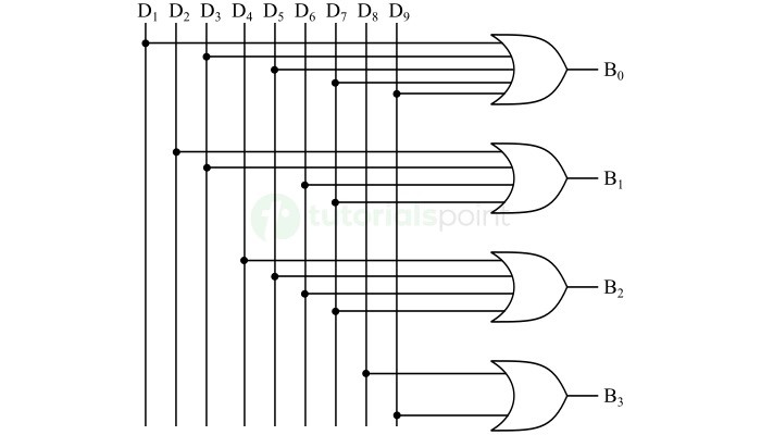
This logic circuit can perform the conversion of a given decimal number into a binary-coded decimal or BCD code.
BCD to Decimal Converter
A digital circuit that can convert a binary-coded decimal (BCD) number into an equivalent decimal number is referred to as a BCD-to-decimal converter.
The input to a BCD to decimal converter is an 8421 BCD code and the output generated by the converter is a decimal number.
The following is the truth table of the BCD to decimal converter describing its operation.
| BCD Code | Decimal | |||
|---|---|---|---|---|
| B3 | B2 | B1 | B0 | |
| 0 | 0 | 0 | 0 | D0 |
| 0 | 0 | 0 | 1 | D1 |
| 0 | 0 | 1 | 0 | D2 |
| 0 | 0 | 1 | 1 | D3 |
| 0 | 1 | 0 | 0 | D4 |
| 0 | 1 | 0 | 1 | D5 |
| 0 | 1 | 1 | 0 | D6 |
| 0 | 1 | 1 | 1 | D7 |
| 1 | 0 | 0 | 0 | D8 |
| 1 | 0 | 0 | 1 | D9 |
We can derive the Boolean expressions for each of the decimal outputs in terms of 8421 BCD code. These Boolean expressions are given below −
$$\mathrm{D_{0} \: = \: \overline{B_{3}} \: \overline{B_{2}} \: \overline{B_{1}} \: \overline{B_{0}}}$$
$$\mathrm{D_{1} \: = \: \overline{B_{3}} \: \overline{B_{2}} \: \overline{B_{1}} \: B_{0}}$$
$$\mathrm{D_{2} \: = \: \overline{B_{3}} \: \overline{B_{2}} \: B_{1} \: \overline{B_{0}}}$$
$$\mathrm{D_{3} \: = \: \overline{B_{3}} \: \overline{B_{2}} \: B_{1} \: B_{0}}$$
$$\mathrm{D_{4} \: = \: \overline{B_{3}} \: B_{2} \: \overline{B_{1}} \: \overline{B_{0}}}$$
$$\mathrm{D_{5} \: = \: \overline{B_{3}} \: B_{2} \: \overline{B_{1}} \: B_{0}}$$
$$\mathrm{D_{6} \: = \: \overline{B_{3}} \: B_{2} \: B_{1} \: \overline{B_{0}}}$$
$$\mathrm{D_{7} \: = \: \overline{B_{3}} \: B_{2} \: B_{1} \: B_{0}}$$
$$\mathrm{D_{8} \: = \: B_{3} \: \overline{B_{2}} \: \overline{B_{1}} \: \overline{B_{0}}}$$
$$\mathrm{D_{9} \: = \: B_{3} \: \overline{B_{2}} \: \overline{B_{1}} \: B_{0}}$$
The logic circuit implementation of the BCD to decimal converter is shown in the following figure.

Binary to Gray Code Converter
A binary-to-gray code converter is a type of code converter that can translate a binary code into its equivalent gray code.
The binary-to-gray code converter accepts a binary number as input and produces a corresponding gray code as output.
Here is the truth table explaining the operation of a 4-bit binary-to-gray code converter.
| Binary Code | Gray Code | ||||||
|---|---|---|---|---|---|---|---|
| B3 | B2 | B1 | B0 | G3 | G2 | G1 | G0 |
| 0 | 0 | 0 | 0 | 0 | 0 | 0 | 0 |
| 0 | 0 | 0 | 1 | 0 | 0 | 0 | 1 |
| 0 | 0 | 1 | 0 | 0 | 0 | 1 | 1 |
| 0 | 0 | 1 | 1 | 0 | 0 | 1 | 0 |
| 0 | 1 | 0 | 0 | 0 | 1 | 1 | 0 |
| 0 | 1 | 0 | 1 | 0 | 1 | 1 | 1 |
| 0 | 1 | 1 | 0 | 0 | 1 | 0 | 1 |
| 0 | 1 | 1 | 1 | 0 | 1 | 0 | 0 |
| 1 | 0 | 0 | 0 | 1 | 1 | 0 | 0 |
| 1 | 0 | 0 | 1 | 1 | 1 | 0 | 1 |
| 1 | 0 | 1 | 0 | 1 | 1 | 1 | 1 |
| 1 | 0 | 1 | 1 | 1 | 1 | 1 | 0 |
| 1 | 1 | 0 | 0 | 1 | 0 | 1 | 0 |
| 1 | 1 | 0 | 1 | 1 | 0 | 1 | 1 |
| 1 | 1 | 1 | 0 | 1 | 0 | 0 | 1 |
| 1 | 1 | 1 | 1 | 1 | 0 | 0 | 0 |
Let us derive the Boolean expressions for the gray code output bits. For this, we will simplify the truth table using the K-map technique.
K-Map for Gray Code Bit G0
The K-Map simplification to obtain the Boolean expression for the gray code bit G0 is shown in the following figure.
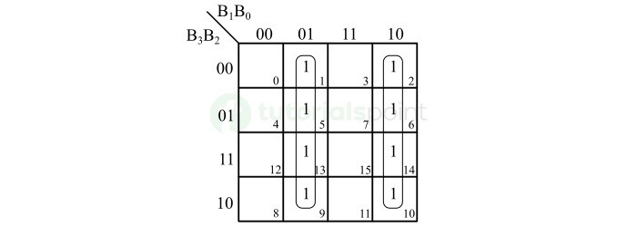
Hence, the Boolean expression for the gray code bit G0 is,
$$\mathrm{G_{0} \: = \: \overline{B_{1}} \: B_{0} \: + \ B_{1} \: \overline{B_{0}} \: = \: B_{0} \: \oplus \: B_{1}}$$
K-Map for Gray Code Bit G1
The K-Map simplification for the gray code bit G1 is shown below −

Thus, the Boolean expression for the gray code bit G1 is,
$$\mathrm{G_{1} \: = \: \overline{B_{2}} \: B_{1} \: + \ B_{2} \: \overline{B_{1}} \: = \: B_{1} \: \oplus \: B_{2}}$$
K-Map for Gray Code Bit G2
The K-Map simplification for the gray code bit G2 is depicted in the following figure −

The Boolean expression for the gray code bit G2 will be,
$$\mathrm{G_{2} \: = \: \overline{B_{3}} \: B_{2} \: + \ B_{3} \: \overline{B_{2}} \: = \: B_{2} \: \oplus \: B_{3}}$$
K-Map for Gray Code Bit G3
The K-Map simplification for the gray code bit G3 is shown in the following figure −

Hence, the Boolean expression for the gray code bit G3 is,
$$\mathrm{G_{3} \: = \: B_{3}}$$
Let us now utilize these Boolean expressions to implement the logic circuit of the binary-to-gray code converter.
The following figure shows the logic circuit diagram of a 4-bit binary code to gray code converter −
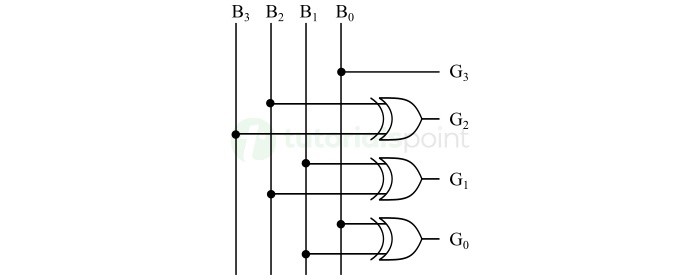
This circuit can convert a 4-bit binary number into an equivalent gray code.
We can follow the same procedure to design a binary-to-gray code converter for any number of bits.
Gray Code to Binary Converter
A gray code-to-binary converter is a digital circuit that can translate a gray code into an equivalent pure binary code. Thus, a gray code to binary converter takes a gray code as input and gives a pure binary code as output.
The truth table of a 3-bit gray code to binary code converter is given below −
| Gray Code | Binary Code | ||||
|---|---|---|---|---|---|
| G2 | G1 | G0 | B2 | B1 | B0 |
| 0 | 0 | 0 | 0 | 0 | 0 |
| 0 | 0 | 1 | 0 | 0 | 1 |
| 0 | 1 | 0 | 0 | 1 | 1 |
| 0 | 1 | 1 | 0 | 1 | 0 |
| 1 | 0 | 0 | 1 | 1 | 1 |
| 1 | 0 | 1 | 1 | 1 | 0 |
| 1 | 1 | 0 | 1 | 0 | 0 |
| 1 | 1 | 1 | 1 | 0 | 1 |
Let us obtain the Boolean expression for the binary output bits. For this, we will simplify the truth table using the K-map technique.
K-Map for Binary Bit B0
The K-map simplification for the binary output bit B0 is shown in the following figure.

The Boolean expression for the binary bit B0 will be,
$$\mathrm{B_{0} \: = \: \overline{G_{2}} \: \overline{G_{1}} \: G_{0} \: + \: \overline{G_{2}} \: G_{1} \: \overline{G_{0}} \: + \: G_{2} \: \overline{G_{1}} \: \overline{G_{0}}\: + \: G_{2} \: G_{1} \: G_{0}}$$
We can further simplify this expression as follows,
$$\mathrm{\Rightarrow \: B_{0} \: = \: \overline{G_{2}} \: (\overline{G_{1}} \: G_{0} \: + \: G_{1} \: \overline{G_{0}}) \: + \: G_{2} \: (\overline{G_{1}} \: \overline{G_{0}}\: + \: G_{1} \: G_{0})}$$
$$\mathrm{\Rightarrow \: B_{0} \: = \: \overline{G_{2}} \: ( G_{0} \: \oplus \: G_{1}) \: + \: G_{2} \: \overline{(G_{0} \: \oplus \: G_{1})}}$$
$$\mathrm{B_{0} \: = \: G_{0} \: \oplus \: G_{1} \: \oplus \: G_{2}}$$
This is the simplified expression for the binary bit B0.
K-Map for Binary Bit B1
The K-map simplification for the binary output B1 is shown below.

The Boolean expression for the binary bit B1 is,
$$\mathrm{B_{1} \: = \: G_{2} \: \overline{G_{1}} \: + \: \overline{G_{2}} \: G_{1} \: = \: G_{1} \: \oplus \: G_{2}}$$
K-Map for Binary Bit B2
The following figure shows the K-map simplification for the binary bit B2.

From this K-Map, we obtain the following Boolean expression −
$$\mathrm{B_{2} \: = \: G_{2}}$$
The logic circuit implementation of this 3-bit gray to binary code converter is shown in the following figure.

This logic circuit can translate a 3-bit gray code into an equivalent 3-bit binary code. We can also follow the same procedure to implement a gray code to binary code converter for any number of bits.
BCD to Excess-3 Converter
A type of code converter in digital electronics that is used to convert a binary-coded decimal number into an equivalent excess-3 code is called a BCD to excess-3 converter.
Hence, in the case of a BCD to excess-3 code converter, the input is an 8421 BCD code and the output is an XS-3 code.
The following is the truth table of a BCD to excess-3 code converter −
| BCD Code | Excess-3 Code | ||||||
|---|---|---|---|---|---|---|---|
| B3 | B2 | B1 | B0 | X3 | X2 | X1 | X0 |
| 0 | 0 | 0 | 0 | 0 | 0 | 1 | 1 |
| 0 | 0 | 0 | 1 | 0 | 1 | 0 | 0 |
| 0 | 0 | 1 | 0 | 0 | 1 | 0 | 1 |
| 0 | 0 | 1 | 1 | 0 | 1 | 1 | 0 |
| 0 | 1 | 0 | 0 | 0 | 1 | 1 | 1 |
| 0 | 1 | 0 | 1 | 1 | 0 | 0 | 0 |
| 0 | 1 | 1 | 0 | 1 | 0 | 0 | 1 |
| 0 | 1 | 1 | 1 | 1 | 0 | 1 | 0 |
| 1 | 0 | 0 | 0 | 1 | 0 | 1 | 1 |
| 1 | 0 | 0 | 1 | 1 | 1 | 0 | 0 |
| 1 | 0 | 1 | 0 | X | X | X | X |
| 1 | 0 | 1 | 1 | X | X | X | X |
| 1 | 1 | 0 | 0 | X | X | X | X |
| 1 | 1 | 0 | 1 | X | X | X | X |
| 1 | 1 | 1 | 0 | X | X | X | X |
| 1 | 1 | 1 | 1 | X | X | X | X |
Let us solve the truth table using the K-map to derive the Boolean expressions for the XS-3 output bits X0, X1, X2, and X3.
K-Map for XS-3 Bit X0
The K-map simplification for the XS-3 bit X0 is shown in the following figure −

On simplifying this K-map, we obtain the following Boolean expression,
$$\mathrm{X_{0} \: = \: \overline{B_{0}}}$$
K-Map for XS-3 Bit X1
The K-map simplification for the XS-3 bit X1 is depicted below −
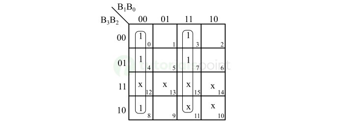
This K-map simplification gives the following Boolean expression,
$$\mathrm{X_{1} \: = \: \overline{B_{1}} \: \overline{B_{0}} \: + \: B_{1} \: B_{0}}$$
K-Map for XS-3 Bit X2
The K-map simplification for the XS-3 bit X2 is shown in the figure below.
On simplifying this K-map, we obtain the following Boolean expression,
$$\mathrm{X_{2} \: = \: \overline{B_{2}} \: B_{1} \: + \: \overline{B_{2}} \: B_{0} \: + \: B_{2} \: \overline{B_{1}} \: \overline{B_{0}}}$$
K-Map for XS-3 Bit X3
The K-map simplification for the XS-3 bit X3 is depicted in the figure below −

This K-map gives the following Boolean expression,
$$\mathrm{X_{3} \: = \: B_{3} \: + \: B_{2} \: B_{1} \: + \: B_{2} \: B_{0}}$$
The logic circuit diagram of the BCD to XS-3 converter is shown in the following figure −

This circuit converters a 4-bit BCD code into an equivalent XS-3 code.
Excess-3 to BCD Converter
An excess-3 to BCD converter is a type of code converter in digital electronics used to translate an XS-3 code into an equivalent binary-coded decimal.
Therefore, an XS-3 to BCD code converter accepts a digital code in XS-3 format and produces an equivalent digital code in BCD format.
The truth table of the XS-3 to BCD code converter is given below −
| Excess-3 Code | BCD Code | ||||||
|---|---|---|---|---|---|---|---|
| X3 | X2 | X1 | X0 | B3 | B2 | B1 | B0 |
| 0 | 0 | 0 | 0 | X | X | X | X |
| 0 | 0 | 0 | 1 | X | X | X | X |
| 0 | 0 | 1 | 0 | X | X | X | X |
| 0 | 0 | 1 | 1 | 0 | 0 | 0 | 0 |
| 0 | 1 | 0 | 0 | 0 | 0 | 0 | 1 |
| 0 | 1 | 0 | 1 | 0 | 0 | 1 | 0 |
| 0 | 1 | 1 | 0 | 0 | 0 | 1 | 1 |
| 0 | 1 | 1 | 1 | 0 | 1 | 0 | 0 |
| 1 | 0 | 0 | 0 | 0 | 1 | 0 | 1 |
| 1 | 0 | 0 | 1 | 0 | 1 | 1 | 0 |
| 1 | 0 | 1 | 0 | 0 | 1 | 1 | 1 |
| 1 | 0 | 1 | 1 | 1 | 0 | 0 | 0 |
| 1 | 1 | 0 | 0 | 1 | 0 | 0 | 1 |
| 1 | 1 | 0 | 1 | X | X | X | X |
| 1 | 1 | 1 | 0 | X | X | X | X |
| 1 | 1 | 1 | 1 | X | X | X | X |
Now, we will simplify this truth table using K-map method to obtain the Boolean expression for the output bits.
K-Map for BCD Bit B0
The following figure shows the K-map simplification for the BCD bit B0.

This K-map gives the following Boolean expression,
$$\mathrm{B_{0} \: = \: \overline{X_{0}}}$$
K-Map for BCD Bit B1
The following figure shows the K-map simplification for the BCD bit B1.
This K-map gives the following Boolean expression,
$$\mathrm{B_{1} \: = \: \overline{X_{1}} \: X_{0} \: + \: X_{1} \: X_{0}}$$
K-Map for BCD Bit B2
The K-map simplification for the BCD bit B2 is shown below −

The simplification of this K-map gives the following Boolean expression,
$$\mathrm{B_{2} \: = \: \overline{X_{2}} \: \overline{X_{1}} \: + \: \overline{X_{2}} \: \overline{X_{0}} \: + \: X_{2} \: X_{1} \: X_{0}}$$
K-Map for BCD Bit B3
The K-map simplification for the BCD bit B3 is shown in the following figure −
By simplifying this K-map, we obtain the following Boolean expression,
$$\mathrm{B_{3} \: = \: X_{3} \: X_{2} \: + \: X_{3} \: X_{1} \: X_{0}}$$
We can use these Boolean expressions to implement the digital logic circuit to perform the XS-3 to BCD conversion.
The logic circuit diagram to convert an XS-3 code into equivalent BCD code i.e., Excess-3 to BCD converter is shown in the following figure −

This is all about some commonly used digital code converters used in various digital electronic applications.
Half Adder in Digital Electronics
Addition is one of the most basic operations performed by different electronic devices like computers, calculators, etc. The electronic circuit that performs the addition of two or more numbers, more specifically binary numbers, is called as adder. Since, the logic circuits use binary number system to perform the operations, hence the adder is referred to as binary adder
Depending on the number of bits that the circuit can add, adders (or binary adders) are of two types −
- Half Adder
- Full Adder
In this article, we will discuss the half adder, its definition, circuit diagram, truth table, kmap, characteristic equations, and applications.
What is a Half-Adder?
A combinational logic circuit which is designed to add two binary digits is called as a half adder. The half adder provides the output along with a carry value (if any). The half adder circuit is designed by connecting an EX-OR gate and one AND gate. It has two input terminals and two output terminals for sum and carry. The block diagram and circuit diagram of a half adder are shown in Figure-1.

From the logic circuit diagram of half adder, it is clear that A and B are the two input bits, S is the output sum, and C is the output carry bit.
In the case of a half adder, the output of the EX-OR gate is the sum of two bits and the output of the AND gate is the carry. Although, the carry obtained in one addition will not be forwarded in the next addition because of this it is known as half adder.
Operation of Half Adder
Half adder adds two binary digits according to the rules of binary addition. These rules are as follows −
$$\mathrm{0 \: + \: 0 \: = \: 0}$$
$$\mathrm{0 \: + \: 1 \: = \: 1}$$
$$\mathrm{1 \: + \: 0 \: = \: 1}$$
$$\mathrm{1 \: + \: 1 \: = \: 10 \: (Sum \: = \: 0 \: \& \: Carry \: = \: 1)}$$
According to these rules of binary addition, we can see that the first three operations produce a sum whose length is one digit, whereas in the case of last operation (1 and 1), the sum consists of two digits. Here, the MSB (most significant bit) of this result is called a carry (which is 1) and the LSB (least significant bit) is called the sum (which is 0).
Truth Table of Half Adder
Truth table is one that gives the relationship between inputs and outputs of a logic circuit and explains the operation of the circuit. The following is the truth table of the half-adder −
| Inputs | Outputs | ||
|---|---|---|---|
| A | B | S (Sum) | C (Carry) |
| 0 | 0 | 0 | 0 |
| 0 | 1 | 1 | 0 |
| 1 | 0 | 1 | 0 |
| 1 | 1 | 0 | 1 |
K-Map for Half Adder
We can use the K-Map (Karnaugh Map), a method for simplifying Boolean algebra, to determine equations of the sum bit (S) and the output carry bit (C) of the half adder circuit.
The k-map for half adder circuit is shown in Figure-2.

Characteristic Equations of Half-Adder
The characteristic equations of half adder, i.e., equations of sum (S) and carry (C) are obtained according to the rules of binary addition. These equations are given below −
The sum (S) of the half-adder is the XOR of A and B. Thus,
$$\mathrm{Sum, \: S \: = \: A \: \oplus B \: = \: AB' \: + \: A'B }$$
The carry (C) of the half-adder is the AND of A and B. Therefore,
$$\mathrm{Carry, \: C \: = \: A \cdot B }$$
Applications of Half Adder
The following are some important applications of half adder −
- Half adder is used in ALU (Arithmetic Logic Unit) of computer processors to add binary bits.
- Half adder is used to realize full adder circuit.
- Half adder is used in calculators.
- Half adder is used to calculate addresses and tables.
Conclusion
From the above discussion, we can conclude that half adders are one of the basic arithmetic circuits used in different electronic devices to perform addition of two binary digits. The major drawback of a half adder is that it cannot add the carry obtained from the addition of the previous stage. To overcome this drawback, full adders are used in electronic systems.
Full Adder in Digital Electronics
What is a Full Adder?
A combinational logic circuit that can add two binary digits (bits) and a carry bit, and produces a sum bit and a carry bit as output is known as a full-adder.
In other words, a combinational circuit which is designed to add three binary digits and produces two outputs (sum and carry) is known as a full adder. Thus, a full adder circuit adds three binary digits, where two are the inputs and one is the carry forwarded from the previous addition. The block diagram and circuit diagram of the full adder are shown in Figure-1.

Hence, the circuit of the full adder consists of one EX-OR gate, three AND gates and one OR gate, which are connected together as shown in the full adder circuit in Figure-1.
Operation of Full Adder
Full adder takes three inputs namely A, B, and Cin. Where, A and B are the two binary digits, and Cin is the carry bit from the previous stage of binary addition. The sum output of the full adder is obtained by XORing the bits A, B, and Cin. While the carry output bit (Cout) is obtained using AND and OR operations.
Truth Table of Full Adder
Truth table is one that indicates the relationship between input and output variables of a logic circuit and explains the operation of the logic circuit. The following is the truth table of the full-adder circuit −
| Inputs | Outputs | |||
|---|---|---|---|---|
| A | B | Cin | S (Sum) | Cout (Carry) |
| 0 | 0 | 0 | 0 | 0 |
| 0 | 0 | 1 | 1 | 0 |
| 0 | 1 | 0 | 1 | 0 |
| 0 | 1 | 1 | 0 | 1 |
| 1 | 0 | 0 | 1 | 0 |
| 1 | 0 | 1 | 0 | 1 |
| 1 | 1 | 0 | 0 | 1 |
| 1 | 1 | 1 | 1 | 1 |
Hence, from the truth table, it is clear that the sum output of the full adder is equal to 1 when only 1 input is equal to 1 or when all the inputs are equal to 1. While the carry output has a carry of 1 if two or three inputs are equal to 1.
K-Map for Full Adder
K-Map (Karnaugh Map) is a tool for simplifying binary complex Boolean algebraic expressions. The K-Map for full adder is shown in Figure-2.

Characteristic Equations of Full Adder
The characteristic equations of the full adder, i.e. equations of sum (S) and carry output (Cout) are obtained according to the rules of binary addition. These equations are given below −
The sum (S) of the full-adder is the XOR of A, B, and Cin. Therefore,
$$\mathrm{Sum, \: S \: = \: A \: \oplus \: B \: \oplus \: C_{in} \: = \: A'B'C_{in} \: + \: A'BC'_{in} \: + \: AB'C'_{in} \: + \: ABC_{in} }$$
The carry (C) of the half-adder is the AND of A and B. Therefore,
$$\mathrm{Carry, \: C \: = \: AB \: + \: AC_{in} \: + \: BC_{in}}$$
Advantages of Full Adder
The following are the important advantages of full adder over half adder −
- Full adder provides facility to add the carry from the previous stage.
- The power consumed by the full adder is relatively less as compared to half adder.
- Full adder can be easily converted into a half subtractor just by adding a NOT gate in the circuit.
- Full adder produces higher output that half adder.
- Full adder is one of the essential part of critic digital circuits like multiplexers.
- Full adder performs operation at higher speed.
Applications of Full Adder
The following are the important applications of full adder −
- Full adders are used in ALUs (arithmetic logic units) of CPUs of computers.
- Full adders are used in calculators.
- Full adders also help in carrying out multiplication of binary numbers.
- Full adders are also used to realize critic digital circuits like multiplexers.
- Full adders are used to generate memory addresses.
- Full adders are also used in generation of program counterpoints.
- Full adders are also used in GPU (Graphical Processing Unit).
Conclusion
In this tutorial, we discussed all the key concepts related to full adders in digital electronics. Full adders play an important role in many digital electronic circuits because a full adder can be used realize several other critical digital circuits.
Digital Electronics - Serial Binary Adder
In digital electronics, the binary adder is a combinational logic circuit which performs the addition of two or more binary digits. The binary addition is performed based on the Boolean algebraic laws of addition, i.e.,
$$\mathrm{0 \: + \: 0 \: = \: 0}$$
$$\mathrm{0 \: + \: 1 \: = \: 1}$$
$$\mathrm{1 \: + \: 0 \: = \: 1}$$
$$\mathrm{1 \: + \: 1 \: = \: 0}$$
Binary adders are classified into two types namely, serial binary adder and parallel binary adder.
In this tutorial, we will discuss serial binary adder, its definition, logic circuit diagram, and operation. So, let us start with basic introduction of serial binary adder.
What is a Serial Binary Adder?
A serial binary adder is a binary adder circuit which is used to add binary numbers in serial form. In the serial adder, the two binary numbers which are added serially are stored in two shift registers, let shift register A and shift register B.
The logic circuit diagram of the serial binary adder is shown in Figure 1.
The function of different elements of the serial adder circuit is as follows −
Full Adder
Full adder is a digital combinational logic circuit which can add three binary digits and can produce two output bits, i.e. sum bit and carry bit. In the serial binary adder circuit, the full adder adds one pair of bits at a time.
Shift Register
A group of flip-flops that can store several bits of data is called a shift register. In serial binary adder, two shift registers are used, where one is for storing augend bit and the other is for storing added of the binary number.
D Flip-Flop
In serial adder, the D flip-flop is used to store the carry output bit. The output of this D flip-flop is used as the carry input in the next stage of addition.
Operation of Series Binary Adder
In the serial binary adder circuit, the binary digits (bits) are added one pair at a time using a full-adder circuit. The carry generated from the full adder is transferred to a D-flip flop. Thus, the output of this D-flip flop is then used as the carry input for the next pair of significant bits. The sum bit S is transferred to a third shift register. Now, let us understand the operation of the serial binary adder in the detail.
At beginning, the shift register A stores the augend bit of the given binary number, and the shift register B stores the addend bit. Initially, the D flip flop is cleared to 0, hence no carry bit is present. The outputs of shift registers A and B supply a pair of significant bits to the full adder circuit at inputs I0 and I1. A shift control is used to enable the shift registers A and B and the carry flip-flop.
Therefore, at each clock pulse, the registers A and B are shifted to the right, and the sum bit from output S of the full adder circuit enters the left most of the shift register A. Thus, for each succeeding clock pulse a new sum bit is transferred to the shift register A and a new carry bit is transferred to the output Q of the D flip flop. This process continues until the shift control is disabled.
Hence, the addition of two binary numbers in serial form is accomplished by supplying a pair of bits together with the previous carry to a full adder circuit, and transferring a sum bit at a time into the shift register A.
Now, we can summarize the working process of the serial binary adder as follows −
- Initially, the shift register A and the carry flip flop are set to 0, and the first number is added from the register B.
- When the register B is shifting through the full adder, a second number is transferred to it through its serial input.
- This second number is then added to the number of the register A, while a third number is transferred to into the register B through the serial input.
This process is executed repeatedly to perform the addition of two, three, or more binary number in serial form and accumulate the sum result in the shift register A.
Digital Electronics - N-bit Parallel Adders
Let us stat this article with a brief introduction of binary adders and rules of binary addition. In digital electronics, an adder or binary adder is a combinational digital circuit which performs the addition of two or more binary digits. The binary addition of two bits is performed by following these four rules −
$$\mathrm{0 \: + \: 0 \: = \: 0}$$
$$\mathrm{0 \: + \: 1 \: = \: 1}$$
$$\mathrm{1 \: + \: 0 \: = \: 1}$$
$$\mathrm{1 \: + \: 1 \: = \: 10 (Sum \: = \: 0; Carry \: = \: 1)}$$
The first three operations produce a sum whose bit length is one binary digit. But, the sum of last combination, i.e. when augend and addend both are equal to 1, the binary sum consists of two binary digits namely, sum bit and carry bit. The most significant bit is the carry bit, while the least significant bit is the sum bit.
We also require the knowledge of full-adder circuit for better understanding of the implementation and operation of an N-bit parallel adder. The full-adder along with its block diagram and truth table is describe below.
What is Full Adder?
A combination digital circuit that adds two bits and a carry bit and produces a sum bit and a carry bit as output is referred to as a full adder (FA).
In other words, a binary adder circuit that can add three input bits and produces two output bits, i.e. sum bit and carry bit is called full adder. The block diagram of a full adder is shown in Figure-1.

Here, A and B are the input bits, Cin is the input carry bit from previous sum, S is the output sum bit, and Cout is the output carry bit.
The operation of the full adder circuit can be understood easily from its truth table which is given below.
| Input | Output | |||
|---|---|---|---|---|
| A | B | Cin | S | Cout |
| 0 | 0 | 0 | 0 | 0 |
| 0 | 0 | 1 | 1 | 0 |
| 0 | 1 | 0 | 1 | 0 |
| 0 | 1 | 1 | 0 | 1 |
| 1 | 0 | 0 | 1 | 0 |
| 1 | 0 | 1 | 0 | 1 |
| 1 | 1 | 0 | 0 | 1 |
| 1 | 1 | 1 | 1 | 1 |
Now, let us discuss the realization of an N-bit parallel adder using full adders.
N-Bit Parallel Adder
Parallel adder is a binary adder circuit implemented to add two binary number having N-bits (for example, to add 4-bit binary numbers, we use 4- bit parallel adder, and so on). As its name implies, the parallel adder is a digital combinational circuit that adds two binary numbers in parallel form and generates the arithmetic sum of those binary numbers in parallel form.
As we already mentioned above that a full adder can perform addition of only two one-bit binary numbers consisting of two input bits and one input carry bit, i.e. addition of three bits. But in actual practice, we have to add such binary numbers whose length is more than one bit. To add such binary numbers, we use parallel binary adder which is capable of adding the two binary numbers of any bit length such as 4-bit, 5-bit, etc.
We can implement an N-bit parallel adder with the help of full-adders connected in a chain fashion. The block diagram representation of an N-bit parallel adder using full adders is shown in Figure-2.
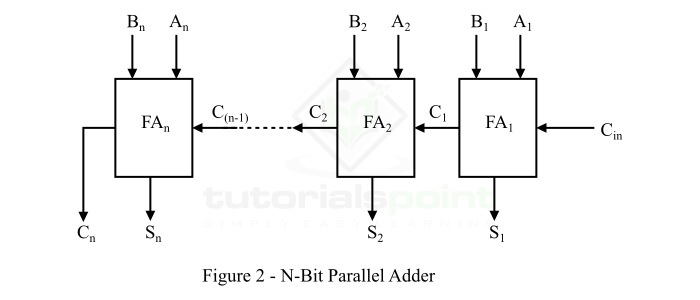
From the block diagram of the N-bit parallel adder, it can be seen that the carry output from each full-adder is connected to the carry input terminal of the next higher level full-adder in the chain.
The number of full-adder to realize a parallel adder is determined from the number of bits in the two binary numbers to be added. Therefore, an N-bit parallel adder requires N full-adders to perform the addition in parallel form. For example, a 2-bit parallel adder requires 2 full adders, 4-bit parallel adder consists of 4 full adders, and so on.
Operation of N-Bit Parallel Adder Circuit
The working of the N-bit parallel adder shown in figure-2 can be described in the following steps −
- Initially, the full adder FA1 adds two input bits A1 and B1 along with an input carry bit Cin, and it generates the output sum bit S1 and the carry bit C1 which is forwarded to the next adder (FA2) in the chain. The sum bit S1 is the least significant bit of the output sum.
- At the next stage, the full adder circuit FA2 becomes active and adds input bits A2 and B2 along with C1. It generates the sum bit S2 which is the second bit of the output sum, and the carry bit C2 that is connected to the next full adder FA3 in the chain.
- This process will continue till the last full adder, i.e. FAn in the chain. The full adder uses carry input C(n-1) to add with the input bits An and Bn to produce the last bit of the output sum Sn and the last output carry bit Cn.
Advantages of Parallel Adder
Some important advantages of parallel adder are listed below −
- The parallel adder adds bits simultaneously.
- It makes addition of binary numbers fast.
- Parallel adder is more economical.
Disadvantages of Parallel Adder
The major disadvantage of the parallel adder is propagation delay. Since, in the parallel adder, carry from previous addition has to be propagated to the next adder which takes some time. This cause a significant propagation delay in the addition. This propagation delay is directly proportional to the number of bits in the binary numbers.
Applications of Parallel Adder
The important applications of parallel adders are listed below −
- Parallel adders are used in arithmetic logic units that are used for heavy computing applications.
- Parallel adders are also used in parallel cellular automatic machines for parallel computing.
- Parallel adders are utilized for conversion of BCD into excess-1 code.
- Parallel adders are also used for the analysis of multiplication algorithms.
Conclusion
We can conclude that the n-bit parallel adder is a combination digital circuit which is implemented using n full-adders to add two binary numbers in parallel form. The parallel adder performs addition of bits simultaneously, hence it increases the speed of binary addition.
Design Full Adder Using Half Adder
In data processing, addition of operands is one of the most basic operations performed by different electronic devices like computers, calculators, etc. The electronic circuit that is designed to perform the addition of two or more numbers, more specifically binary numbers, is known as adder. As we know, the logic circuits use binary number system to perform the operations, hence the adder is also referred to as a binary adder.
Types of Adders
Depending on the number of binary digits that the adder circuit can add, adders (or binary adders) are of two types −
- Half Adder
- Full Adder
Here, we will discuss the implementation of full adder using half adder. But before that lets have a look into the basics of half adder and full adder.
What is a Half Adder?
Half adder is a combinational logic circuit that is designed to add two binary digits. The half adder provides the output along with a carry (if any). The half adder circuit can be designed by connecting an XOR gate and one AND gate. It has two input terminals and two output terminals for sum (S) and carry (C). The block diagram and circuit diagram of a half adder are shown in Figure-1.

In the half adder, the output of the XOR gate is the sum of two bits and the output of the AND gate is the carry bit. However, in the half-adder circuit, the carry obtained in one addition will not be forwarded in the next addition.
The output equation of the half adder are,
$$\mathrm{Sum, \: S \: = \: A \: \oplus \: B}$$
$$\mathrm{Carry, \: C \: = \: A \: \cdot \ B}$$
What is a Full Adder?
Full adder is also a combinational logic circuit that can add two binary digits (bits) and a carry bit, and produces a sum bit and a carry bit as output.
In other words, a combinational circuit which is designed to add three binary digits and produces two outputs (sum and carry) is known as a full adder. Thus, a full adder circuit adds three binary digits, where two are the inputs and one is the carry forwarded from the previous addition. The block diagram and circuit diagram of the full adder are shown in Figure-2.

It is clear that the logic circuit of a full adder consists of one XOR gate, three AND gates and one OR gate, which are connected together as shown in Figure-2. Here, A and B are the input bits, Cin is the carry from previous addition, S is the sum bit, and Cout is the output carry bit.
The output equations of the full adder are,
$$\mathrm{Sum, \: S \: = \: A \: \oplus \: B \: \oplus \: C_{in}}$$
$$\mathrm{Carry, \: C_{out} \: = \: Ab \: + \: AC_{in} \: + \: BC_{in}}$$
Now, let us discuss the realization of the full adder using half adders
Implementation of Full Adder using Half Adder
The logic diagram of the full adder using two half adders is shown in Figure-3 −
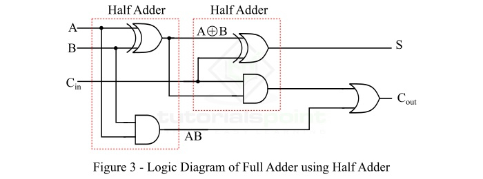
The block diagram of a full adder using two half adders is shown in Figure-4.

From the logic diagram of the full adder using half adders, it is clear that we require two XOR gates, two AND gates and one OR gate for the implementation of a full adder circuit using half-adders.
However, the implementation of full adder using half adder has a major disadvantage that is the increased propagation delay. That means, the input bits must propagate through several gates in succession that increases the total propagation delay of the full adder circuit.
Difference between Half Adder and Full Adder
An adder circuit is one of the important digital circuits used in computers, calculators, digital processing units, etc. There are two types adder circuits named half-adder and full-adder. Both the half adder and the full adder circuits are used to perform addition and also widely used for performing various arithmetic functions in the digital circuits.
What is a Half Adder?
A combinational logic circuit which is designed to add two binary digits is known as half adder. The half adder provides the output along with a carry value (if any). The half adder circuit is designed by connecting an EX-OR gate and one AND gate. It has two input terminals and two output terminals for sum and carry.

In case of half adder, the output of the EX-OR gate is the sum of two bits while the output of the AND gate is the carry. However, the carry obtained is one addition will not be forwarded in the next addition, so it is called half adder.
The output equations of the half adder are −
$$\mathrm{Sum, \: S \: = \: A \oplus{B}}$$
$$\mathrm{Carry, \: C \: = \: A\cdot B}$$
What is a Full Adder?
A combinational circuit which is designed to add three binary digits and produce two outputs is known as full adder. The full adder circuit adds three binary digits, where two are the inputs and one is the carry forwarded from the previous addition.

The circuit of the full adder consists of two EX-OR gates, two AND gates and one OR gate, which are connected together as shown in the full adder circuit.
The output equations of the full adder are −
$$\mathrm{Sum, \: S \: = \: A \oplus{B} \oplus{C_{in}}}$$
$$\mathrm{Carry, \: C \: = \: AB \: + \: BC_{in} \: + \: AC_{in}}$$
Difference Between Half Adder and Full Adder
The following table shows the main differences between half adder and full adder circuit.
| Parameter | Half Adder | Full Adder |
|---|---|---|
| Definition | Half adder is a combinational digital circuit which can add two 1-bit binary numbers. | Full adder is a combinational digital circuit which can add three single-bit binary number, where two are the inputs and the third is the carry forwarded from the previous output. |
| Circuit components | The circuit of the half adder consists of one EX-OR gate and one AND gate. | The circuit of full adder consists of two EX-OR gates, two AND gates and one OR gate. |
| Addition of carry bit | The half adder does not add the carry generated in the previous addition to the next addition. | In case of full adder, the carry produced in the previous addition is added in the next addition. |
| Number of input and output terminals | Half adder circuit has two input terminals viz. A and B and two output terminals, viz. Sum and Carry. | Full adder circuit has three input terminals viz. A, B and Cin and two output terminals, i.e., Sum and Carry. |
| Logical Expressions |
For half adder circuit, the logical expressions of the outputs are − $\mathrm{S \: = \: A \oplus{B}}$ $\mathrm{C \: = \: A\cdot B} $ |
For full adder circuit, the logical expressions of the outputs are − $\mathrm{S \: = \: A \oplus{B} \oplus{C_{in}}}$ $\mathrm{C \: = \: AB \: + \: BC_{in} \: + \: AC_{in}}$ |
| Substitution | A half adder circuit cannot be used as a full adder circuit. | A full adder circuit can substitute a half adder circuit. |
| Design | The circuit of a half adder is simple and easy to implement. | The circuit of a full adder has relatively complex design. |
| Alternate Name | For half adder, there is no alternate name. | Full adder is also called ripple-carry adder. |
| Applications | Half adder circuits are used in computers, calculators, and various digital measuring instruments. | Full adders are mainly used for multiple bit addition, in digital processing devices, etc. |
Conclusion
From the above discussion, it is clear that there are several differences between a half-adder circuit and a full-adder circuit. However, both half adder and full adder circuits are the basic building blocks of many digital circuits that are used to perform arithmetic operations such as calculators, computers, digital measuring devices, digital processors, etc.
One of the main advantage of using half adders and full adders in the digital circuits is that they are designed by using logic gates that process the input data very fast. The typical processing speed of the logic gates is of the order of μs (microseconds). Hence, for performing arithmetic operations at high speed, we use half adder and full adder circuits.
Binary Adder-Subtractor
A binary adder-subtractor is a digital circuit that is used to perform two basic arithmetic operations namely, binary addition and binary subtraction. It is an important component in various digital systems like computers, calculators, etc.
The most significant advantage of using a binary adder-subtractor is that it combines the addition and subtraction operations in a single circuit which results in compact size and lower cost.
Read this chapter to understand the circuit and operation of a binary adder-subtractor.
What is a Binary Adder-Subtractor?
In digital electronics, there is a digital circuit which employed for performing addition and subtraction operations, it is called a binary adder-subtractor.
A binary adder-subtractor is a specially designed digital arithmetic circuit that combines the functionality of addition and subtraction of binary numbers in a single circuit.
A binary adder-subtractor circuit performs the binary addition and subtraction operations on two binary numbers by following the rules given below.
Rules of Binary Addition
The following rules are to be followed while performing binary addition −
| First Bit (A) | Second Bit (B) | Sum (A + B) | Carry |
|---|---|---|---|
| 0 | 0 | 0 | 0 |
| 0 | 1 | 1 | 0 |
| 1 | 0 | 1 | 0 |
| 1 | 1 | 0 | 1 |
Rules of Binary Subtraction
The following table shows the rules to be followed while performing binary subtraction −
| First Bit (A) | Second Bit (B) | Sum (A - B) | Borrow |
|---|---|---|---|
| 0 | 0 | 0 | 0 |
| 0 | 1 | 1 | 1 |
| 1 | 0 | 1 | 0 |
| 1 | 1 | 0 | 0 |
This is all about a basic introduction to binary adder-subtractor and the rules of binary addition and subtraction. Let us now understand the circuit construction of binary adder-subtractor.
Binary Adder-Subtractor Circuit
The logic circuit of a binary adder-subtractor consists of several full-adder circuits connected together. It also consists of a control circuit consisting of XOR gates and performs the mode selection function i.e., the control circuit is used to switch the circuit operation between addition and subtraction.
The circuit diagram of a binary adder-subtractor which can perform the addition or subtraction of two 4-bit binary numbers (say A and B) is shown below −
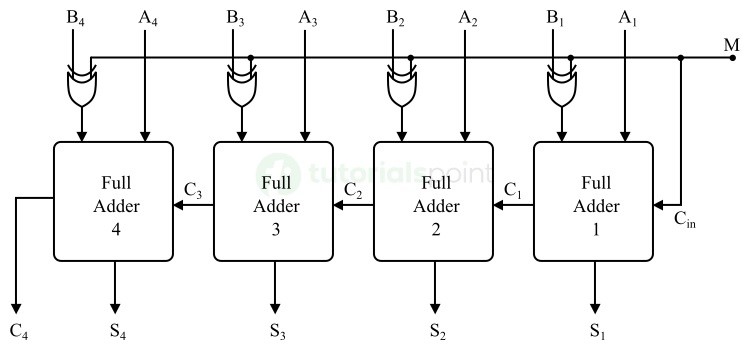
Components of a Binary Adder-Subtractor
The circuit of a binary adder-subtractor consists of the following main components −
Full Adders
A full adder is a binary arithmetic circuit used to perform the addition of three binary bits at a time. It produces two outputs namely a sum and a carry. In a binary adder-subtractor circuit, the full adder circuit can also perform the subtraction operation using the complement mechanism.
Control Circuit
It is a logic circuit used for mode selection i.e., addition mode or subtraction mode. The control circuit of a binary adder-subtractor is designed using XOR gates.
Working of Binary Adder-Subtractor
Let us now understand the operation of a binary adder-subtractor circuit shown in the above figure.
The circuit shown in the above figure is a 4-bit binary adder-subtractor. Therefore, it can perform addition or subtraction of two 4-bit binary numbers, say A and B.
In this circuit, the input M is called the mode input. It controls the operation of the circuit as described below −
- When M = 0, the circuit operates as a binary adder. Under this mode, we get $\mathrm{B_{X} \: \oplus \: 0 \: = \: B_{X}}$. Thus, each full adder receives the inputs Ax and Bx and performs their addition, i.e., Ax + Bx.
- When M = 1, the circuit operates as a binary subtractor. In this case, we get $\mathrm{B_{X} \: \oplus \: 1 \: = \: B_{X}}$ and the input carry Cin = 1. Under this mode, the full adders receive Bx inputs in their complemented form and a 1 is added through the input carry Cin. Hence, the final output of the circuit is Ax + 2s complement of Bx which is the subtraction of Ax and Bx.
This is how the binary adder-subtractor circuit performs both binary addition and binary subtraction operations.
We can conclude the working of a binary adder-subtractor in the following points −
- First of all, select the mode of operation (addition or subtraction) of the circuit. To perform binary addition, set M = 0, and to perform binary subtraction, set M = 1.
- Supply the two input binary numbers to be added or subtracted.
- The circuit will perform the addition or subtraction of input numbers depending on the selected mode and produce a result (either a sum or a difference).
Advantages of Binary Adder-Subtractor
In the field of digital circuit design, it is important to make the circuit compact as much as possible. Since a binary adder-subtractor circuit combines both binary addition and subtraction operations in a single circuit. It results in the following key advantages −
- Reduced circuit complexity
- Compact and simpler system design
- Versatility
- Ability to perform fast and efficient arithmetic operations
- Reduced need for hardware components
- Compatibility with a wide range of digital systems and devices
- Low power consumption, etc.
Limitations of Binary Adder-Subtractor
Binary adder-subtractor has several advantages as listed above. But it also has some disadvantages and limitations.
Some of the key limitations of binary adder-subtractor are listed below −
- A binary adder-subtractor requires more advanced circuit components and algorithms to achieve high precision and accuracy in addition and subtraction operations.
- The functionality of a binary adder-subtractor is limited to addition and subtraction operations only. It requires additional circuitry and algorithms to implement other mathematical operations like multiplication and division.
- The circuit complexity of a binary adder-subtractor is increased significantly when it is designed to perform addition and subtraction of large numbers of bits and floating-point numbers.
- When the number of digits increases in the numbers to be added or subtracted, the circuit becomes slower due to propagation delay.
- A binary adder-subtractor has a limited dynamic range due to which overflow or underflow conditions can occur when dealing with very large or very small numbers respectively.
- Since a binary adder-subtractor uses 2s complement arithmetic to perform binary subtraction. To implement this operation, we require an additional logic circuit which increases the overall complexity of the circuit.
While designing a binary adder-subtractor, we have to take care of all these limitations to ensure higher efficiency and better performance of the circuit.
Applications of Binary Adder-Subtractor
In digital electronics, the binary adder-subtractor finds applications in a variety of digital systems and electronic devices. Some common devices are listed below in which the binary adder-subtractor is used as a crucial component −
- Arithmetic Logic Units − To perform arithmetic and logical operations.
- Microprocessors and Microcontrollers − To perform mathematical computations.
- Communication Systems − To process digital signals and filter operations on binary data.
- Calculators − To perform addition and subtraction operations.
- Control Systems − To perform real-time signal processing and produce feedback and other control signals.
Conclusion
In this chapter, we explained the basic theory and working of binary adder-subtractor. A binary adder-subtractor is a digital electronic circuit that can perform both addition and subtraction of binary numbers. It combines two arithmetic operations (addition and subtraction) into a single circuit and hence reduces the circuit complexity and size of the digital system.
Binary adder-subtractor are widely used in various digital systems and devices such as microprocessors, microcontrollers, calculators, and more.
Digital Electronics - Half Subtractor
In digital electronics, a subtractor is a combinational logic circuit that can perform the subtraction of two number (binary numbers) and produce the difference between them. It is a combinational circuit that means its output depends on its present inputs only. Although, in practice, the subtraction of two binary number is accomplished by taking the 1's or 2's compliment of the subtrahend and adding it to the minuend.
In this way, the subtraction operation of binary numbers can be converted into simple addition operation which makes hardware construction simple and less expensive. There are two types of subtractors namely, Half Subtractor and Full Subtractor.
In this article, we will discuss the half subtractor, its basic definition, circuit diagram, truth table, characteristic equation, etc. So let's begin with the basic definition of half subtractor.
What is a Half-Subtractor?
A half-subtractor is a combinational logic circuit that have two inputs and two outputs (i.e. difference and borrow). The half subtractor produces the difference between the two binary bits at the input and also produces a borrow output (if any). In the subtraction (A-B), A is called as Minuend bit and B is called as Subtrahend bit. The block diagram and logic circuit diagram of the half subtractor is shown in Figure-1.

Hence, from the logic circuit diagram, it is clear that a half subtractor can be realized using an XOR gate together with a NOT gate and an AND gate.
In the half subtractor as shown in figure-1, A and B are the inputs, d and b are the outputs. Where, d indicates the difference and b indicates the borrow output. The borrow output (b) is the signal that tells the next stage that a 1 has been borrowed.
Operation of Half Subtractor
Now, let us understand the operation of the half subtractor circuit. Half subtractor performs its operation to find the difference of two binary digits according to the rules of binary subtraction, which are as follows −
The output borrow of b is zero (0) as long as the minuend bit (A) is greater than or equal to the subtrahend bit (B), i.e. A B. The output borrow is a 1 when A = 0 and B = 1.
From the logic circuit diagram of the half subtractor, it is clear that the difference bit (d) is obtained by the XOR operation of the two inputs A and B, and the borrow bit is obtained by AND operation of the compliment of the minuend (A') with the subtrahend (B).
Truth Table of Half Subtractor
The following is the truth table the half-subtractor −
| Inputs | Outputs | ||
|---|---|---|---|
| A | B | D (Difference) | B (Borrow) |
| 0 | 0 | 0 | 0 |
| 0 | 1 | 1 | 1 |
| 1 | 0 | 1 | 0 |
| 1 | 1 | 0 | 0 |
K-Map for Half Subtractor
We can use the K-Map (or Karnaugh Map), a method for simplifying Boolean algebra, to determine equations of the difference bit (d) and the output borrow (b).
The K-Map simplification for half subtractor is shown in Figure-2.

Characteristic Equation of Half Subtractor
The characteristic equations of the half subtractor, i.e. equations of the difference bit (d) and the output borrow bit (b) are obtained by following the rules of binary subtraction. These equations are given as follows −
The difference bit (d) of the half subtractor is given by XORing the two inputs A and B. Therefore,
$$\mathrm{Difference, \: d \: = \: A \oplus B \: = \: A'B \: + \: AB'}$$
The borrow (b) of the half subtractor is the AND of A (compliment of A) and B. Therefore,
$$\mathrm{Borrow, \: b \: = \: A'B}$$
Applications of Half Subtractor
The following are some important applications of half subtractor −
- Half subtractor is used in ALU (Arithmetic Logic Unit) of processors.
- Half subtractor can also be used in amplifiers to compensate the sound distortion.
- It is also used to decrease the force of radio signals or audio signals.
- Half subtractor is also used to increase or decrease operators.
Conclusion
From the above discussion, we can conclude that a half subtractor is a combinational logic circuit that can calculate the difference of two binary digits. A half subtractor can only be used to subtract the LSB (Least Significant Bit) of the subtrahend from the LSB of the minuend when one binary number is subtracted from another binary number.
Full Subtractor in Digital Electronics
What is a Full-Subtractor?
A full-subtractor is a combinational circuit that has three inputs A, B, bin and two outputs d and b. Where, A is the minuend, B is subtrahend, bin is borrow produced by the previous stage, d is the difference output and b is the borrow output.
As we know that the half-subtractor can only be used for subtraction of LSB (least significant bit) of binary numbers. If there is any borrow during the subtraction of the LSBs of two binary numbers, then it will affect the subtraction of next stages. Therefore, the subtraction with borrow are performed by a full subtractor.
The block diagram and circuit diagram of a full-subtractor is shown in Figure-1.
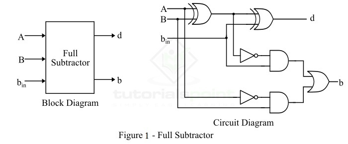
Therefore, we can realize the full-subtractor using two XOR gates, two NOT gates, two AND gates, and one OR gate.
Operation of Full Subtractor
Now, let us understand the operation of the full subtractor. Full subtractor performs its operation to find the difference of two binary numbers according to the rules of binary subtraction, which are as follows −
In the case of full subtractor, the 1s and 0s for the output variables (difference and borrow) are determined from the subtraction of A B bin.
From the logic circuit diagram of the full subtractor, it is clear that the difference bit (d) is obtained by the XOR operation of the two inputs A, B, and bin, and the output borrow bit (b) is obtained by NOT, AND, and OR operations of variable A, B, and bin.
Truth Table of Full-Subtractor
The truth table is one that gives relationship between input and output of a logic circuit. The following is the truth table of the full-subtractor −
| Inputs | Outputs | |||
|---|---|---|---|---|
| A | B | Bin | D (Difference) | B (Borrow) |
| 0 | 0 | 0 | 0 | 0 |
| 0 | 0 | 1 | 1 | 1 |
| 0 | 1 | 0 | 1 | 1 |
| 0 | 1 | 1 | 0 | 1 |
| 1 | 0 | 0 | 1 | 0 |
| 1 | 0 | 1 | 0 | 0 |
| 1 | 1 | 0 | 0 | 0 |
| 1 | 1 | 1 | 1 | 1 |
K-Map for Full Subtractor
We can use the K-Map (or Karnaugh Map), a method for simplifying Boolean algebra, to determine equations of the difference bit (d) and the output borrow bit (b).
The K-Map simplification for half subtractor is shown in Figure-2.
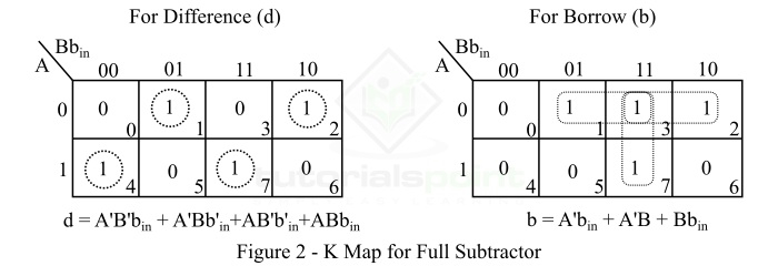
Characteristic Equations of Full Subtractor
The characteristic equations of the full subtractor, i.e. equations of the difference (d) and borrow output (b) are obtained by following the rules of binary subtraction. These equations are given below −
The difference (d) of the full subtractor is the XOR of A, B, and bin. Therefore,
$$\mathrm{Difference, \: d \: = \: A \oplus B \oplus b_{in} \: = \: A'B'b_{in} \: + \: AB'b'_{in} \: + \: A'Bb'_{in} \: + \: ABb_{in}}$$
The borrow (b) of the full subtractor is given by,
From the logic circuit diagram and k-map −
$$\mathrm{Borrow, \: b \: = \: A'B \: + \: \left ( A \oplus B \right ) \: 'b_{in}}$$
From Truth Table
$$\mathrm{Borrow, \: b \: = \: A'B'b_{in} \: + \: A'Bb'_{in} \: + \: A'Bb_{in} \: + \: ABb_{in}}$$
Or
$$\mathrm{Borrow, \: b \: = \: A'B \left ( b_{in} \: + \: b'_{in} \right ) \: + \: \left (AB \: + \: A'B' \right )b_{in} \: = \: A'B \: + \: \left (A \oplus B \right )'b_{in}}$$
Applications of Full Subtractor
The following are some important applications of full subtractor −
- Full subtractors are used in ALU (Arithmetic Logic Unit) in computers CPUs.
- Full subtractors are extensively used to perform arithmetical operations like subtraction in electronic calculators and many other digital devices.
- Full subtractors are used in different microcontrollers for arithmetic subtraction.
- They are used in timers and program counters (PC).
- Full subtractors are also used in processors to compute addresses, tables, etc.
- Full subtractors are also used in DSP (Digital Signal Processing) and networking based systems.
Conclusion
From the above discussion, we can conclude that a full-subtractor is a combinational logic circuit that can compute the difference of three binary digits. In a full subtractor, the borrow (if any) from the previous stage is also used in subtraction operation in the next stages. Therefore, full subtractors are used to perform subtraction of binary numbers having any number of digits.
Parallel Adder and Parallel Subtractor
In digital electronics, adder and subtractor are the two most basic arithmetic combinational circuits. The adder is a combinational arithmetic circuit used to perform addition of two or more binary numbers. Whereas, the subtractor is a combination arithmetic circuit used to perform subtraction of two binary numbers.
Depending on the form in which the addition and subtraction of binary numbers are executed, the adder and subtractor are classified into following types −
- Serial Adder
- Parallel Adder
- Serial Subtractor
- Parallel Subtractor
This tutorial is meant for explaining Parallel Adder and Parallel Subtractor. But before that let us first discuss the rules of Boolean algebra followed to perform the binary addition and subtraction.
Binary Addition
The following rules are followed while performing binary addition −
| Binary Digit A | Binary Digit B | Sum (A + B) | Carry |
|---|---|---|---|
| 0 | 0 | 0 | 0 |
| 0 | 1 | 1 | 0 |
| 1 | 0 | 1 | 0 |
| 1 | 1 | 0 | 1 |
Binary Subtraction
The following rules are to be followed while performing binary subtraction −
| Binary Digit A | Binary Digit B | Difference (A - B) | Borrow |
|---|---|---|---|
| 0 | 0 | 0 | 0 |
| 0 | 1 | 1 | 1 |
| 1 | 0 | 1 | 0 |
| 1 | 1 | 0 | 0 |
Now, let us discuss the parallel adder and parallel subtractor in detail.
What is Parallel Adder?
A digital circuit that adds two binary numbers of any bit length in parallel form and produces the sum of those number in parallel form is called a parallel adder.
A parallel adder basically consists of full adders in a chain form as shown in Figure 1. Here, the output bit of each full adder is connected to the input carry terminal of the next full adder circuit in the chain.

The parallel adder shown in Figure 1 is a 4-bit parallel adder as it can add two binary number of 4 bits. Although, we can design a parallel adder circuit for any number of bits by increasing the number of full adders in the chain.
In the above parallel adder circuit, the bit A is representing the augend bits and B is representing the addend bits. The first input carry bit to the parallel adder is Cin and the output carry bit of the parallel adder is C4. The output sum bits are designated by S. We can also construct a parallel adder in the form of an IC. For example, when the 4-bit parallel adder is formed in the IC form, then it will have four terminals for augend bits, 4 terminals for addend bits, 4 terminals for sum bits, and 2 terminals for input and output carry bits.
Working of Parallel Adder
The parallel adder shown in figure-1 performs the binary addition of two numbers as per the following step −
Step 1 − Firstly, the full adder circuit FA1 adds the bits A1 and B1 along with the input carry bit Cin to produce the sum bit S1, where it is the LSB (Least Significant Bit) of the output sum. At this stage, a carry bit C1 is generated which is transferred to the next full adder circuit in the chain.
Step 2 − The full adder circuit FA2 adds bits A2 and B2 along with the carry bit C1 from the previous addition. It produces the sum bit S2 which is the second bit of the output sum, and a carry bit C2 is also produced which again forwarded to the next full adder FA3.
Step 3 − The full adder circuit FA3 adds inputs bits A3 and B3 along with the carry bit C2 from previous addition to produce sum bit S3 and carry bit C3.
Step 4 − The full adder FA4 adds input bits A4 and B4 along with the carry bit C3 forward from FA3. It generates the last sum bit S4 and a last carry bit C4.
Step 5 − The output sum of the parallel adder is then given by,
$$\mathrm{S_{out} \: = \: C_{4} \: S_{4} \: S_{3} \: S_{2} \: S_{1}}$$
What is Parallel Subtractor?
A digital arithmetic circuit which is used to find the arithmetic difference of two binary numbers in parallel form is called a parallel subtractor.
We can implement a parallel subtractor in several ways such as combining half subtractors and full subtractors, all full subtractors, all full adders, etc. Here, we have realized a 4-bit parallel subtractor using all full adders with subtrahend bit complemented as shown in Figure 2.

This is the 4-bit parallel subtractor, however, we can implement a parallel subtractor by adding any number of full adders in the chain of the circuit shown in figure-2.
The binary subtraction of two binary numbers can be conveniently accomplished by means of 1's or 2's complement. Where, the complement method converts the subtraction operation in simple addition operation.
The 2's complement of binary numbers is obtained by taking the 1's complement and adding 1 to the least significant pair of bits. The 1's complement can be implemented with the help of a NOT gate (inverter).
Working of Parallel Subtractor
The parallel subtractor shown in above figure-2 carries out the subtraction of two binary numbers as per the following steps −
Step 1 − Firstly, the 1's complement of bit B1 obtained using an inverter and a 1 (Cin) are added to obtain the 2's complement of the bit B1. Then, this 2's complemented B1 is further added to A1. This will produce first bit of the output difference designated by S1, and a carry bit C1 which is connected to the input carry of the FA2.
Step 2 − The full adder FA2 uses the input carry bit C1 to add with its input bit A2 and the 2's complement of the input bit B2 to produce the second difference bit (S2) and the carry bit C2.
Step 3 − The full adder FA3 uses the input carry bit C2 to add with its input bit A3 and the 2's complement of the input bit B3 to produce the third difference bit (S3) and the carry bit C3.
Step 4 − Finally, the full adder FA4 uses the carry bit C3 to add with its input bit A4 and the 2's complement of the input bit B4 to produce the last difference bit (S4) and last carry bit C4.
Once all the result bits are produced, they are expressed to give the difference of the two binary numbers as S4S3S2S1 and borrow bit C4.
Conclusion
This is all about parallel adder and parallel subtractor in digital electronics. The most significant advantage of the parallel adder and subtractor is that they perform the arithmetic addition and subtraction of two binary numbers faster as compared to the serial adder and subtractor.
Implementation of a Full Subtractor using Two Half Subtractors
A subtractor is a combinational logic circuit that can perform the subtraction of two numbers (or binary numbers) and produce the difference between them. It is a combinational logic circuit. Therefore, the output of the subtractor depends only on its present inputs.
There are two types of subtractors namely,
- Half Subtractor
- Full Subtractor
Read this tutorial to find out how you can realize a full subtractor using half subtractors. For the implementation of a full subtractor, we require two half subtractors. Let's start with a brief overview of half and full subtractors.
What is a Half Subtractor?
A half-subtractor is a combinational logic circuit that has two inputs and two outputs where one output is difference bit (d) and another is the borrow bit (b). The half subtractor produces the difference between the two binary bits and also produces a borrow output (if any). In the subtraction (A-B), A is called Minuend and B is called Subtrahend bit.
The block diagram and logic circuit diagram of the half subtractor are shown in Figure-1.
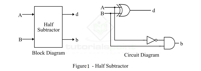
From the logic diagram of the half subtractor, it can be seen that a half subtractor can be realized using an XOR gate together with a NOT gate and an AND gate.
The difference bit (d) of the half subtractor is given by XORing the two inputs A and B. Therefore,
$$\mathbf{Difference,\: d \: = \: A \oplus B \: = \: A'B \: + \: AB'}$$
The borrow (b) of the half subtractor is the AND of A' (compliment of A) and B. Therefore,
$$\mathbf{Borrow, \: b \: = \: A'B}$$
What is a Full Subtractor?
A full subtractor is also a combinational logic circuit which has three inputs A, B, bin and two outputs "d" and "b". Where, "A" is the minuend bit, "B" is the subtrahend bit, "bin" is borrow produced at the previous stage, d is the output difference bit and b is the output borrow bit.
The block diagram and circuit diagram of a full-subtractor is shown in Figure-2.

From the logic diagram of the full subtractor, we can see that the implementation of a fullsubtractor requires two XOR gates, two NOT gates, two AND gates, and one OR gate.
Now, let us discuss the realization of full subtractor using two half subtractors.
Implementation of a Full Subtractor using Two Half Subtractors
A full subtractor can be realized using two half subtractors. It will take two half-subtractors and one OR gate. The logic circuit diagram of the full subtractor using two half subtractors is shown in Figure-3.
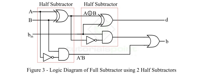
The first half subtractor performs XOR operation on input bits A and B, and AND operation on A' and B to produce an intermediate borrow bit
The second half subtractor performs the XOR operation on the output of first XOR gate and the input borrow bit (bin), and the AND gate of the second half circuit gives an output equal to (A'B + AB')'.bin.
The output of the second XOR gate is the output different bit (d), and the output borrow bit (b) is obtained by ORing the outputs of two AND gates.
In this way, we can realize a full subtractor by cascading two half subtractors, as shown in the above figure
Half Subtractor using NAND Gates
In digital electronics, a subtractor is a combinational logic circuit that performs the subtraction of two binary numbers. However, the subtraction of binary number can be performed using adder circuits by taking 1s or 2s compliments. But, we may also realize a dedicate circuit to perform the subtraction of two binary numbers.
In the subtraction of two binary numbers, each subtrahend bit of the number is subtracted from its corresponding significant minuend bit to form a difference bit. During the subtraction, if the minuend bit is smaller than the subtrahend bit, then a 1 is borrowed from the next position. Depending upon the number of bits taken as input, there are two types of subtractors namely, Half Subtractor and Full Subtractor.
A half subtractor is one which takes two binary digits as input and gives a difference bit and a borrow bit (if any) as output.
On the other hand, a full subtractor is one that takes three bits as input, i.e. two are the input bits and one is the input borrow bit from the previous stage, and gives a difference bit and a output borrow bit as the output.
Since a subtractor is a combinational logic circuit, i.e. it is made of logic gates. We can realize a full adder circuit using different types of logic gates like AND, OR, NOT, NAND, NOR, etc.
Here, we will discuss the implementation of a half subtractor using NAND gates. But before that lets have a look into the basics of the half subtractor.
What is Half Subtractor?
A half-subtractor is a combinational circuit which has two inputs and two outputs where one output is difference and another is borrow bit. The half subtractor produces the difference between the two binary bits at the input and also produces a borrow output (if any). In the subtraction (A-B), A is called as Minuend bit and B is called as Subtrahend bit. The block diagram of the half subtractor is shown in Figure-1.

Here, A and B are the input variables (binary digits) and d is the output difference bit and b is the borrow bit. We can understand the operation of a half subtractor with the help of its truth table.
Truth Table of Half Subtractor
The following is the truth table the half subtractor −
| Inputs | Outputs | ||
|---|---|---|---|
| A | B | D (Difference) | B (Borrow) |
| 0 | 0 | 0 | 0 |
| 0 | 1 | 1 | 1 |
| 1 | 0 | 1 | 0 |
| 1 | 1 | 0 | 0 |
Using this truth table, we can determine the output equation of the half subtractor. The following are the equations of difference bit (d) and borrow bit (b) −
Different Bit (D) −
$$\mathrm{Difference, \: d \: = \: A'B \: + \: AB' \: = \: A \oplus B}$$
Borrow Bit (B)
$$\mathrm{Borrow, \: b \: = \: A'B}$$
Now, let us discuss the realization of half subtractor using NAND gates.
Half Subtractor Using NAND Gates
We may implement the logic circuit of half subtractor using NAND gates only as shown in figure-2.

From this logic circuit diagram, we can see that 9 NAND gates are required for realization of the half subtractor.
The output equations of the half subtractor in NAND logic are as follows −
Difference Bit (D)
$$\mathrm{Difference, \: d \: = \: \overline{\overline{A \cdot \: \overline{AB}} \: \cdot \: \overline{B \cdot \overline{AB}}} \ = \: A \oplus B}$$
Borrow Bit (B)
$$\mathrm{Borrow, \: b \: = \: \overline{\overline{B \cdot \: \overline{AB}}} \: = \: \overline{A} \: B}$$
In this way, we can realize the half subtractor using the NAND gates only.
Digital Electronics - Sequential Circuits
Digital circuits are classified into two major categories namely, combinational circuits and sequential circuits. We have already discussed about combinational circuits in the earlier chapters of this tutorial. This chapter will highlight the details of sequential circuits.
A sequential circuit is a type of digital logic circuit whose output depends on present inputs as well as past operation of the circuit. Let us start this section of the tutorial with a basic introduction to sequential circuits.
What is a Sequential Circuit?
A sequential circuit is a logic circuit that consists of a memory element to store history of past operation of the circuit. Therefore, the output of a sequential circuit depends on present inputs as well as past outputs of the circuit.
The block diagram of a typical sequential circuit is shown in the following figure −

Here, it can be seen that a sequential circuit is basically a combination of a combinational circuit and a memory element. The combinational circuit performs the logical operations specified, while the memory element records the history of operation of the circuit. This history is then used to perform various logical operations in future.
The sequential circuits are named so because they use a series of latest and previous inputs to determine the new output.
Main Components of Sequential Circuit
A sequential circuit consists of several different digital components to process and hold information in the system. Here are some key components of a sequential circuit explained −
Logic Gates
The logic gates like AND, OR, NOT, etc. are used to implement the data processing mechanism of the sequential circuits. These logic gates are basically interconnected in a specific manner to implement combinational circuits to perform logical operations on input data.
Memory Element
In sequential circuits, the memory element is another crucial component that holds history of circuit operation. Generally, flip-flops are used as the memory element in sequential circuits.
In sequential circuits, a feedback path is provided between the output and the input that transfers information from output end to the memory element and from memory element to the input end.
All these components are interconnected together to design a sequential circuit that can perform complex operations and store state information in the memory element.
Types of Sequential Circuits
Based on structure, operation, and applications, the sequential circuits are classified into the following two types −
- Asynchronous Sequential Circuit
- Synchronous Sequential Circuit
Let us discuss both of these sequential circuits in detail.
Asynchrnous Sequential Circuit
A type of sequential circuit whose operation does not depend on the clock signals is known as an asynchronous sequential circuit. This type of sequential circuits operates using the input pulses that means their state changes with the change in the input pulses.
The main components of the asynchronous sequential circuits include un-clocked flip flops and combinational logic circuits. The block diagram of a typical asynchronous sequential circuit is shown in the following figure.
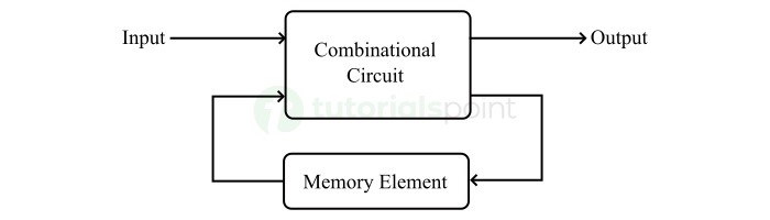
From this diagram, it is clear that an asynchronous sequential circuit is similar to a combinational logic circuit with a feedback mechanism.
Asynchronous sequential circuits are mainly used in applications where the clock signals are not available or practical to use. For example, in conditions when speed of the task execution is important.
Asynchronous sequential circuits are relatively difficult to design and sometimes they produce uncertain output.
The ripple counter is a common example of asynchronous sequential circuit.
Synchronous Sequential Circuit
A synchronous sequential circuit is a type of sequential circuit in which all the memory elements are synchronized by a common clock signal. Hence, synchronous sequential circuits take a clock signal along with input signals.
In synchronous sequential circuits, the duration of the output pulse is equivalent to the duration of the clock pulse applied. Take a look at the block diagram of a typical synchronous sequential circuit −
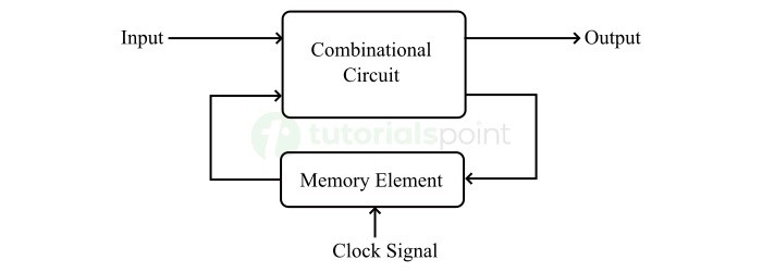
In this figure, it can be seen that the memory element of the sequential circuit is synchronized by a clock signal.
The major disadvantage of the synchronous sequential circuits is that their operation is quite slow. This is because, every time the circuit has to wait for a clock pulse for the operation to take place. However, the most significant advantage of synchronous sequential circuits is that they have a reliable and predictable operation.
Some common examples of synchronous sequential circuits include counters, registers, memory units, control units, etc.
Sequential Circuits vs. Combinational Circuits
Given below is a list of some of the main advantages of using sequential circuits over combinational logic circuits −
- Sequential circuits can retain the operation history which is important in various applications like data storage, feedback control systems, etc.
- Sequential circuits exhibit dynamic behavior and can execute complex operation in real time.
- Sequential circuits comprise a feedback mechanism which improves the stability and optimizes the system performance.
- Synchronous sequential circuits use a common clock signal for synchronization that ensures reliable operation of the circuit.
- Sequential circuits can perform more complex operations using simpler circuit designs than combinational circuits. Hence, their hardware complexity is lesser.
Disadvantages of Sequential Circuits
Sequential circuits do have several disadvantages too. Some of the key disadvantages of using sequential circuits are listed below −
- Sequential circuits have higher propagation delay because the input signal passes through multiple stages of logic circuits and memory elements.
- Sequential circuits are relatively complicated and time taking process to design and analyze.
- Sequential circuits require a proper synchronization and clock distribution to work as intended.
- As compared to combinational circuits, sequential circuits consume relatively more power due to complex design and use of additional components like clock and memory element.
Applications of Sequential Circuits
Sequential circuits are used in a wide range of applications in the field of digital electronics.The following are some common examples of applications of sequential circuits −
- Sequential circuits are used in digital counters employed in applications like frequency division, event counting, time keeping, and more.
- Sequential circuits are also used in digital memory devices like flip-flops, registers, etc. to store and retrieve data.
- Sequential circuits are used to design control circuits in digital systems.
- Sequential circuits play an important role in sequential logic and state-based data processing operations.
- Sequential circuits are also used in automation systems to control the operation of machines based on predefined logics.
- In communication systems, sequential circuits are used to implement communication protocols and data transmission standards.
Conclusion
Sequential circuits are important components in digital electronic systems. A sequential circuit is nothing but a combination of combinational logic circuit and a memory element, where the memory element is connected in a feedback mechanism with the combinational circuit.
The most important thing to be noted about sequential circuits is that their output is determined by both present inputs and previous inputs and outputs.
Sequential circuits are used to design complex digital systems that can perform advance operations like real-time data processing, storage and transmission of data, counting events, and more.
Clock Signal and Triggering
In this chapter, let us discuss about the clock signal and types of triggering one by one.
Clock Signal
Clock signal is a periodic signal and its ON time and OFF time need not be the same. We can represent the clock signal as a square wave, when both its ON time and OFF time are same. This clock signal is shown in the following figure.
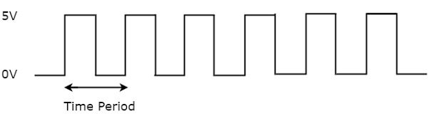
In the above figure, square wave is considered as clock signal. This signal stays at logic High (5V) for some time and stays at logic Low (0V) for equal amount of time. This pattern repeats with some time period. In this case, the time period will be equal to either twice of ON time or twice of OFF time.
We can represent the clock signal as train of pulses, when ON time and OFF time are not same. This clock signal is shown in the following figure.
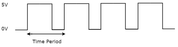
In the above figure, train of pulses is considered as clock signal. This signal stays at logic High (5V) for some time and stays at logic Low (0V) for some other time. This pattern repeats with some time period. In this case, the time period will be equal to sum of ON time and OFF time.
The reciprocal of the time period of clock signal is known as the frequency of the clock signal. All sequential circuits are operated with clock signal. So, the frequency at which the sequential circuits can be operated accordingly the clock signal frequency has to be chosen.
Types of Triggering
Following are the two possible types of triggering that are used in sequential circuits.
- Level Triggering
- Edge Triggering
Level Triggering
There are two levels, namely logic High and logic Low in clock signal. Following are the two types of level triggering.
- Positive Level Triggering
- Negative Level Triggering
If the sequential circuit is operated with the clock signal when it is in Logic High, then that type of triggering is known as Positive level triggering. It is highlighted in below figure.
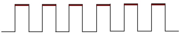
If the sequential circuit is operated with the clock signal when it is in Logic Low, then that type of triggering is known as Negative level triggering. It is highlighted in the following figure.

Edge Triggering
There are two types of transitions that occur in clock signal. That means, the clock signal transitions either from Logic Low to Logic High or Logic High to Logic Low.
Following are the two types of edge triggering based on the transitions of clock signal.
- Positive Edge Triggering
- Negative Edge Triggering
Positive Edge Triggering
If the sequential circuit is operated with the clock signal that is transitioning from Logic Low to Logic High, then that type of triggering is known as Positive Edge Triggering. It is also called as rising edge triggering. It is shown in the following figure.
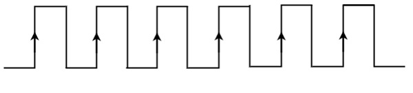
Negative Edge Triggering
If the sequential circuit is operated with the clock signal that is transitioning from Logic High to Logic Low, then that type of triggering is known as Negative Edge Triggering. It is also called as falling edge triggering. It is shown in the following figure.
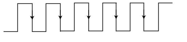
In the coming chapters, we will discuss about various sequential circuits based on the type of triggering that can be used in it.
Digital Electronics - Latches
A latch is an asynchronous sequential circuit whose output changes immediately with the change in the applied input. A latch is used to store 1 bit information in a digital system, so it is considered as the most elementary memory element.
In this chapter, we will explain in detail about latches in digital electronics along with their types and applications.
What is a Latch?
In digital electronics, a latch is an asynchronous sequential circuit that can store 1-bit information. It is used as the fundamental memory element in digital circuits.
A latch can have two stable states namely, set and reset. The set state is denoted by the logic 1 and the reset state is represented by the logic 0. Due to these two stable states, a latch is also known as a bistable-multivibrator. The state of a latch toggles according to the applied input.
The most important thing to be noted about latches is that they do not have a clock signal for synchronization. That is why they are called asynchronous sequential circuits.
The logic gates are the fundamental building blocks of latches. Since there is no synchronization and clock signal used. Hence, the latches operate immediately on the application of input signals.
Characteristics of Latches
Some key characteristics of latches are explained below −
- Latches can store 1-bit of digital information that can be represented using either logic 0 or logic 1. Thus, the latches are mainly used as memory elements in digital circuits.
- Latches have a feedback mechanism that allows them to maintain their current state as it is until the next input is applied.
- The operation of latches is completely controlled by applied inputs that means the output of the latches updates based on the change in the input signals.
Types of Latches
The following are the main types of latches that used in digital circuits and systems −
- SR Latch
- JK Latch
- D Latch
- T Latch
Let us now discuss about each type of latch in detail.
SR Latch
The SR latch is a type of latch which has two input lines designated as S and R. Where, S represents the Set input and R represents the Reset input. Thus, it is also known as Set-Reset Latch.
The SR latch has two stable states namely Set state (S) and Reset state (R). The block diagram of the SR latch is shown in the following figure.
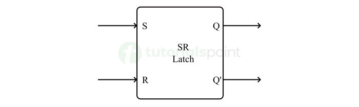
In the case of SR latch, the S input sets the output Q to 1 and Q' to 0. On the other hand, the R input sets the output Q to 0 and Q' to 1. In case, when both S and R inputs are high, the latch is said to be in forbidden state.
The complete operation of the SR latch for different input combinations is described in the following truth table −
| Inputs | Outputs | Comment | ||
|---|---|---|---|---|
| S | R | Q | Q' | |
| 0 | 0 | Q | Q' | No change |
| 0 | 1 | 0 | 1 | Reset state |
| 1 | 0 | 1 | 0 | Set state |
| 1 | 1 | X | X | Forbidden state |
The SR latch can be implemented by connecting two NOR gates in a cross-coupled manner as shown in the following figure.

JK Latch
The JK latch is another type of latch which has two inputs namely, J and K. Here, the input J is similar to S input and the input K is similar to R input in an SR latch.
The operation of the JK latch is similar to that of the SR latch but it does not have the forbidden state. Instead, it has a toggle state in which the outputs Q and Q' swap their states when both inputs J and K are 1.
Therefor, the JK latch is mainly designed to overcome the problem of forbidden state in the SR latch.
The block diagram of the JK latch is shown in the following figure −
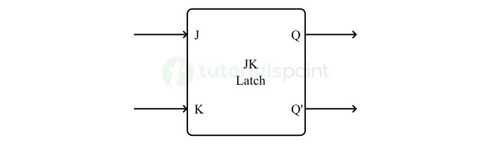
The truth table given below describes the operation of the JK latch for different input combinations −
| Inputs | Outputs | Comment | ||
|---|---|---|---|---|
| J | K | Q | Q' | |
| 0 | 0 | Q | Q' | No change |
| 0 | 1 | 0 | 1 | Reset state |
| 1 | 0 | 1 | 0 | Set state |
| 1 | 1 | Q' | Q | Toggle state |
From this truth table, it is clear that the problem of forbidden state is addressed by implementing the toggle state.
The logic circuit of the JK latch consists of a combination of two NOR gates and two AND gates as shown in the following figure.
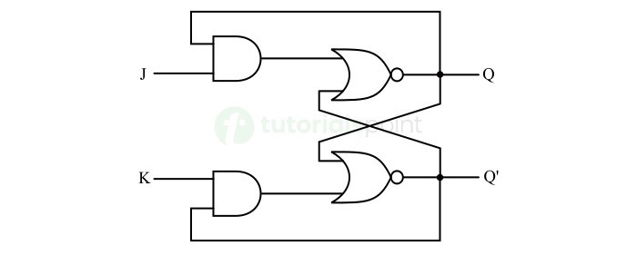
D Latch
The D Latch, also known as Data latch or transparent latch, is a type of bistable multivibrator which has two input signals namely, D (Data) input and E (Enable) input.
The output Q of the D latch is same as the input applied at the D input line as long as the E input is high. When the E input goes low, the output of the D latch is held as it is until the new input is applied to the D input.
The block diagram of the D latch is shown in the following figure.
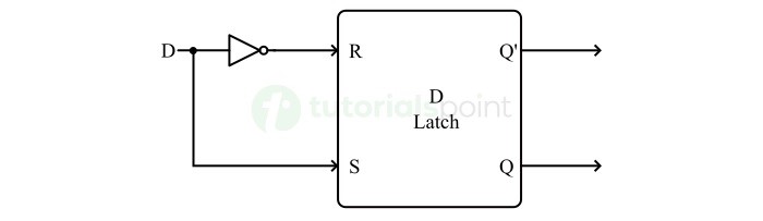
The truth table given below explains the operation of the D latch −
| Inputs | Outputs | Comment | ||
|---|---|---|---|---|
| D | E | Q | Q' | |
| 0 | 0 | Q | Q' | No change |
| 0 | 1 | 0 | 1 | Reset state |
| 1 | 0 | Q | Q' | No change |
| 1 | 1 | 1 | 0 | Set state |
The logic circuit diagram of the D latch is depicted in the following figure −
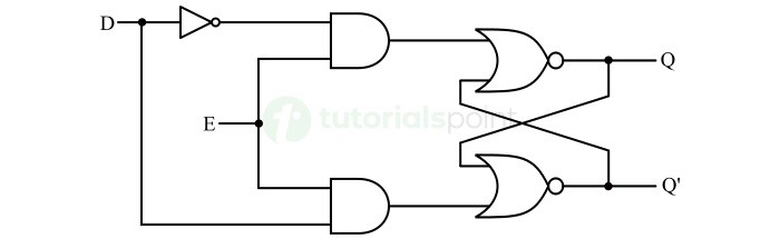
T Latch
T latch is a type of latch that toggles its output state (Q) when a logic 1 is applied to its input line. Hence, it is also known as toggle latch.
The T latch is implemented by connecting the J and K inputs of the JK latch together as shown in the following block diagram.
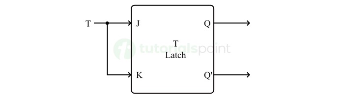
The truth table describing the operation of the T latch is shown below −
| Input | Present State | Next State | ||
|---|---|---|---|---|
| T | Q | Q' | Q | Q' |
| 0 | 0 | 1 | 0 | 1 |
| 0 | 1 | 0 | 1 | 0 |
| 1 | 0 | 1 | 1 | 0 |
| 1 | 1 | 0 | 0 | 1 |
The logic circuit diagram of the T latch is shown in the following figure −
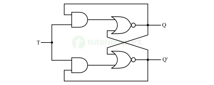
Applications of Latches
The latches find several applications in the field of digital electronics. They are most elementary storage components used to store one bit of information in digital systems.
Some of the common applications of latches are listed here −
- Latches are used as 1-bit memory element in digital systems.
- Latches are used to design digital registers which are employed for storage and manipulation of data in microprocessors and microcontrollers.
- Latches are used to design flip-flops which are basically the synchronized latches.
- Latches are also used in communication systems for temporary data storage or buffering purposes.
Conclusion
In this chapter, we explained different types of latches used in digital systems along with some examples of applications of latches.
In conclusion, a latch is a 1-bit storage device made up of logic gates. It is a type of asynchronous sequential logic circuit which do not have a clocked signal for synchronization.
In digital systems, latches are used to serve some key functions like temporary data storage, data flow control, etc.
Digital Electronics - Flip-Flops
A flip-flop is a sequential digital electronic circuit having two stable states that can be used to store one bit of binary data. Flip-flops are the fundamental building blocks of all memory devices.
Types of Flip-Flops
- S-R Flip-Flop
- J-K Flip-Flop
- D Flip-Flop
- T Flip-Flop
S-R Flip-Flop
This is the simplest flip-flop circuit. It has a set input (S) and a reset input (R). When in this circuit when S is set as active, the output Q would be high and the Q' will be low. If R is set to active then the output Q is low and the Q' is high. Once the outputs are established, the results of the circuit are maintained until S or R get changed, or the power is turned off.
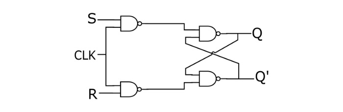
Truth Table of S-R Flip-Flop
| S | R | Q | State |
|---|---|---|---|
| 0 | 0 | 0 | No Change |
| 0 | 1 | 0 | Reset |
| 1 | 0 | 1 | Set |
| 1 | 1 | X |
Characteristics Table of S-R Flip-Flop
| S | R | Q(t) | Q(t+1) |
|---|---|---|---|
| 0 | 0 | 0 | 0 |
| 0 | 0 | 1 | 1 |
| 0 | 1 | 0 | 0 |
| 0 | 1 | 1 | 0 |
| 1 | 0 | 0 | 1 |
| 1 | 0 | 1 | 1 |
| 1 | 1 | 0 | X |
| 1 | 1 | 1 | X |
Characteristics Equation of S-R Flip-Flop
$$\mathrm{Q(t \: + \: 1) \: = \: S \: + \: R' \: Q(t)}$$
J-K Flip-Flop
Because of the invalid state corresponding to S=R=1 in the SR flip-flop, there is a need of another flip-flop. The JK flip-flop operates with only positive or negative clock transitions. The operation of the JK flip-flop is similar to the SR flip-flop. When the input J and K are different then the output Q takes the value of J at the next clock edge.
When J and K both are low then NO change occurs at the output. If both J and K are high, then at the clock edge, the output will toggle from one state to the other.
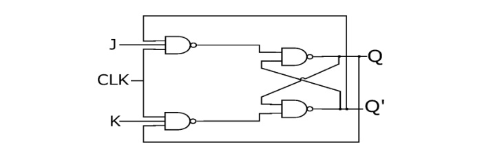
Truth Table of JK Flip-Flop
| J | K | Q | State |
|---|---|---|---|
| 0 | 0 | 0 | No Change |
| 0 | 1 | 0 | Reset |
| 1 | 0 | 1 | Set |
| 1 | 1 | Toggles | Toggle |
Characteristics Table of JK Flip-Flop
| J | K | Q(t) | Q(t+1) |
|---|---|---|---|
| 0 | 0 | 0 | 0 |
| 0 | 0 | 1 | 1 |
| 0 | 1 | 0 | 0 |
| 0 | 1 | 1 | 0 |
| 1 | 0 | 0 | 1 |
| 1 | 0 | 1 | 1 |
| 1 | 1 | 0 | 1 |
| 1 | 1 | 1 | 0 |
Characteristics Equation of JK Flip-Flop
$$\mathrm{Q(t \: + \: 1) \: = \: j \: k \: Q(t)' \: + \: K'Q(t)}$$
D Flip-Flop
In a D flip-flop, the output can only be changed at positive or negative clock transitions, and when the inputs changed at other times, the output will remain unaffected. The D flip-flops are generally used for shift-registers and counters. The change in output state of D flip-flop depends upon the active transition of clock. The output (Q) is same as input and changes only at active transition of clock
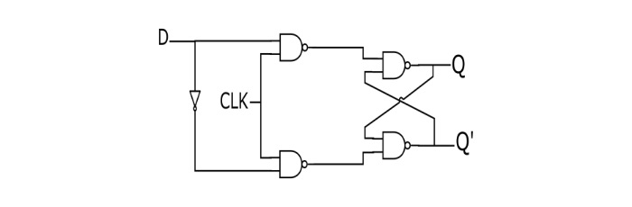
Truth Table of D Flip-Flop
| D | Q |
|---|---|
| 0 | 0 |
| 1 | 1 |
Characteristics Equation of D Flip-Flops
$$\mathrm{Q(t \: + \: 1) \: = \: D}$$
T Flip-Flop
A T flip-flop (Toggle Flip-flop) is a simplified version of JK flip-flop. The T flop is obtained by connecting the J and K inputs together. The flip-flop has one input terminal and clock input. These flip-flops are said to be T flip-flops because of their ability to toggle the input state. Toggle flip-flops are mostly used in counters.

Truth Table of T Flip-Flop
| T | Q(t) | Q(t+1) |
|---|---|---|
| 0 | 0 | 0 |
| 0 | 1 | 1 |
| 1 | 0 | 1 |
| 1 | 1 | 0 |
Characteristics Equation of T Flip-Flop
$$\mathrm{Q(t \: + \: 1) \: = \: T'Q(t) \: + \: TQ(t)' \: = \: T \: \oplus \: Q(t)}$$
Applications of Flip-Flops
- Counters
- Shift Registers
- Storage Registers, etc.
Digital Electronics - Conversion of Flip-Flops
In previous chapter, we discussed the four flip-flops, namely SR flip-flop, D flip-flop, JK flip-flop & T flip-flop. We can convert one flip-flop into the remaining three flip-flops by including some additional logic. So, there will be total of twelve flip-flop conversions.
Follow these steps for converting one flip-flop to the other.
- Consider the characteristic table of desired flip-flop.
- Fill the excitation values (inputs) of given flip-flop for each combination of present state and next state. The excitation table for all flip-flops is shown below.
| Present State | Next State | SR Flip-Flop Inputs | D flip-flop input | JK Flip-Flop Inputs | T Flip-Flop Input | ||
|---|---|---|---|---|---|---|---|
| Q(t) | Q(t+1) | S | R | D | J | K | T |
| 0 | 0 | 0 | x | 0 | 0 | x | 0 |
| 0 | 1 | 1 | 0 | 1 | 1 | x | 1 |
| 1 | 0 | 0 | 1 | 0 | x | 1 | 1 |
| 1 | 1 | x | 0 | 1 | x | 0 | 0 |
Get the simplified expressions for each excitation input. If necessary, use Kmaps for simplifying.
Draw the circuit diagram of desired flip-flop according to the simplified expressions using given flip-flop and necessary logic gates.
Now, let us convert few flip-flops into other. Follow the same process for remaining flipflop conversions.
SR Flip-Flop to other Flip-Flop Conversions
Following are the three possible conversions of SR flip-flop to other flip-flops.
- SR Flip-Flop to D Flip-Flop
- SR Flip-Flop to JK Flip-Flop
- SR Flip-Flop to T Flip-Flop
SR Flip-Flop to D Flip-Flop Conversion
Here, the given flip-flop is SR flip-flop and the desired flip-flop is D flip-flop. Therefore, consider the following characteristic table of D flip-flop.
| D Flip-Flop Input | Present State | Next State |
|---|---|---|
| D | Q(t) | Q(t + 1) |
| 0 | 0 | 0 |
| 0 | 1 | 0 |
| 1 | 0 | 1 |
| 1 | 1 | 1 |
We know that SR flip-flop has two inputs S & R. So, write down the excitation values of SR flip-flop for each combination of present state and next state values. The following table shows the characteristic table of D flip-flop along with the excitation inputs of SR flip-flop.
| D Flip-Flop Input | Present State | Next State | SR Flip-Flop Inputs | |
|---|---|---|---|---|
| D | Q(t) | Q(t + 1) | S | R |
| 0 | 0 | 0 | 0 | x |
| 0 | 1 | 0 | 0 | 1 |
| 1 | 0 | 1 | 1 | 0 |
| 1 | 1 | 1 | x | 0 |
From the above table, we can write the Boolean functions for each input as below.
$$\mathrm{S \: = \: m_{2} \: + \: d_{3}}$$
$$\mathrm{R \: = \: m_{1} \: + \: d_{0}}$$
We can use 2 variable K-Maps for getting simplified expressions for these inputs. The k-Maps for S & R are shown below.
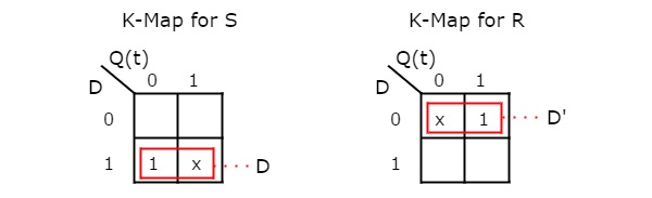
So, we got S = D & R = D' after simplifying. The circuit diagram of D flip-flop is shown in the following figure.
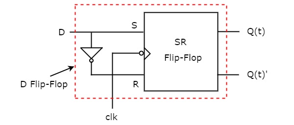
This circuit consists of SR flip-flop and an inverter. This inverter produces an output, which is complement of input, D. So, the overall circuit has single input, D and two outputs Q(t) & Q(t)'. Hence, it is a D flip-flop. Similarly, you can do other two conversions.
D Flip-Flop to other Flip-Flop Conversions
Following are the three possible conversions of D flip-flop to other flip-flops.
- D Flip-Flop to T Flip-Flop
- D Flip-Flop to SR Flip-Flop
- D Flip-Flop to JK Flip-Flop
D Flip-Flop to T Flip-Flop conversion
Here, the given flip-flop is D flip-flop and the desired flip-flop is T flip-flop. Therefore, consider the following characteristic table of T flip-flop.
| T Flip-Flop Input | Present State | Next State |
|---|---|---|
| T | Q(t) | Q(t + 1) |
| 0 | 0 | 0 |
| 0 | 1 | 1 |
| 1 | 0 | 1 |
| 1 | 1 | 0 |
We know that D flip-flop has single input D. So, write down the excitation values of D flip-flop for each combination of present state and next state values. The following table shows the characteristic table of T flip-flop along with the excitation input of D flip-flop.
| T Flip-Flop Input | Present State | Next State | D Flip-Flop Input |
|---|---|---|---|
| T | Q(t) | Q(t + 1) | D |
| 0 | 0 | 0 | 0 |
| 0 | 1 | 1 | 1 |
| 1 | 0 | 1 | 1 |
| 1 | 1 | 0 | 0 |
From the above table, we can directly write the Boolean function of D as below.
$$\mathrm{D \: = \: T \: \oplus \: Q \: \left ( t \: \right )}$$
So, we require a two input Exclusive-OR gate along with D flip-flop. The circuit diagram of T flip-flop is shown in the following figure.

This circuit consists of D flip-flop and an Exclusive-OR gate. This Exclusive-OR gate produces an output, which is Ex-OR of T and Q(t). So, the overall circuit has single input, T and two outputs Q(t) & Q(t). Hence, it is a T flip-flop. Similarly, you can do other two conversions.
JK Flip-Flop to other Flip-Flop Conversions
Following are the three possible conversions of JK flip-flop to other flip-flops.
- JK Flip-Flop to T Flip-Flop
- JK Flip-Flop to D Flip-Flop
- JK Flip-Flop to SR Flip-Flop
JK Flip-Flop to T Flip-Flop conversion
Here, the given flip-flop is JK flip-flop and the desired flip-flop is T flip-flop. Therefore, consider the following characteristic table of T flip-flop.
| T Flip-Flop Input | Present State | Next State |
|---|---|---|
| T | Q(t) | Q(t + 1) |
| 0 | 0 | 0 |
| 0 | 1 | 1 |
| 1 | 0 | 1 |
| 1 | 1 | 0 |
We know that JK flip-flop has two inputs J & K. So, write down the excitation values of JK flip-flop for each combination of present state and next state values. The following table shows the characteristic table of T flip-flop along with the excitation inputs of JK flipflop.
| T Flip-Flop Input | Present State | Next State | JK Flip-Flop Inputs | |
|---|---|---|---|---|
| T | Q(t) | Q(t + 1) | J | K |
| 0 | 0 | 0 | 0 | x |
| 0 | 1 | 1 | x | 0 |
| 1 | 0 | 1 | 1 | x |
| 1 | 1 | 0 | x | 1 |
From the above table, we can write the Boolean functions for each input as below.
$$\mathrm{J \: = \: m_{2} \: + \: d_{1} \: + \: d_{3}}$$
$$\mathrm{K \: = \: m_{3} \: + \: d_{0} \: + \: d_{2}}$$
We can use 2 variable K-Maps for getting simplified expressions for these two inputs. The k-Maps for J & K are shown below.
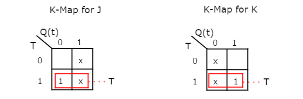
So, we got, J = T & K = T after simplifying. The circuit diagram of T flip-flop is shown in the following figure.
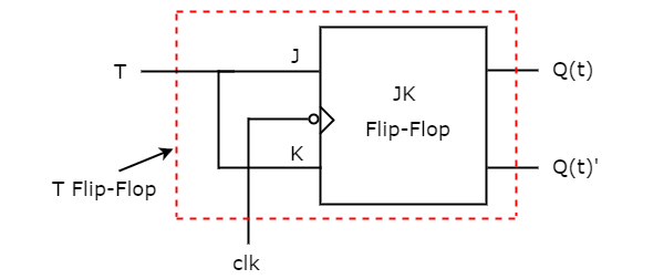
This circuit consists of JK flip-flop only. It doesnt require any other gates. Just connect the same input T to both J & K. So, the overall circuit has single input, T and two outputs Q(t) & Q(t). Hence, it is a T flip-flop. Similarly, you can do other two conversions.
T Flip-Flop to other Flip-Flop Conversions
Following are the three possible conversions of T flip-flop to other flip-flops.
- T Flip-Flop to D Flip-Flop
- T Flip-Flop to SR Flip-Flop
- T Flip-Flop to JK Flip-Flop
T Flip-Flop to D Flip-Flop conversion
Here, the given flip-flop is T flip-flop and the desired flip-flop is D flip-flop. Therefore, consider the characteristic table of D flip-flop and write down the excitation values of T flip-flop for each combination of present state and next state values. The following table shows the characteristic table of D flip-flop along with the excitation input of T flip-flop.
| D Flip-Flop Input | Present State | Next State | T Flip-Flop Input | |
|---|---|---|---|---|
| D | Q(t) | Q(t + 1) | T | |
| 0 | 0 | 0 | 0 | |
| 0 | 1 | 0 | 1 | |
| 1 | 0 | 1 | 1 | |
| 1 | 1 | 1 | 0 | |
From the above table, we can directly write the Boolean function of T as below.
$$\mathrm{T \: = \: D \: \oplus \: Q \left ( t \right )}$$
So, we require a two input Exclusive-OR gate along with T flip-flop. The circuit diagram of D flip-flop is shown in the following figure.
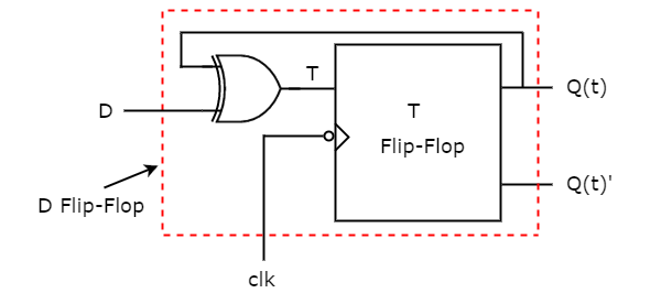
This circuit consists of T flip-flop and an Exclusive-OR gate. This Exclusive-OR gate produces an output, which is Ex-OR of D and Q(t). So, the overall circuit has single input, D and two outputs Q(t) & Q(t). Hence, it is a D flip-flop. Similarly, you can do other two conversions.
Digital Electronics - Shift Registers
Flip-flop is a 1 bit memory cell which can be used for storing the digital data. To increase the storage capacity in terms of number of bits, we have to use a group of flip-flop. Such a group of flip-flop is known as a Register. The n-bit register will consist of n number of flip-flop and it is capable of storing an n-bit word.
The binary data in a register can be moved within the register from one flip-flop to another. The registers that allow such data transfers are called as shift registers. There are four mode of operations of a shift register.
- Serial In - Serial Out (SISO) Shift Register
- Serial In - Parallel Out (SIPO) Shift Register
- Parallel In - Serial Out (PISO) Shift Register
- Parallel In - Parallel Out (PIPO) Shift Register
Serial In - Serial Out (SISO) Shift Register
Let all the flip-flop be initially in the reset condition i.e. Q3 = Q2 = Q1 = Q0 = 0. If an entry of a four bit binary number 1 1 1 1 is made into the register, this number should be applied to Din bit with the LSB bit applied first. The D input of FF-3 i.e. D3 is connected to serial data input Din. Output of FF-3 i.e. Q3 is connected to the input of the next flip-flop i.e. D2 and so on.
Block Diagram
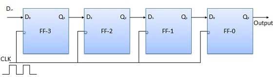
Operation
Before application of clock signal, let Q3 Q2 Q1 Q0 = 0000 and apply LSB bit of the number to be entered to Din. So Din = D3 = 1. Apply the clock. On the first falling edge of clock, the FF-3 is set, and stored word in the register is Q3 Q2 Q1 Q0 = 1000.
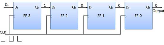
Apply the next bit to Din. So Din = 1. As soon as the next negative edge of the clock hits, FF-2 will set and the stored word change to Q3 Q2 Q1 Q0 = 1100.
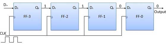
Apply the next bit to be stored i.e. 1 to Din. Apply the clock pulse. As soon as the third negative clock edge hits, FF-1 will be set and output will be modified to Q3 Q2 Q1 Q0 = 1110.
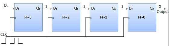
Similarly with Din = 1 and with the fourth negative clock edge arriving, the stored word in the register is Q3 Q2 Q1 Q0 = 1111.
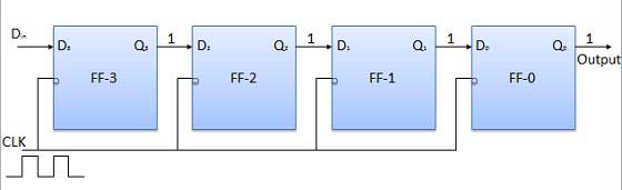
Truth Table
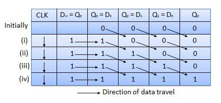
Waveforms
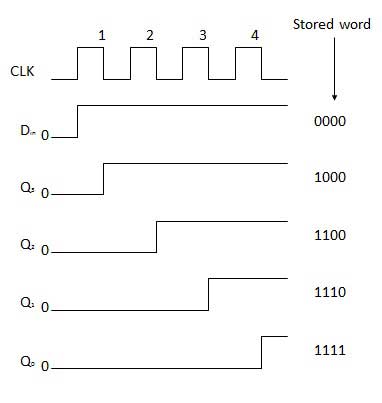
Serial In - Parallel Out (SIPO) Shift Register
- In such types of operations, the data is entered serially and taken out in parallel fashion.
- Data is loaded bit by bit. The outputs are disabled as long as the data is loading.
- As soon as the data loading gets completed, all the flip-flops contain their required data, the outputs are enabled so that all the loaded data is made available over all the output lines at the same time.
- 4 clock cycles are required to load a four bit word. Hence the speed of operation of SIPO mode is same as that of SISO mode.
Block Diagram
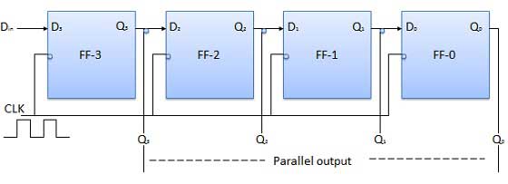
Parallel In - Serial Out (PISO) Shift Register
- Data bits are entered in parallel fashion.
- The circuit shown below is a four bit parallel input serial output register.
- Output of previous Flip Flop is connected to the input of the next one via a combinational circuit.
- The binary input word B0, B1, B2, B3 is applied though the same combinational circuit.
- There are two modes in which this circuit can work namely - shift mode or load mode.
Load Mode
When the shift/load bar line is low (0), the AND gate 2, 4 and 6 become active they will pass B1, B2, B3 bits to the corresponding flip-flops. On the low going edge of clock, the binary input B0, B1, B2, B3 will get loaded into the corresponding flip-flops. Thus parallel loading takes place.
Shift Mode
When the shift/load bar line is low (1), the AND gate 2, 4 and 6 become inactive. Hence the parallel loading of the data becomes impossible. But the AND gate 1,3 and 5 become active. Therefore the shifting of data from left to right bit by bit on application of clock pulses. Thus the parallel in serial out operation takes place.
Block Diagram
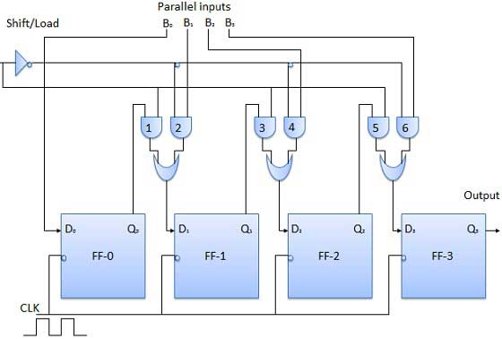
Parallel In - Parallel Out (PIPO) Shift Register
In this mode, the 4 bit binary input B0, B1, B2, B3 is applied to the data inputs D0, D1, D2, D3 respectively of the four flip-flops. As soon as a negative clock edge is applied, the input binary bits will be loaded into the flip-flops simultaneously. The loaded bits will appear simultaneously to the output side. Only clock pulse is essential to load all the bits.
Block Diagram
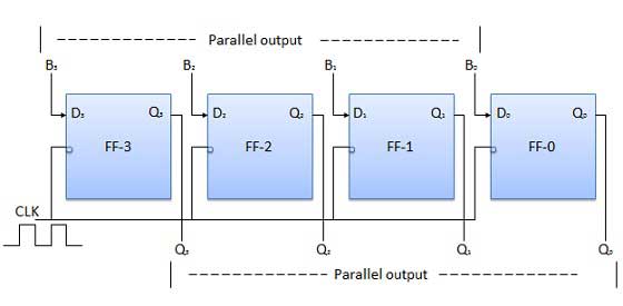
Bidirectional Shift Register
- If a binary number is shifted left by one position then it is equivalent to multiplying the original number by 2. Similarly if a binary number is shifted right by one position then it is equivalent to dividing the original number by 2.
- Hence if we want to use the shift register to multiply and divide the given binary number, then we should be able to move the data in either left or right direction.
- Such a register is called bi-directional register. A four bit bi-directional shift register is shown in fig.
- There are two serial inputs namely the serial right shift data input DR, and the serial left shift data input DL along with a mode select input (M).
Block Diagram
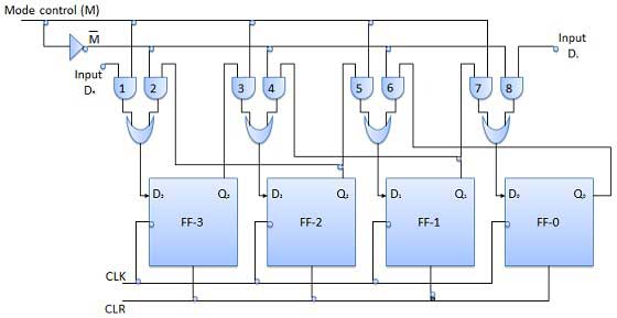
Operation
| Sr.No | Condition | Operation |
|---|---|---|
| 1 | With M = 1 − Shift right operation |
If M = 1, then the AND gates 1, 3, 5 and 7 are enabled whereas the remaining AND gates 2, 4, 6 and 8 will be disabled. The data at DR is shifted to right bit by bit from FF-3 to FF-0 on the application of clock pulses. Thus with M = 1 we get the serial right shift operation. |
| 2 | With M = 0 − Shift left operation |
When the mode control M is connected to 0 then the AND gates 2, 4, 6 and 8 are enabled while 1, 3, 5 and 7 are disabled. The data at DL is shifted left bit by bit from FF-0 to FF-3 on the application of clock pulses. Thus with M = 0 we get the serial right shift operation. |
Universal Shift Register
A shift register which can shift the data in only one direction is called a uni-directional shift register. A shift register which can shift the data in both directions is called a bi-directional shift register. Applying the same logic, a shift register which can shift the data in both directions as well as load it parallely, is known as a universal shift register. The shift register is capable of performing the following operation −
- Parallel Loading
- Left Shifting
- Right Shifting
The mode control input is connected to logic 1 for parallel loading operation whereas it is connected to 0 for serial shifting. With mode control pin connected to ground, the universal shift register acts as a bi-directional register. For serial left operation, the input is applied to the serial input which goes to AND gate-1 shown in figure. Whereas for the shift right operation, the serial input is applied to D input.
Block Diagram
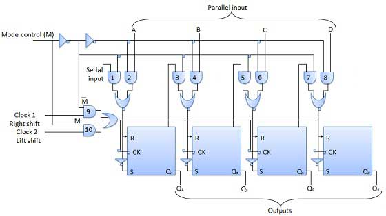
Application of Shift Registers
In previous chapter, we discussed four types of shift registers. Based on the requirement, we can use one of those shift registers. Following are the applications of shift registers.
Shift register is used as Parallel to serial converter, which converts the parallel data into serial data. It is utilized at the transmitter section after Analog to Digital Converter (ADC) block.
Shift register is used as Serial to parallel converter, which converts the serial data into parallel data. It is utilized at the receiver section before Digital to Analog Converter (DAC) block.
Shift register along with some additional gate(s) generate the sequence of zeros and ones. Hence, it is used as sequence generator.
Shift registers are also used as counters. There are two types of counters based on the type of output from right most D flip-flop is connected to the serial input. Those are Ring counter and Johnson Ring counter.
In this chapter, let us discuss about these two counters one by one.
Ring Counter
In previous chapter, we discussed the operation of Serial In - Parallel Out (SIPO) shift register. It accepts the data from outside in serial form and it requires N clock pulses in order to shift N bit data.
Similarly, N bit Ring counter performs the similar operation. But, the only difference is that the output of rightmost D flip-flop is given as input of leftmost D flip-flop instead of applying data from outside. Therefore, Ring counter produces a sequence of states (pattern of zeros and ones) and it repeats for every N clock cycles.
The block diagram of 3-bit Ring counter is shown in the following figure.
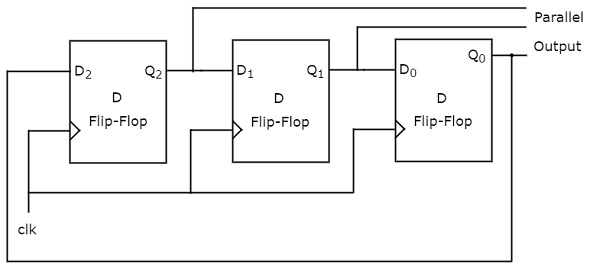
The 3-bit Ring counter contains only a 3-bit SIPO shift register. The output of rightmost D flip-flop is connected to serial input of left most D flip-flop.
Assume, initial status of the D flip-flops from leftmost to rightmost is $\mathrm{Q_{2}Q_{1}Q_{0} \: = \: 001}$. Here, $\mathrm{Q_{2}}$ & $\mathrm{Q_{0}}$ are MSB & LSB respectively. We can understand the working of Ring counter from the following table.
| No of positive edge of Clock | Serial Input = Q0 | Q2(MSB) | Q1 | Q0(LSB) |
|---|---|---|---|---|
| 0 | - | 0 | 0 | 1 |
| 1 | 1 | 1 | 0 | 0 |
| 2 | 0 | 0 | 1 | 0 |
| 3 | 0 | 0 | 0 | 1 |
The initial status of the D flip-flops in the absence of clock signal is $\mathrm{Q_{2}Q_{1}Q_{0} \: = \: 001}$. This status repeats for every three positive edge transitions of clock signal.
Therefore, the following operations take place for every positive edge of clock signal.
Serial input of first D flip-flop gets the previous output of third flip-flop. So, the present output of first D flip-flop is equal to the previous output of third flip-flop.
The previous outputs of first and second D flip-flops are right shifted by one bit. That means, the present outputs of second and third D flip-flops are equal to the previous outputs of first and second D flip-flops.
Johnson Ring Counter
The operation of Johnson Ring counter is similar to that of Ring counter. But, the only difference is that the complemented output of rightmost D flip-flop is given as input of leftmost D flip-flop instead of normal output. Therefore, N bit Johnson Ring counter produces a sequence of states (pattern of zeros and ones) and it repeats for every 2N clock cycles.
Johnson Ring counter is also called as Twisted Ring counter and switch tail Ring counter. The block diagram of 3-bit Johnson Ring counter is shown in the following figure.
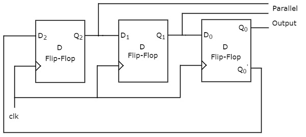
The 3-bit Johnson Ring counter also contains only a 3-bit SIPO shift register. The complemented output of rightmost D flip-flop is connected to serial input of left most D flip-flop.
Assume, initially all the D flip-flops are cleared. So, $\mathrm{Q_{2}Q_{1}Q_{0} \: = \: 000}$. Here, $\mathrm{Q_{2}}$ & $\mathrm{Q_{0}}$ are MSB & LSB respectively. We can understand the working of Johnson Ring counter from the following table.
| No of positive edge of Clock | Serial Input = Q0 | Q2(MSB) | Q1 | Q0(LSB) |
|---|---|---|---|---|
| 0 | - | 0 | 0 | 0 |
| 1 | 1 | 1 | 0 | 0 |
| 2 | 1 | 1 | 1 | 0 |
| 3 | 1 | 1 | 1 | 1 |
| 4 | 0 | 0 | 1 | 1 |
| 5 | 0 | 0 | 0 | 1 |
| 6 | 0 | 0 | 0 | 0 |
The initial status of the D flip-flops in the absence of clock signal is $\mathrm{Q_{2}Q_{1}Q_{0} \: = \: 000}$. This status repeats for every six positive edge transitions of clock signal.
Therefore, the following operations take place for every positive edge of clock signal.
Serial input of first D flip-flop gets the previous complemented output of third flip-flop. So, the present output of first D flip-flop is equal to the previous complemented output of third flip-flop.
The previous outputs of first and second D flip-flops are right shifted by one bit. That means, the present outputs of second and third D flip-flops are equal to the previous outputs of first and second D flip-flops.
Digital Electronics - Counters
Counter is a sequential circuit. A digital circuit which is used for a counting pulses is known counter. Counter is the widest application of flip-flops. It is a group of flip-flops with a clock signal applied. Counters are of two types.
- Asynchronous or Ripple Counters
- Synchronous Counters
Asynchronous or Ripple Counters
The logic diagram of a 2-bit ripple up counter is shown in figure. The toggle (T) flip-flop are being used. But we can use the JK flip-flop also with J and K connected permanently to logic 1. External clock is applied to the clock input of flip-flop A and QA output is applied to the clock input of the next flip-flop i.e. FF-B.
Logical Diagram

Operation
| Sr.No | Condition | Operation |
|---|---|---|
| 1 | Initially let both the FFs be in the reset state | QBQA = 00 initially |
| 2 | After 1st negative clock edge |
As soon as the first negative clock edge is applied, FF-A will toggle and QA will be equal to 1. QA is connected to clock input of FF-B. Since QA has changed from 0 to 1, it is treated as the positive clock edge by FF-B. There is no change in QB because FF-B is a negative edge triggered FF. QBQA = 01 after the first clock pulse. |
| 3 | After 2nd negative clock edge |
On the arrival of second negative clock edge, FF-A toggles again and QA = 0. The change in QA acts as a negative clock edge for FF-B. So it will also toggle, and QB will be 1. QBQA = 10 after the second clock pulse. |
| 4 | After 3rd negative clock edge |
On the arrival of 3rd negative clock edge, FF-A toggles again and QA become 1 from 0. Since this is a positive going change, FF-B does not respond to it and remains inactive. So QB does not change and continues to be equal to 1. QBQA = 11 after the third clock pulse. |
| 5 | After 4th negative clock edge |
On the arrival of 4th negative clock edge, FF-A toggles again and QA becomes 1 from 0. This negative change in QA acts as clock pulse for FF-B. Hence it toggles to change QB from 1 to 0. QBQA = 00 after the fourth clock pulse. |
Truth Table

Synchronous Counters
If the "clock" pulses are applied to all the flip-flops in a counter simultaneously, then such a counter is called as synchronous counter.
2-bit Synchronous Up Counter
The JA and KA inputs of FF-A are tied to logic 1. So FF-A will work as a toggle flip-flop. The JB and KB inputs are connected to QA.
Logical Diagram
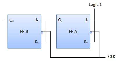
Operation
| Sr.No | Condition | Operation |
|---|---|---|
| 1 | Initially let both the FFs be in the reset state | QBQA = 00 initially. |
| 2 | After 1st negative clock edge |
As soon as the first negative clock edge is applied, FF-A will toggle and QA will change from 0 to 1. But at the instant of application of negative clock edge, QA , JB = KB = 0. Hence FF-B will not change its state. So QB will remain 0. QBQA = 01 after the first clock pulse. |
| 3 | After 2nd negative clock edge |
On the arrival of second negative clock edge, FF-A toggles again and QA changes from 1 to 0. But at this instant QA was 1. So JB = KB= 1 and FF-B will toggle. Hence QB changes from 0 to 1. QBQA = 10 after the second clock pulse. |
| 4 | After 3rd negative clock edge |
On application of the third falling clock edge, FF-A will toggle from 0 to 1 but there is no change of state for FF-B. QBQA = 11 after the third clock pulse. |
| 5 | After 4th negative clock edge |
On application of the next clock pulse, QA will change from 1 to 0 as QB will also change from 1 to 0. QBQA = 00 after the fourth clock pulse. |
Classification of Counters
Depending on the way in which the counting progresses, the synchronous or asynchronous counters are classified as follows −
- Up Counters
- Down Counters
- Up/Down Counters
UP/DOWN Counter
Up counter and down counter is combined together to obtain an UP/DOWN counter. A mode control (M) input is also provided to select either up or down mode. A combinational circuit is required to be designed and used between each pair of flip-flop in order to achieve the up/down operation.
Type of Up/Down Counters
There are two types of up/down counters −
- UP/DOWN Ripple Counters
- UP/DOWN Synchronous Counter
UP/DOWN Ripple Counters
In the UP/DOWN ripple counter all the FFs operate in the toggle mode. So either T flip-flops or JK flip-flops are to be used. The LSB flip-flop receives clock directly. But the clock to every other FF is obtained from (Q = Q bar) output of the previous FF.
- UP counting mode (M=0) − The Q output of the preceding FF is connected to the clock of the next stage if up counting is to be achieved. For this mode, the mode select input M is at logic 0 (M=0).
- DOWN counting mode (M=1) − If M = 1, then the Q bar output of the preceding FF is connected to the next FF. This will operate the counter in the counting mode.
Example
3-bit binary up/down ripple counter.
- 3-bit − hence three FFs are required.
- UP/DOWN − So a mode control input is essential.
- For a ripple up counter, the Q output of preceding FF is connected to the clock input of the next one.
- For a ripple up counter, the Q output of preceding FF is connected to the clock input of the next one.
- For a ripple down counter, the Q bar output of preceding FF is connected to the clock input of the next one.
- Let the selection of Q and Q bar output of the preceding FF be controlled by the mode control input M such that, If M = 0, UP counting. So connect Q to CLK. If M = 1, DOWN counting. So connect Q bar to CLK.
Block Diagram

Truth Table
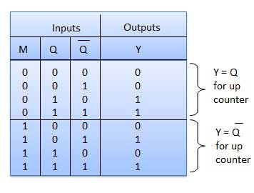
Operation
| Sr.No | Condition | Operation |
|---|---|---|
| 1 | Case 1 − With M = 0 (Up counting mode) |
If M = 0 and M bar = 1, then the AND gates 1 and 3 in fig. will be enabled whereas the AND gates 2 and 4 will be disabled. Hence QA gets connected to the clock input of FF-B and QB gets connected to the clock input of FF-C. These connections are same as those for the normal up counter. Thus with M = 0 the circuit work as an up counter. |
| 2 | Case 2 − With M = 1 (Down counting mode) |
If M = 1, then AND gates 2 and 4 in fig. are enabled whereas the AND gates 1 and 3 are disabled. Hence QA bar gets connected to the clock input of FF-B and QB bar gets connected to the clock input of FF-C. These connections will produce a down counter. Thus with M = 1 the circuit works as a down counter. |
Modulus Counter (MOD-N Counter)
The 2-bit ripple counter is called as MOD-4 counter and 3-bit ripple counter is called as MOD-8 counter. So in general, an n-bit ripple counter is called as modulo-N counter. Where, MOD number = 2n.
Type of Modulus
- 2-bit up or down (MOD-4)
- 3-bit up or down (MOD-8)
- 4-bit up or down (MOD-16)
Application of Counters
- Frequency counters
- Digital clock
- Time measurement
- A to D converter
- Frequency divider circuits
- Digital triangular wave generator.
Digital Electronics - Finite State Machines
Finite State Machines are the fundamental building blocks of various digital and computing systems. They provide a systematic approach to model the behavior of sequential circuits. They also help to control various processes in digital systems.
Read this chapter to learn the components, types, advantages, and applications of finite state machines.
What is a Finite State Machine?
A Finite State Machine (FSM) is a mathematical model that is used to explain and understand the behavior of a digital system. More specifically, it is a structured and systematic model that helps to understand the behavior of a sequential circuit that exists in a finite number of states at a given point of time.
In more simple words, a synchronous sequential circuit is also called as Finite State Machine FSM, if it has a finite number of states.
The transition of these finite states takes place based on the internal or external inputs that results in the predictable and systematic changes in the behavior of the system.
Components of a Finite State Machine
A typical finite state machine consists of the following main components −
Finite States
The finite states are nothing but the distinct modes or conditions in the given system. Each of these finite states represents a specific behavior. In digital system representation, these finite states are generally represented through symbols or labels.
State Transitions
In terms of finite state machines, the state transition can be defined as the change from one state to another. This change in state or state transition takes placed based on some specific inputs or conditions. These state transitions are generally triggered by events which are associated with some rules or conditions and determine the next state of the system.
State Diagram
The state transition and the behavior of a finite state machine can be represented in a graphical form that is known as state diagram of the finite state machine.
Inputs
The inputs to the finite state machines are the external signals that trigger the state transitions in the system. These inputs are to be entered into the finite state machine by using sensors, user input devices like mic, keyboard, etc.
Outputs
The results produced by the system as per the inputs and current states are known as outputs. These outputs of the system can be used to trigger events, control actuators, or to provide feedback to the external environment.
Types of Finite State Machine
There are two types of finite state machines namely,
- Mealy State Machine
- Moore State Machine
Let us now discuss these two types of finite state machines in detail.
Mealy State Machine
A Finite State Machine is said to be a Mealy state machine, if its outputs depend on both present inputs & present states. The block diagram of the Mealy state machine is shown in the following figure −
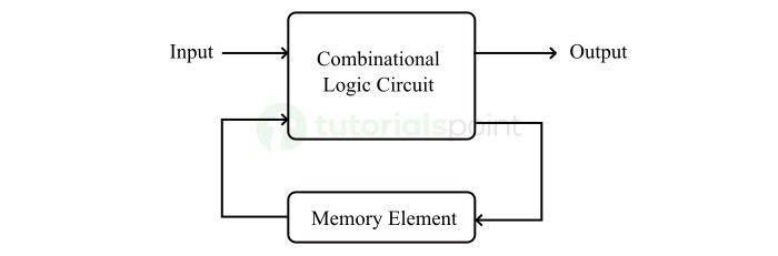
As shown in the figure, there are two main parts presents in the Mealy state machine. Those are combinational logic circuit and memory element. The memory element is useful to provide some part of previous outputs and present states as inputs to the combinational logic circuit.
Based on the present inputs and present states, the Mealy state machine produces outputs. Therefore, the outputs will be valid only at positive or negative transition of the clock signal.
State Diagram of Mealy State Machine
The state diagram of Mealy state machine is shown in the following figure.

In the above figure, there are three states, namely A, B and C. These states are labelled inside the circles and each circle corresponds to one state. State transitions between these states are represented with directed lines. Here, 0 / 0, 1 / 0 and 1 / 1 denote the input / output. In the above figure, there are two state transitions from each state based on the value of input.
In general, the number of states required in Mealy state machine is less than or equal to the number of states required in Moore state machine. There is an equivalent Moore state machine for each Mealy state machine.
Moore State Machine
A Finite State Machine is said to be a Moore state machine, if its outputs depend only on the present states.
The block diagram of the Moore state machine is shown in the following figure −
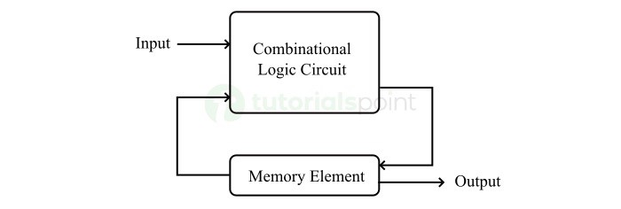
As shown in above figure, there are two parts presents in a Moore state machine. Those are combinational logic and memory. In this case, the present inputs and present states determine the next states. So, based on next states, Moore state machine produces the outputs. Therefore, the outputs will be valid only after transition of the state.
State Diagram of Moore State Machine
The state diagram of Moore state machine is shown in the following figure −
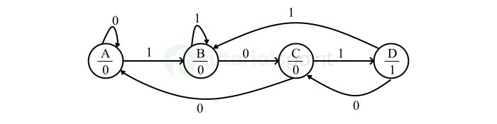
In the above figure, there are four states, namely A, B, C, and D. These states and the respective outputs are labelled inside the circles. Here, only the input value is labeled on each transition. In the above figure, there are two transitions from each state based on the value of input.
In general, the number of states required in Moore state machine is more than or equal to the number of states required in Mealy state machine. There is an equivalent Mealy state machine for each Moore state machine. So, based on the requirement we can use one of them.
Advantages of Finite State Machine
The Finite State Machines have several advantages in the field of digital electronics. All these advantages make them a crucial tool for modeling and implementing various digital systems. Some key advantages of Finite State Machines are listed below −
- Finite state machines provide a simple and systematic way to model and understand the behavior of digital systems with discrete finite states and transitions between them.
- Finite state machines support modular designs that help to breakdown the complex digital systems into smaller components. Each component of the finite state machine can represent a specific task of the entire system. This allows for easier design, testing, and maintenance.
- Finite state machines provide ease in terms of scalability that allows for addition of new states and transitions, and logics to the existing system without altering its fundamental structure or operation. This becomes essential when the system requirement evolve or expand.
- Fundamentally, finite state machines have a deterministic or predictable behavior. That means, we can easily determine the next state of the system from its current state and the inputs. This predictable behavior helps us to ensure the reliable and consistent operation of the system. It also makes the finite state machines best suited for real-time and safety-critical applications.
- Finite state machines are considered highly efficient in terms of both hardware and software implementations, as they require minimal hardware and software resources such as logic gates, memory, and other processing resources.
- Finite state machines support parallelism. This technology allows the occurrence of multiple states and state transitions simultaneously within the system. It also optimizes the performance and improves the responsiveness of the system.
- Finite state machines are versatile tools in the field of digital electronics and computer science, as they find their applications in various fields such as digital system design, control system design, software development, development of artificial intelligence, etc.
Applications of Finite State Machine
In the field of digital electronics and computer science, the finite state machines are used in various applications due to their ability to model sequential logic systems effectively. Here are some examples of applications of finite state machines −
- Finite state machines are commonly used in designing and implementation of different types of sequential logic circuits, such as digital counters, timers, control units, etc.
- Finite state machines are used in digital control systems to control and regulate the behavior of complex automated systems, like robots, industrial control and automation systems, etc.
- Finite state machines are used in the implementation of communication protocols like network protocols and state-based digital systems like data transmission and protocol converters.
- Finite state machines are also used in the field of software development to model and define the behavior of state-based systems in applications, to create user interfaces, to implement game mechanics, and to develop workflow management systems.
Conclusion
In conclusion, finite state machines are important and powerful tools used in the field of digital electronics to model, design, and analyze the behavior of state-based digital systems and synchronous sequential circuits.
Finite state machines allow engineers and system designers to design and implement efficient, reliable, and scalable systems that can handle complex state-based logics and processes in the field of digital electronics and computer engineering.
Algorithmic State Machine
Every digital system can be partitioned into two parts. Those are data path (digital) circuits and control circuits. Data path circuits perform the functions such as storing of binary information (data) and transfer of data from one system to the other system. Whereas, control circuits determine the flow of operations of digital circuits.
It is difficult to describe the behavior of large state machines using state diagrams. To overcome this difficulty, Algorithmic State Machine (ASM) charts can be used. ASM charts are similar to flow charts. They are used to represent the flow of tasks to be performed by data path circuits and control circuits.
Basic Components of ASM charts
Following are the three basic components of ASM charts.
- State Box
- Decision Box
- Conditional Output Box
State Box
State box is represented in rectangular shape. Each state box represents one state of the sequential circuit. The symbol of state box is shown in the following figure.

It is having one entry point and one exit point. Name of the state is placed to the left of state box. The unconditional outputs corresponding to that state can be placed inside state box. Moore state machine outputs can also be placed inside state box.
Decision Box
Decision box is represented in diamond shape. The symbol of decision box is shown in the following figure.

It is having one entry point and two exit paths. The inputs or Boolean expressions can be placed inside the decision box, which are to be checked whether they are true or false. If the condition is true, then it will prefer path1. Otherwise, it will prefer path2.
Conditional Output Box
Conditional output box is represented in oval shape. The symbol of conditional output box is shown in the following figure.
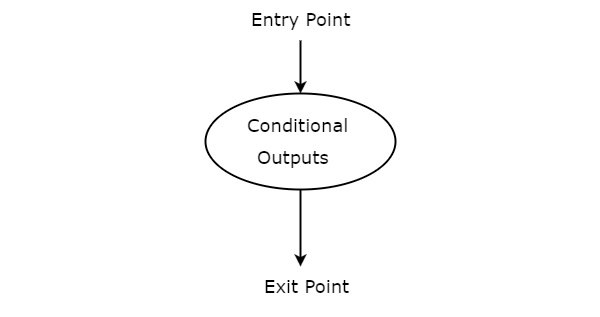
It is also having one entry point and one exit point similar to state box. The conditional outputs can be placed inside state box. In general, Mealy state machine outputs are represented inside conditional output box. So, based on the requirement, we can use the above components properly for drawing ASM charts.
Analog to Digital Converter
An analog-to-digital converter, also known as ADC, is a digital circuit used to convert analog signals into digital format.
The conversion of analog signals into digital format is crucial for their processing with the help of digital systems like microprocessors, microcontrollers, digital signal processors (DSPs), etc. Therefore, ADCs are important components in several digital systems like computers and other digital devices.
In this chapter, we will explain in detail the concept, components, types, and applications of analog to digital converters.
What is an Analog to Digital Converter?
An analog to digital converter is a digital circuit designed to perform conversion of analog signals into digital data format. It is also known ADC. Analog to digital converters are essential components in digital systems like computers, data processors, digital communication systems, etc.
The following figure depicts the block diagram of an analog to digital converter −
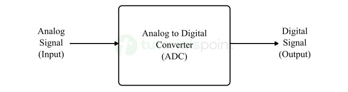
From this figure, it is clear that the input to an analog to digital converter is an analog or natural signal and the output is a digital or discrete time signal.
In practical systems, the analog to digital converter serves as an interface between external environment and a digital system.
Working of Analog to Digital Converter
The working of an analog to digital converter involves the processes explained below −
Inputting Analog Signal
An analog to digital converter takes an analog signal as input. The analog signal could be a voltage, current, temperature, pressure, or any other physical quantity that changes continuously with time.
Sampling
At this stage, the analog to digital converter samples the input analog signal at regular intervals of time. These time intervals are defined in terms of sampling rate.
In the sampling process, the analog signal that varies continuously over time is measured at discrete instants of time to collect discrete values of the signal.
Quantization
Quantization is a process of assigning a digital or discrete value to each sampled value of the analog signal. In the process of quantization, the range of all possible analog values is divided into a finite number of discrete digital values.
Encoding
Encoding is a process of converting the quantized digital values into their equivalent binary numbers. These encoded binary numbers represent the sampled analog values in the digital format.
The resolution, accuracy, and precision of the analog to digital converter is determined by the number of bits used for encoding.
Outputting Digital Signal
At the end, the analog to digital converter produces a digital signal as output. This output digital signal can be processed, stored, or transmitted by digital systems.
Performance Factors of Analog to Digital Converters
The performance of an analog to digital converter can be evaluated using several different factors. The following two are the most important −
Signal-to-Noise Ratio (SNR) of ADC
The Signal-to-Noise Ratio (SNR) of an analog to digital converter is defined as the measure of ability of the converter to differentiate between the desired signal and unwanted noise signal.
Mathematically, the SNR of an analog to digital converter is expressed as the ratio of the power of the electrical signal (that represents the useful information) to the power of the noise signal (that represents the unwanted disturbances).
In practice, the SNR is expressed in decibels (dB) and the formula for calculating the SNR of an ADC is given below,
$$\mathrm{SNR \: of \: ADC \: = \: 10 \: \times \: log ( \frac{Electrical \: Signal \: Power}{Noise \: Signal \: Power})}$$
From this expression, it is clear that a higher SNR represents better performance of the analog to digital converter. In other words, an analog to digital converter having a high SNR distinguishes the electrical signal from the noise signal more clearly. Therefore, it is desirable that the analog to digital converter have a high SNR so that it can accurately capture and digitalize smaller analog signals even in the presence of noise signals.
Bandwidth of Analog to Digital Converter
The bandwidth of an analog to digital converter is nothing but the range of frequencies that it can sample and digitalize accurately. The sampling rate of the analog to digital converter determines its bandwidth. Where, the sampling rate is defined as the number of samples of the analog signal taken per second.
According to the Nyquist-Shannon sampling theorem, the maximum sampling rate of an analog to digital converter should be at least double of the maximum frequency component present in the input analog signal. It is an important factor to avoid misidentification of the signal that can introduce distortion or error in sampling.
Let us take an example to understand this, consider an analog to digital converter having a maximum sampling rate of 150 kHz, then its bandwidth should be limited to frequencies less than 75 kHz to prevent distortion.
Hence, it is important that the analog to digital converter should have a sufficient bandwidth to capture the high-frequency analog signals accurately.
Types of Analog-to-Digital Converters
In digital electronics, different types of analog-to-digital converters (ADCs) are designed to fulfil the requirements of different applications.Some of common types of analog-to-digital converters include the following −
- Flash ADC
- Semi-Flash ADC
- Successive Approximation Register ADC
- Sigma-Delta ADC
- Pipelined ADC
Flash ADC
Flash ADC, also known as Direct ADC, is the fastest ADC available. This type of ADC has sampling rates of the order of gigahertz. The flash ADCs offer such high speeds because they use a bank of comparators that can operate in parallel, each for a certain voltage range.
However, the flash ADCs are relatively larger in size and costlier than other types of ADCs. Also, they consume relatively more power. In the case of a flash ADC, if "n bits" is resolution of the ADC, then it requires (2n 1) comparators in its bank. For example, a flash ADC having 8-bit resolution requires (28 1 = 255) comparators.
The flash analog-to-digital converters are mainly used in digitization of video signals or fast signals in optical storage.
Semi-Flash ADC
The Semi-Flash ADC is a type of analog-to-digital converter that combines the fast speed of a flash ADC with a reduced number of comparators. These two features together make the semi-flash ADC compact in size and cost effective as compared to a flash ADC.
In a semi-flash analog to digital converter, two separate flash converters are used that operate in parallel. Each converter has a resolution that is half the number of bits of the whole semi-flash ADC. One converter handles the most significant bits (MSBs) and the other converter handles the least significant bits (LSBs) of the signal.
After processing, the outputs produced by the two converters are combined to generate the final digital output of the semi-flash ADC.
The most significant advantage of the semi-flash analog to digital converter is that it requires a lesser number of comparators than an ordinary flash ADC with maintaining the high-speed operation. This results in smaller size, reduced complexity and cost. However, it takes more time to complete the conversion process because it requires some additional time to combine the partial results of the two separate converters.
The semi-flash analog-to-digital converters are widely used in applications that require a balance between speed, resolution, and cost.
Successive Approximation Register ADC
The Successive Approximation Register Analog to Digital Converter, abbreviated as SAR ADC, is a type of analog to digital converter that uses a series of comparisons to determine each bit of the digital output.
The SAR ADC starts working by initializing its internal approximation registers. Then, it takes a sample of the input analog signal and stores it steady until the conversion process completes.
After that a binary search algorithm is utilized to perform approximation of the input signal. This process starts by setting the most significant bit (MSB) of the output digital signal to the highest value and compares this value with the sampled input analog signal.
In the next step, the SAR ADC compares the sampled input analog signal with the output of an internal digital-to-analog converter that produces a signal proportional to the current approximation of the input signal.
Depending on results of the comparison, the SAR ADC successively changes the value of each bit in the digital output until the desired output is obtained. Once all bits of the digital output have been determined, the SAR converter completes the conversion process. The digital output obtained represents the digital approximation of the sampled input analog signal.
The SAR analog-to-digital converters are commonly used in various applications, such as consumer electronics, medical instruments, data acquisition systems, etc.
Sigma-Delta ADC
The Sigma-Delta Analog-to-Digital Converter, also represented as ADC, is a type of analog to digital converter that provides a high resolution and is used in applications that require precise measurement and signal processing like in audio recording, high-quality audio systems, sensor-based systems, precise instruments, etc.
The working of a sigma-delta ADC involves the following processes −
First, it samples the analog input signal at a frequency significantly higher than the Nyquist rate to capture more information about the input signal. This process is called oversampling.
Then, delta modulation is used to convert the oversampled analog signal into a series of digital pulses. In the process of delta modulation, the difference or delta between successive samples of the analog input signal is quantized and converted into digital form.
Now, the sigma-delta modulation is performed, in which a sigma-delta modulator is used to modulate the difference between the actual analog signal and its digital form. In this modulation, the quantization noise is pushed away from the desired frequency band and towards the higher frequencies.
After sigma-delta modulation, the digital signal is passed through a low-pass filter that removes the high-frequency noise that can be introduced during oversampling and sigma-delta modulation. This low-pass filter produces a high-resolution digital output by extracting the low-frequency components.
At the end of the conversion process, the digital signal is down-sampled (i.e., decimated) to decrease its sample rate to the desired output rate.
Pipelined ADC
The Pipelined Analog to Digital Converter is a type of ADC which is similar to the SAR ADC, but it performs a coarse and refined conversion. It provides a balance between resolution and speed that make it suitable to use in communication systems, medical test equipment, multimedia, industrial control systems, etc.
A pipelined ADC works in multiple stages, where each stage completes a specific part of the analog-to-digital conversion. It is called pipelined ADC because all stages take place in a pipeline manner, in which the output of one stage enters into the next stage.
In the pipelined ADC, the analog input signal is divided into multiple subranges and each stage of the pipeline performs quantization of a subrange to convert the analog input signal into digital form. It is important to note that all stages of the pipelined ADC operate in parallel to provide a faster conversion rate.
The pipelined ADC uses various digital correction techniques such as digital calibration, error correction algorithms, and digital filtering to remove errors that can be introduced during the analog-to-digital conversion process. This improves the accuracy and reliability of the digital output.
This is all about some commonly used types of analog to digital converters (ADCs) in digital electronics.
Applications of Analog to Digital Converter
Analog-to-digital converters (ADCs) are used in various industries and fields where analog signals have to be processed, analyzed, or transmitted using digital systems like computers. Some common applications of analog to digital converters are listed below −
- In the field of digital signal processing, ADCs are used for converting analog signals obtained from sensors, microphones, or other analog devices into digital format for processing them using digital processors.
- In audio processing applications, ADCs are used to convert analog audio signals into digital format for storage, manipulation, and transmission in digital systems.
- ADCs are essential components in various data acquisition systems used in the field of scientific research, industrial automation, and instrumentation.
- In communication systems, ADCs are used to convert analog audio or video signals into digital format for transmission over communication channels.
- ADCs are used in radio receivers for digitization of received radio frequency (RF) signals.
- ADCs play an important role in several medical equipment and healthcare systems for converting various analog bio-signals and physiological parameters like heart rate, blood pressure, oxygen saturation, EEG signals, etc. into digital format to process them using digital systems.
- In automotive electronics, ADCs are used to convert analog signals received from sensors measuring parameters such as temperature, torque, speed, etc. into digital format for driver assistance and vehicle diagnostics.
- ADCs are also used in a wide range of consumer electronic devices such as smartphones, tablets, laptops, entertainment equipment, etc.
These are a few examples of the applications of analog-to-digital converters (ADCs) in various fields and industries.
Conclusion
In this chapter, we explained in detail about analog to digital converters, their types and applications. In conclusion, an analog to digital converter is an electronic circuit that can convert an analog input signal into a digital output signal.
ADCs are important components in several devices and systems used across various industries. This is because, the signals received in real-time like voice signals, signals from sensors, etc. are analog in nature and they cannot be processed using digital systems like computers. ADCs help to overcome this interfacing issue. Basically, ADCs act as an interface between an analog input device and a digital processing element.
Digital to Analog Converter
A Digital to Analog Converter (DAC) converts a digital input signal into an analog output signal. The digital signal is represented with a binary code, which is a combination of bits 0 and 1 while the analog signal is a continuous time function.
This chapter deals with Digital to Analog Converters in detail. The block diagram of DAC is shown in the following figure −
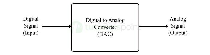
A Digital to Analog Converter (DAC) consists of a number of binary inputs and a single output. In general, the number of binary inputs of a DAC will be a power of two.
Types of Digital to Analog Converters
Depending on the construction and structure, there are two types of digital to analog converters, they are −
- Weighted Resistor DAC
- R-2R Ladder DAC
The following sections discuss about these two types of DACs in detail.
Weighted Resistor DAC
A weighted resistor DAC produces an analog output, which is almost equal to the digital (binary) input by using binary weighted resistors in the inverting adder circuit. In short, a binary weighted resistor DAC is called as weighted resistor DAC.
The circuit diagram of a 3-bit binary weighted resistor DAC is shown in the following figure −
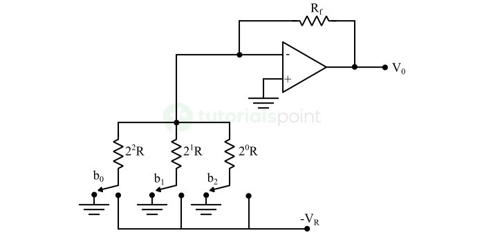
Recall that the bits of a binary number can have only one of the two values. i.e., either 0 or 1. Let the 3-bit binary input is b2b1b0. Here, the bits b2 and b0 denote the Most Significant Bit (MSB) and Least Significant Bit (LSB) respectively.
The digital switches shown in the above figure will be connected to ground, when the corresponding input bits are equal to '0'. Similarly, the digital switches shown in the above figure will be connected to the negative reference voltage, VR when the corresponding input bits are equal to '1'.
In the above circuit, the non-inverting input terminal of an op-amp is connected to ground. That means zero volts is applied at the non-inverting input terminal of op-amp.
According to the virtual short concept, the voltage at the inverting input terminal of op-amp is same as that of the voltage present at its non-inverting input terminal. So, the voltage at the inverting input terminals node will be zero volts.
The nodal equation at the inverting input terminals node is −
$$\mathrm{\frac{0 \: + \: V_{R}b_{2}}{2^{0}R} \: + \: \frac{0 \: + \: V_{R}b_{1}}{2^{1}R} \: + \: \frac{0 \: + \: V_{R}b_{0}}{2^{2}R} \: + \: \frac{0 \: - \: V_{0}}{R_{f}} \: = \: 0}$$
$$\mathrm{\Rightarrow \: \frac{V_{0}}{R_{f}} \: = \: \frac{V_{R}b_{2}}{2^{0}R} \: + \: \frac{V_{R}b_{1}}{2^{1}R} \: + \: \frac{V_{R}b_{0}}{2^{2}R}}$$
$$\mathrm{\Rightarrow \: V_{0} \: = \: \frac{V_{R}R_{f}}{R}(\frac{b_{2}}{2^{0}} \: + \: \frac{b_{1}}{2^{1}} \: + \: \frac{b_{0}}{2^{2}})}$$
Substituting, R = 2Rf in the above equation,
$$\mathrm{V_{0} \: = \: \frac{V_{R}R_{f}}{2R_{f}}(\frac{b_{2}}{2^{0}} \: + \: \frac{b_{1}}{2^{1}} \: + \: \frac{b_{0}}{2^{2}})}$$
$$\mathrm{\therefore \: V_{0} \: = \: \frac{V_{R}}{2}(\frac{b_{2}}{2^{0}} \: + \: \frac{b_{1}}{2^{1}} \: + \: \frac{b_{0}}{2^{2}})}$$
The above equation represents the output voltage equation of a 3-bit binary weighted resistor DAC. Since the number of bits are three in the binary (digital) input, we will get seven possible values of output voltage by varying the binary input from 000 to 111 for a fixed reference voltage, VR.
We can write the generalized output voltage equation of an N-bit binary weighted resistor DAC as shown below based on the output voltage equation of a 3-bit binary weighted resistor DAC.
$$\mathrm{\therefore \: V_{0} \: = \: \frac{V_{R}}{2}(\frac{b_{N-1}}{2^{0}} \: + \: \frac{b_{N-2}}{2^{1}} \: + \dotso \: + \: \frac{b_{0}}{2^{N-1}})}$$
Disadvantages of Weighted Resistor DAC
The disadvantages of the binary weighted resistor DAC are as follows −
- The difference between the resistance values corresponding to LSB & MSB will increase as the number of bits present in the digital input increases.
- It is difficult to design more accurate resistors as the number of bits present in the digital input increases.
R-2R Ladder DAC
The R-2R Ladder DAC overcomes the disadvantages of a binary weighted resistor DAC. As the name suggests, R-2R Ladder DAC produces an analog output, which is almost equal to the digital (binary) input by using a R-2R ladder network in the inverting adder circuit.
The circuit diagram of a 3-bit R-2R Ladder DAC is shown in the following figure −
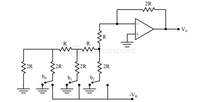
Recall that the bits of a binary number can have only one of the two values. i.e., either 0 or 1. Let the 3-bit binary input is b2b1b0. Here, the bits b2 and b0 denote the Most Significant Bit (MSB) and Least Significant Bit (LSB) respectively.
The digital switches shown in the above figure will be connected to ground, when the corresponding input bits are equal to '0'. Similarly, the digital switches shown in above figure will be connected to the negative reference voltage, VR when the corresponding input bits are equal to '1'.
It is difficult to get the generalized output voltage equation of a R-2R Ladder DAC. But we can find the analog output voltage values of R-2R Ladder DAC for individual binary input combinations easily.
Advantages of R-2R Ladder DAC
The advantages of a R-2R Ladder DAC are as follows −
- R-2R Ladder DAC contains only two values of resistor: R and 2R. So, it is easy to select and design more accurate resistors.
- If a greater number of bits are present in the digital input, then we have to include required number of R-2R sections additionally.
Due to the above advantages, R-2R Ladder DAC is preferable over binary weighted resistor DAC.
Important Parameters of DACs
The following are some key parameters and factors that we must consider while selecting a digital to analog converter for a specific application −
Resolution
The number of discrete output levels that a digital to analog converter can produce is known as its resolution. To obtain a smoother and accurate analog output signal, the resolution of the digital to analog converter must be significantly high. The resolution of a DAC is typically measured in bits.
Let us understand the importance of resolution of DAC. Consider a DAC that can handle 8-bits, it can represent 28 = 256 discrete output values. On the other hand, if a DAC can handle 16-bits, then it is able to represent 216 = 65536 discrete output values. Hence, the DAC with 16-bits can provide a smoother and more accurate representation of the digital signal in analog format as compared to that the 8-bit DAC can do.
Accuracy
The accuracy of a digital to analog converter is the measure of how closer is the output analog signal to the input digital signal. The high accuracy of DAC is an essential factor to produce a highly precise analog output signal.
Power Consumption
This factor provides information about the power consumed by the digital to analog converter during its operation. Ideally, a digital to analog converter must be power efficient, so that it can extend the battery life and minimize the operational cost.
Operating Speed
The operating speed of a digital to analog converter represents the rate at which the DAC converts a digital signal into analog signal. Typically, the speed of a DAC is measured in samples per second (S/s) or megahertz (MHz).
The operating speed of the digital to analog converter also determines the maximum frequency of the analog output signal that the DAC can generate accurately.
It is essential that a digital to analog converter used in applications like real-time signal processing, generation of fast waveforms, high-speed communication, etc. must have a significantly high-speed.
Noise Performance
The noise performance of a digital to analog converter represents the amount of noise that can be introduced in the output signal during the conversion process. The unwanted noise can affect the signal-to-noise ratio and hence the signal quality. Therefore, we should minimize the noise as much as possible to obtain a high-quality output analog signal.
Applications of Digital to Analog Converters
Digital to analog converters are widely used in a variety of applications in the field of digital electronics. The main function of a digital to analog converter is to convert a digital signal into analog format.
The following are some common devices and systems in which the digital to analog converters are used −
- Audio amplifiers and playback systems
- Video encoder systems
- Data acquisition systems
- Calibration of testing and measuring instruments
- Motor control circuits
- Digital signal processors
- Telecommunication systems, etc.
Conclusion
Digital to analog converters are used in the field of electronics to provide an interface between digital input and analog output. In this chapter, we explained in detail about the types and applications of analog to digital converters.
DAC and ADC ICs
A digital to analog converter is an electronic device that converters a digital signal into analog format. On the other hand, an analog to digital converter is an electronic device that converters an analog signal into digital format. Both DAC (Digital to Analog Converter) and ADC (Analog to Digital Converter) play an important role in different fields of electronic such as communication, signal processing, computing technologies, control and automation systems, and more.
With the advancement of technology, we can design and implement the analog to digital converters and digital to analog converters in the form of IC or integrated circuits. This chapter is meant for explaining some important ADC and DAC ICs commonly used in electronic circuits and systems.
What are DAC and ADC ICs?
DAC and ADC ICs are small electronic devices and integrated circuits used in the field of electronics to convert a digital signal into analog format and analog signal into digital format respectively.
The ADC IC (Analog to Digital Converter IC) is used to convert analog signals into digital format. These ICs take the analog signals as input and sample them at regular intervals of time. Then, they produce digital representation of the analog input signal as output.
There is another type of IC called DAC IC (Digital to Analog Converter IC) that is used to convert digital signals into analog format. Hence, the DAC ICs take digital signals as input and produce their analog representation as output.
The ADC and DAC ICs are important components in several different types of electronic systems where converting signals between the analog and digital formats are crucial.
Popular DAC and ADC ICs
The following are some commonly used DAC and ADC ICs that are widely used in various electronic applications −
- ADC 0809 (8-Bit ADC IC)
- ICL 7109 (12-Bit Binary ADC IC)
- DAC 0808 (8-Bit DAC IC)
Let us discuss about these ADC and DAC ICs in detail along with their features and applications.
ADC 0809 IC
The ADC 0809 IC is an analog to digital converter IC. It is a monolithic CMOS device that consists of an 8-bit analog to digital converter, an 8-bit multiplexer, and a microprocess compatible control unit.
The ADC 0809 IC uses successive approximation technique to perform analog to digital conversion. It comes in a 28-pin molded IC carrier package. The pin diagram of the ADC 0809 IC is shown in the following figure.

This IC is one of the widely used ADC ICs in various digital electronics and microcontroller-based circuits and systems to convert analog signals into their digital format.
Features of ADC 0809 IC
Some of the key features of ADC 0809 IC are listed below −
- The ADC 0809 IC is an 8-bit analog to digital converter IC. Hence, it can represent an analog input signal with a resolution of 8 bits or 28 = 256 possible discrete values in digital format.
- The ADC 0809 IC provides an easy interfacing with all microprocessors.
- It does not require the external zero or full-scale adjustments.
- It also consists an 8-channel single ended analog signal multiplexer.
- It can operate ratiometrically or with a 5 V DC voltage or an analog span adjusted voltage reference.
- The output of the ADC 0809 IC meets the TTL voltage level requirements.
- The ADC 0809 IC can operate with low power consumption, typically 15 mW that makes making it best suited for batterypowered devices.
- It can support 0 V to 5V input analog voltage range with a single supply of 5 V DC.
- It has a conversion time of around 100 s.
Applications of ADC 0809 IC
The ADC 0809 IC is an ideal device in various applications such as automation, process and machine control, consumer electronics, automotives, etc. Some common applications of this ADC IC are listed here −
- The ADC 0809 IC is most commonly used in data acquisition systems to convert analog input signals received from sensors, transducers, and other analog measuring devices into digital format to process and analyze them using digital systems.
- The ADC 0809 IC is also used in different applications in the field of instrumentation and control engineering. It is mainly employed for precise measurement and monitoring of analog signals like temperature, pressure, and motor control.
- In the field of industrial automation, the ADC 0809 IC is used for digitalization of analog process and control signals which are then used for automation and monitoring of control and manufacturing processes.
- The ADC 0809 IC is also used in various consumer electronic devices such as digital multimeters, audio and music systems, etc. for providing an interface between analog signals and digital circuits.
ICL 7109 IC
The ICL 7109 IC is a monolithic 12-Bit analog to digital converter (ADC) IC primarily designed for easy interfacing with microprocessor-based systems and Universal Asynchronous Receiver-Transmitter (UART).
The ICL 7109 IC comes in a 40-pin IC package whose pin configuration diagram is shown in the following figure −
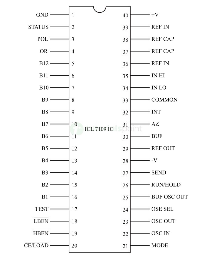
Features of ICL 7109 IC
Some of the key features of the ICL 7109 ADC IC are described below −
- The ICL 7109 IC is a 12-bit dual slope integrating analog to digital converter IC. Hence, it provides a resolution of 12-bits that enables it to represent the analog input signals with a higher precision in digital format.
- The ICL 7109 IC provides an easy interfacing with microprocessors. This feature makes it ideally suitable for applications where analog signals are required to be processed or analyzed using digital systems like computers.
- The ICL 7109 IC also provides facility of interfacing with UART (Universal Asynchronous Receiver/Transmitter) systems. This feature allows for serial data transmission and communication with external digital devices. It also has some control lines like RUN/(HOLD) inputs and STATUS output that can be used to monitor and control the conversion timing.
- The ICL 7109 IC does not require any special handling precautions because its all inputs are fully protected against static discharge.
- The ICL 7109 IC provides true differential input and differential reference. It provides low noise and high accuracy.
- The ICL 7109 IC offers a low drift typically less than 1 V/C. This ensures high precision in analog to digital conversion under varying environmental conditions.
- The ICL 7109 IC consumes les power that makes it ideally suitable for battery powered devices.
Applications of ICL 7109 IC
The ICL 7109 IC is one of the commonly used analog to digital converter IC in various digital and microprocessor based systems. Here are some common examples of applications of the ICL 7109 IC −
- The ICL 7109 IC is commonly used in digital systems where accurate and high-performance conversion of analog signals into digital format is needed. It widely used in industrial monitoring, instrumentation, and scientific measurement systems.
- Since the ICL 7109 IC is compatible with Universal Asynchronous Receiver/Transmitter (UART) systems. Hence, it is used for interfacing between industry standard UARTs for transmission of digital data serially over communication channels.
- In industrial automation and control systems, the ICL 7109 IC is employed for converting analog process and control signals into digital data for processing and controlling by microprocessors and microcontrollers.
- Due to high accuracy and low power consumption, the ICL 7109 IC is best suited to utilize in battery powered testing and measuring instruments, where precise measurement of analog signals is desired.
- The ICL 7109 IC is also used in numerous consumer electronic devices for converting analog signals into digital format accurately, which is crucial for proper functioning of the device.
DAC 0808 IC
The DAC 0808 IC is an 8-bit digital to analog converter IC designed to convert a digital input signal into its analog representation. It is a monolithic IC known for its high accuracy and low power consumption in digital to analog conversion process.
This IC comes in the dual-in-line IC package with 16 pins. The following depicts the pin diagram of the DAC 0808 IC.
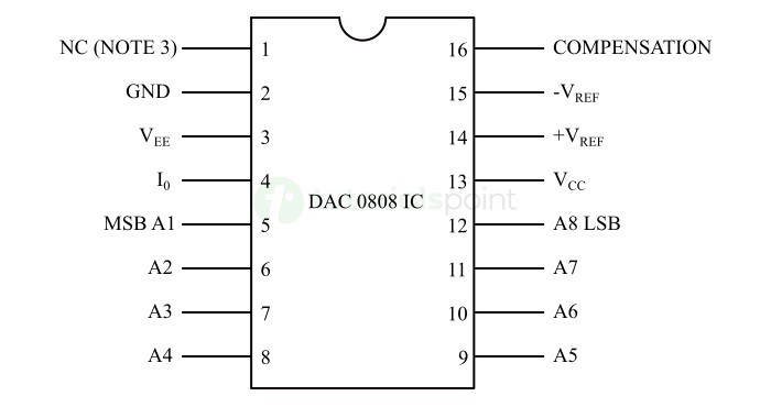
Due to its features like high accuracy, low power consumption, and fast settling time, it is commonly used in microcontroller-based and other digital electronic systems.
Features of DAC 0808 IC
The following are the key features of DAC 0808 IC, making it best suited to use in digital systems −
- The DAC 0808 IC has a resolution of 8-bits. Hence, it can convert a digital input signal into the analog format precisely. It provides high accuracy in digital to analog conversion. Typically, it can convert a digital signal into analog format with a maximum error of around $\mathrm{\pm 0.9 \%}$.
- The DAC 0808 IC produces a full-scale current match, typically $\mathrm{\pm 1}$ LSB. This feature helps maintain the relative accuracy in the output current.
- The DAC 0808 IC has a fast-settling time typically 150 ns. Thus, this IC can adjust its output to match the desired analog voltage in a very short time.
- The DAC 0808 IC is compatible with both TTL and CMOS devices.
- The DAC 0808 IC has a high-speed multiplying input slew rate. Therefore, it can change its output voltage at a very fast speed when the digital input to it changes. Typically, the slew rate of the DAC 0808 IC is 8 mA/s.
- The DAC 0808 IC can operate with a power supply voltage range varying from $\mathrm{\pm 4.5}$ V to $\mathrm{\pm 18}$ V. This feature makes it versatile to use in systems operating at different voltage levels.
- The DAC 0808 IC consumes very low power. Typically, it consumes only 33 mW of power at an operating voltage of $\mathrm{\pm 5}$ V. This feature makes it suitable to use in battery power devices where energy efficiency is critical.
Applications of DAC 0808 IC
The DAC 0808 IC is widely used in a variety of applications across different fields such as audio signal processing, industrial automation, and control systems for the conversion of digital signals into analog voltages. Some key examples illustrating the applications of the DAC 0808 IC are given below −
- The DAC 0808 IC is very commonly used in waveform generators to produce analog output voltages from digital input data. It allows us to produce various types of waveforms like sine waves, square waves, triangular waves, etc.
- In the field of instrumentation and control, the DAC 0808 IC is employed for producing analog signals that can be used in calibration, simulation, and testing applications.
- The DAC 0808 IC is also used in motor control circuits to produce analog voltage signals from digital inputs. These analog output signals are then used for operating motor drives, actuators, and servo systems.
- The DAC 0808 IC is also used in various audio systems such as audio playback systems, synthesizers, musical instruments, audio effects processors, etc. to perform digital to analog conversion.
- In industrial automation and control systems, the DAC 0808 IC is utilized to produce analog signals used to control and regulate the processes, operate the valves, and adjust the system variables based on digital inputs provided by microcontrollers or PLCs.
Conclusion
There are several different ADC and DAC ICs available in the market and are used depending on the specific requirements of the application. In this chapter, we explained the pin diagram, key features, and applications of some popular types of DAC and ADC ICs.
In conclusion, a DAC IC is a digital to analog converter chip that can convert digital input signals into analog output voltages at a very high speed and efficiency. On the other hand, an ADC IC is an analog to digital converter chip that converts analog input signals into digital output signals. These ICs are so designed that they are compatible with various digital systems and low power devices.
Implementation of NOT Gate using NAND Gate
Before getting into implementing a NOT gate using NAND gate, lets have a basic overview of NOT gates and NAND gates.
What is NOT Gate?
NOT gate is a basic logic gate used in digital electronic circuits. The NOT gate has a single input and a single output. The output of the NOT gate is the logical inversion of its input. For this reason, the NOT gate is also known as inverter.

The symbol of the standard NOT gate has a triangle pointing to the right with a circle at its right end as shown in figure-1. This circle is referred to as an inversion bubble. The NOT gate produces an output which is the complement or inversion of its input. For example, if we give a HIGH input single, then it provides a LOW output signal. Similarly, when we give a LOW input signal, then it provides a HIGH output signal.
Since, the NOT gate is a single input device, therefore, it is not used as a decision making component in the logic circuits.
Truth Table of NOT Gate
The following is the truth table of NOT gate −
| Input (A) | Output (Y = A) |
|---|---|
| 0 | 1 |
| 1 | 0 |
Boolean Expression of NOT Gate
The following is the Boolean expression of the NOT gate −
$$\mathrm{Y \: = \: A'}$$
For a NOT gate, if A is 1 (HIGH / TRUE), then Y is 0 (LOW / FALSE), and vice-versa.
What is NAND Gate?
NAND is a universal logic gate. It is a digital logic gate having two or more input terminals and gives an output depending on the combination of the input signals. NAND represents NOT + AND, i.e. it produces an output which is the inversion or compliment of logic AND operation.
Since, NAND is a universal logic gate, therefore, it can be used to implement all kinds of logic operations like OR, AND, NOT. The symbol of the NAND gate is shown in Figure-2.

From the symbol, it is clear that it has a shape of standard AND gate with a circle. This circle is known as inversion bubble. The symbol gives the idea about the operation of the NAND gate, i.e. it takes inputs, performs AND operations, and at last takes the inversion of the result of AND operation to provide the final output of the NAND gate.
Truth Table of NAND Gate
The following is the truth table of the NAND gate −
| Inputs | Output | |
|---|---|---|
| A | B | Y = (AB) |
| 0 | 0 | 1 |
| 0 | 1 | 1 |
| 1 | 0 | 1 |
| 1 | 1 | 0 |
From the truth table of NAND gate, it is clear that the operation of the NAND gate is same as that of the AND gate followed by a NOT gate. For this reason, the symbol of the NAND is like as shown in the Figure-2.
Boolean Expression of NAND Gate
The following is the Boolean expression of the NAND gate −
$$\mathrm{Y \: = \: (AB)'}$$
Now, let us discuss the implementation of NOT gate using NAND gate.
Implementation of NOT Gate using NAND Gate
As we discussed in the above section that the NAND gate is a universal gate, thus we can use it to realize any basic logic gate. The realization of NOT gate using NAND gate is shown in Figure-3.

From Figure-3, it is clear that to realize the NOT gate using the NAND gate, we have to join the two input terminals of the NAND gate to form a single input terminal of the NOT gate, and the output of the NOT gate is taken from the output terminal of the NAND gate.
Truth Table of NOT Gate using NAND Gate
The following is the truth table of NOT gate using NAND gate −
| Inputs | Output | |
|---|---|---|
| A | B | Y = (AB) = A |
| 0 | 0 | 1 |
| 1 | 1 | 0 |
Hence, this is all about the implementation of NOT gate using NAND gate.
Implementation of OR Gate from NAND Gate
NAND Gate is a universal logic gate, using which we can realize any logic gate. Read this tutorial to find out how you can realize an OR gate using a NAND gate. Before going into the implementation part, let's have a brief overview of OR and NAND gates.
What is an OR Gate?
An OR Gate is a basic logic gate. An OR gate may accept two or more than two inputs, but gives only one output. The OR gate gives a HIGH (Logic 1) output if any one of its inputs is in the HIGH or Logic 1 state, otherwise, it gives a LOW (Logic 0) state as output. Therefore, the output of the OR gate is LOW or Logic 0 state, only if its all inputs are LOW or Logic 0 state.
The OR gate is also known as an "any or all gate" or "an inclusive OR gate". The logic symbol of a two input OR gate is shown in Figure-1.

Output Equation of OR Gate
If A and B are the input variables and Y is the output variable, then the output equation of the OR gate is given by,
$$\mathrm{Y \: = \: A \: + \: B}$$
Where, the '+' symbol represents the OR operation. It is read as Y is equal to A OR B.
Truth Table of OR Gate
The table that shows the relationship between inputs and output of a logic gate is referred to as a Truth Table. The following is the truth table for the OR Gate −
| Input | Output | |
|---|---|---|
| A | B | Y = A + B |
| 0 | 0 | 0 |
| 0 | 1 | 1 |
| 1 | 0 | 1 |
| 1 | 1 | 1 |
What is a NAND Gate?
The NAND Gate is a type of universal logic gate. Where, a universal logic gate is one that can be used to realize any kind logical expression or any other type of logic gate.
A NAND gate is basically a combination of two basic logic gates namely AND gate and NOT gate, i.e.,
$$\mathrm{NAND \: Logic \: = \: AND \: Logic \: + \: NOT \: Logic}$$
A NAND gate is the type of logic gate whose output is LOW (Logic 0) when all its inputs are high, and its output is HIGH (Logic 1), when any of its inputs is LOW (Logic 0). Therefore, the operation of the NAND gate is opposite that of the AND gate. The logic symbol of a two input NAND gate is shown in Figure-2.

Output Equation of NAND Gate
If A and B are the input variables and Y is the output variable of the NAND gate, then its output is given by,
$$\mathrm{Y \: = \: \overline{A \: \cdot \: B} \: = \: (A \: \cdot \: B)'}$$
It is read as "Y is equal to A.B whole bar".
Truth Table of NAND Gate
The following is the truth table of the NAND gate −
| Input | Output | |
|---|---|---|
| A | B | Y = (A·B)' |
| 0 | 0 | 1 |
| 0 | 1 | 1 |
| 1 | 0 | 1 |
| 1 | 1 | 0 |
Now, let us discuss the implementation of OR Gate from NAND Gate.
Implementation of OR Gate from NAND Gate
The NAND gate is a universal gate, therefore, it can be used to realize the OR gate. The implementation of OR gate using the NAND gate is shown in Figure-3.

The NAND circuit shown in Figure-3 is equivalent to an OR gate. It is also known as bubbled NAND Gate, where the bubbled NAND gate is equivalent to the OR gate in operation.
Theory of OR Gate using NAND Gate
To realize the OR gate using NAND gate, we first complement the inputs A and B. This is done by the NAND Gate 1 and 2 in the above Figure-3. Then, these complemented inputs, i.e. A' and B' are applied to a NAND Gate (NAND Gate 3). Thus, we get,
$$\mathrm{Y \: = \: \overline{\bar{A} \: \cdot \: \bar{B}}}$$
Using De Morgen's Law, we have,
$$\mathrm{Y \: = \: \bar{\bar{A}} \: + \: \bar{\bar{B}} \: = \: A \: + \: B}$$
This is the output equation of the OR gate. Therefore, the logic circuit of NAND gates in Figure-3 is equivalent to the OR Gate.
Implementation of AND Gate from NAND Gate
As we know that the NAND Gate is a universal logic gate, therefore using the NAND gate, we can implement any logic gate or any other logical expression. Read this tutorial to understand how you can implement an AND gate using NAND gate. Let's start with a basic overview of AND and NAND gates.
What is an AND Gate?
An AND Gate is a basic logic gate. An AND gate may have two or more than two inputs, but gives only one output. The AND gate gives a LOW (Logic 0) output if any one of its inputs is in the LOW or Logic 0 state, otherwise, it gives a HIGH (Logic 1) state as output. Therefore, the output of the AND gate is HIGH or Logic 1 state, only if all its inputs are HIGH or Logic 1 state.
The AND gate is also known as an "all or nothing gate". The logic symbol of a two input AND gate is shown in Figure-1.

Output Equation of AND Gate
If A and B are the input variables and Y is the output variable for an AND gate, then the output equation of the AND gate is given by,
$$\mathrm{Y \: = \: A\cdot B}$$
Where, the "·" (dot) symbol represents the AND operation. It is read as Y is equal to A AND B.
Truth Table of AND Gate
The table that show the relationship between inputs and output of a logic gate is referred to as a truth table. The following is the truth table for the AND Gate −
| Input | Output | |
|---|---|---|
| A | B | Y = A · B |
| 0 | 0 | 0 |
| 0 | 1 | 0 |
| 1 | 0 | 0 |
| 1 | 1 | 1 |
What is a NAND Gate?
The NAND Gate is a type of universal logic gate. Where, a universal logic gate is one that can be used to realize any kind logical expression or any other type of logic gate.
A NAND gate is basically a combination of two basic logic gates namely AND gate and NOT gate, i.e.
$$\mathrm{NAND \: Logic \: = \: AND \: Logic \: + \: NOT \: Logic}$$
A NAND gate is the type of logic gate whose output is LOW (Logic 0) when all its inputs are high, and its output is HIGH (Logic 1), when any of its inputs is LOW (Logic 0). Therefore, the operation of the NAND gate is opposite that of the AND gate. The logic symbol of a two input NAND gate is shown in Figure-2.

Output Equation of NAND Gate
If A and B are the input variables and Y is the output variable of the NAND gate, then its output is given by,
$$\mathrm{Y | \: = \: \overline{A \: \cdot \: B} \: = \: (\arrowvert A \: \cdot \: B)'}$$
It is read as "Y is equal to A·B whole bar".
Truth Table of NAND Gate
The following is the truth table of the NAND gate −
| Input | Output | |
|---|---|---|
| A | B | Y = (A · B)' |
| 0 | 0 | 1 |
| 0 | 1 | 1 |
| 1 | 0 | 1 |
| 1 | 1 | 0 |
Now, let us discuss the implementation of AND Gate from NAND Gate.
Implementation of AND Gate from NAND Gate
As discussed above that the NAND gate is a type of universal logic gate, because it can be used to implement any other logic gate. The implementation of an AND gate using NAND gate is shown in Figure-3.

From this circuit diagram, it is clear that the implementation of the AND gate from NAND gate is quite simple, as we just require two NAND gates.
Where, the first NAND gate produce a complement binary product of inputs A and B, while the second NAND gate again complement the output of first NAND gate to produce an AND output. Therefore, the logic circuit using NAND gates shown in figure-3 is equivalent to the AND gate.
Output Equation
The output produced by the first NAND gate is,
$$\mathrm{Y_{1} \: = \: \overline{A \: \cdot \: B}}$$
The output produced by the second NAND gate is,
$$\mathrm{Y \: = \: \overline{\overline{A \: \cdot \: B}} \: = \: A \: \cdot \: B}$$
This is the output equation of the AND gate.
Implementation of NOR Gate from NAND Gate
NOR and NAND gates are universal logic gates, using which we can implement any logic gate or any other logical expression. Read this tutorial to find out how you can implement a NOR gate using a NAND gate.
What is a NOR Gate?
NOR Gate is a type of universal logic gate, because this logic gate can be used for implementation of any other type of logic gate.
NOR means "NOT + OR". That means the OR output is NOTed or inverted. Therefore, the NOR gate is a combination of OR gate and a NOT gate.
$$\mathrm{NOR \: Gate \: = \: OR \: Gate \:+ \: NOT \: Gate}$$
A NOR gate is a type of logic gate whose output is HIGH (Logic 1), only when all its inputs are LOW (Logic 0), and it gives an output LOW (Logic 0), even if any of its inputs become HIGH (Logic 1). The logic symbol of a two input NOR gate is shown in Figure-1.

Output Equation of NOR Gate
If A and B are the input variables and Y is the output variable of the NOR gate, then the output of the NOR gate is given by,
$$\mathrm{Y \: = \: \overline{A \: + \: B} \: = \: (A \: + \: B)'}$$
It is read as "Y is equal to A plus B whole bar".
Truth Table of NOR Gate
The table that shows the relationship between inputs and output of a logic gate is referred to as a truth table. The following is the truth table of the NOR gate −
| Input | Output | |
|---|---|---|
| A | B | Y = (A + B)' |
| 0 | 0 | 1 |
| 0 | 1 | 0 |
| 1 | 0 | 0 |
| 1 | 1 | 0 |
What is a NAND Gate?
The NAND Gate is a type of universal logic gate. Where, a universal logic gate is one that can be used to realize any kind logical expression or any other type of logic gate.
A NAND gate is basically a combination of two basic logic gates namely AND gate and NOT gate, i.e.,
$$\mathrm{NAND \: Logic \: = \: AND \: Logic \: = \: NOT \: Logic}$$
A NAND gate is the type of logic gate whose output is LOW (Logic 0) when all its inputs are high, and its output is HIGH (Logic 1), when any of its inputs is LOW (Logic 0). Therefore, the operation of the NAND gate is opposite that of the AND gate. The logic symbol of a two input NAND gate is shown in Figure-2.

Output Equation of NAND Gate
If A and B are the input variables and Y is the output variable of the NAND gate, then its output is given by,
$$\mathrm{Y \: = \: \overline{A \: \cdot \: B} \: = \: (A \: + \: B)'}$$
It is read as "Y is equal to A.B whole bar".
Truth Table of NAND Gate
The following is the truth table of the NAND gate −
| Input | Output | |
|---|---|---|
| A | B | Y = (A·B)' |
| 0 | 0 | 1 |
| 0 | 1 | 1 |
| 1 | 0 | 1 |
| 1 | 1 | 0 |
Now, let us discuss the implementation of NOR Gate from NAND Gate.
Implementation of NOR Gate from NAND Gate
As mentioned above, the NAND gate is a universal logic gate, therefore, it can be used to realize the any other logic gate. The implementation of NOR gate using the NAND gate is shown in Figure-3.

From the logic circuit, it is clear that for the implementation of NOR gate using NAND gates only, we require 4 NAND gates. The first two NAND gates perform the complement of input variables A and B, the third NAND gate produce the NAND output of the complemented inputs, i.e. A' and B'. Finally, the fourth NAND gate again operates as an inverter and produce the output Y. This output Y is the equivalent to the output of the NOR gate.
Output Equation
The output of the first and second NAND gates is,
$$\mathrm{Y_{1} \: = \: \bar{A} \:\: and \:\: Y_{2} \: = \: \bar{B}}$$
The output of the third NAND gates is,
$$\mathrm{Y_{3} \: = \: \overline{\bar{A} \: \cdot \: \bar{B}} \: = \: A \: + \: B}$$
The output of the fourth NAND gate is,
$$\mathrm{Y \: = \: \overline{A \: + \: B}}$$
Hence, this is the output of a NOR Gate. In this way, we can implement a NOR gate using NAND gates only.
Implementation of XOR Gate from NAND Gate
The NAND Gate is a universal logic gate, using which we can implement any other type of logic gate or logical expression. Read this tutorial to understand how you can implement a XOR gate using only NAND gates. Let's start with a basic overview of XOR and NAND gates
What is a XOR Gate?
The XOR (Exclusive-OR) Gate is a type of derived logic gate. The XOR gate is a logic gate that has two inputs and one output. The XOR gate produces a HIGH (Logic 1) output when one and only one of its two inputs are HIGH (Logic 1). When both inputs of the XOR gate are HIGH (Logic 1) or LOW (Logic 0), then the output of the XOR gate is a LOW (Logic 0) state. The logic symbol of the XOR gate a is shown in Figure-1.

Hence, the XOR gate produces an output HIGH only when its inputs are not equal. Therefore, the XOR gate is also known as "anti-coincidence gate" or "inequality detector".
Output Equation of XOR Gate
The output of the XOR gate is the modulo sum of its inputs, i.e.,
$$\mathrm{Y \: = \: A \oplus B \: = \: A \: \bar{B} \: + \: \bar{A} \: B}$$
Where, A and B are the two input variables to the XOR gate, Y is the output variable of the XOR gate. The output expression of the XOR gate is read as Y is equal to A ex-or B.
Truth Table of XOR Gate
The truth table shows the relationship between inputs and output of the XOR gate. The truth table of an XOR gate is shown below.
| Input | Output | |
|---|---|---|
| A | B | Y = (AB' + A'B) |
| 0 | 0 | 0 |
| 0 | 1 | 1 |
| 1 | 0 | 1 |
| 1 | 1 | 0 |
What is a NAND Gate?
A NAND Gate is a type of universal logic gate that can be used to realize any kind logical expression or any other type of logic gate. A NAND gate is basically a combination of two basic logic gates namely, AND gate and NOT gate, i.e.,
$$\mathrm{NAND \: Logic \: = \: AND \: Logic \: = \: NOT \: Logic}$$
A NAND gate is the type of logic gate whose output is LOW (Logic 0) when all its inputs are high, and its output is HIGH (Logic 1), when any of its inputs is LOW (Logic 0). Therefore, the operation of the NAND gate is opposite that of the AND gate. The logic symbol of a two input NAND gate is shown in Figure-2.

Output Equation of NAND Gate
If A and B are the input variables and Y is the output variable of the NAND gate, then its output is given by
$$\mathrm{Y \: = \: \overline{A \cdot B} \: = \: (A \cdot B)'}$$
It is read as "Y is equal to A·B whole bar".
Truth Table of NAND Gate
The following is the truth table of the NAND gate −
| Input | Output | |
|---|---|---|
| A | B | Y = (A.B)' |
| 0 | 0 | 1 |
| 0 | 1 | 1 |
| 1 | 0 | 1 |
| 1 | 1 | 0 |
Now, let us discuss the implementation of XOR Gate from NAND Gate.
Implementation of XOR Gate from NAND Gate
As discussed above, the NAND gate is a universal logic, hence, using which we may implement any other logic gate. Figure-3 shows how you can implement a XOR gate using only NAND gates.
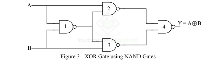
From the logic circuit diagram of the XOR gate using NAND gates only, it is clear that we require 4 NAND gates.
Now, let us understand how this NAND logic circuit functions to produce an output equivalent to the XOR gate.
The output of the first NAND gate is,
$$\mathrm{Y_{1} \: = \: \overline{A \: B}}$$
The outputs of the secondary and third NAND gates are,
$$\mathrm{Y_{2} \: = \: \overline{A \cdot \overline{AB}}}$$
$$\mathrm{Y_{3} \: = \: \overline{B \cdot \overline{AB}}}$$
Finally, these two outputs (Y2 and Y3) are connected to the fourth NAND gate. This NAND gate will produce an output which is,
$$\mathrm{Y \: = \: \overline{\overline{A \cdot \overline{AB}} \cdot \overline{B \cdot \overline{AB}}}}$$
$$\mathrm{\Rightarrow \: Y \: = \: A \cdot \overline{AB} \: + \: B \cdot \overline{AB} \: = \: A(\bar{A} \: + \: \bar{B}) \: + \: B(\bar{A} \: + \: \bar{B})}$$
$$\mathrm{\Rightarrow \: Y \: = \: A \: \bar{A} \: + \: A \: \bar{B} \: + \: \bar{A} \: B \: + \: B \: \bar{B}}$$
$$\mathrm{\therefore \: Y \: = \: A \: \bar{B} \: + \: \bar{A} \: B \: = \: A \oplus B}$$
This is the output of the XOR gate. Hence, in this way, we can implement the XOR gate from NAND gates only.
Implementation of XNOR Gate from NAND Gate
As we know, the NAND Gate is a universal logic gate, using which we can implement any other type of logic gate or logical expression. Read this tutorial to find out how you can implement an XNOR gate using only NAND gates. Let's start with a basic overview of XNOR and NAND gates.
What is an XNOR Gate?
The XNOR (Exclusive-NOR) Gate is a type of derived logic gate. The XNOR gate is a logic gate that has two inputs and one output. The XNOR gate produces a HIGH (Logic 1) output when both of its inputs are equal, i.e. either HIGH (Logic 1) or LOW (Logic 0).
When the inputs of the XNOR gate are different, i.e., one is HIGH (Logic 1) and another is LOW (Logic 0), then the output of the XNOR gate is a LOW (Logic 0) state. The logic symbol of the XNOR gate is shown in Figure-1.

Hence, the XNOR gate produces an output HIGH (Logic 1) only when both of its inputs are equal. Thus, the XNOR gate is also known as "equality detector".
The output of the XNOR gate is given by,
$$\mathrm{Y \: = \: A \odot B \: = \: AB \: + \: \bar{A} \: \bar{B}}$$
Where, A and B are the two input variables to the XNOR gate, Y is the output variable of the XNOR gate. The output expression of the XNOR gate is read as Y is equal to A ex-nor B.
Truth Table of XNOR Gate
The truth table shows the relationship between inputs and output of the XNOR gate. The truth table of an XNOR gate is shown below.
| Input | Output | |
|---|---|---|
| A | B | Y = (AB + A'B') |
| 0 | 0 | 1 |
| 0 | 1 | 0 |
| 1 | 0 | 0 |
| 1 | 1 | 1 |
What is a NAND Gate?
The NAND Gate is a type of universal logic gate. Where, a universal logic gate is one that can be used to realize any kind logical expression or any other type of logic gate.
A NAND gate is basically a combination of two basic logic gates namely AND gate and NOT gate, i.e.,
$$\mathrm{NAND \: Logic \: = \: AND \:Logic \: + \: NOT \: Logic}$$
A NAND gate is the type of logic gate whose output is LOW (Logic 0) when all its inputs are high, and its output is HIGH (Logic 1), when any of its inputs is LOW (Logic 0). Therefore, the operation of the NAND gate is opposite that of the AND gate. The logic symbol of a two input NAND gate is shown in Figure-2.

Output Equation of NAND Gate
If A and B are the input variables and Y is the output variable of the NAND gate, then its output is given by,
$$\mathrm{Y \: = \: \overline{A \cdot B} \: = \: (A \cdot B)'}$$
It is read as "Y is equal to A·B whole bar".
Truth Table of NAND Gate
The following is the truth table of the NAND gate −
| Input | Output | |
|---|---|---|
| A | B | Y = (A·B)' |
| 0 | 0 | 1 |
| 0 | 1 | 1 |
| 1 | 0 | 1 |
| 1 | 1 | 0 |
Now, let us discuss the implementation of XNOR Gate from NAND Gate.
Implementation of XNOR Gate from NAND Gate
As discussed above, the NAND gate is a universal logic, using which we can implement any other type of logic gate. The realization of XNOR gate using NAND gates is shown in Figure-3.

From the logic circuit diagram of the XNOR gate using NAND gates only, it is clear that we require 5 NAND gates.
Now, let us understand how this NAND logic circuit functions to produce an output equivalent to the XNOR gate −
The output of the first NAND gate is,
$$\mathrm{Y_{1} \: = \: \overline{A \: B}}$$
The outputs of the secondary and third NAND gates are,
$$\mathrm{Y_{2} \: = \: \overline{A \cdot \: \overline{AB}}}$$
$$\mathrm{Y_{3} \: = \: \overline{B \cdot \: \overline{AB}}}$$
These two outputs (Y2 and Y3) are connected to the fourth NAND gate. This NAND gate will produce an output which is,
$$\mathrm{Y \: = \: \overline{\overline{A \cdot \: \overline{AB}} \cdot \overline{B \cdot \overline{AB}}}}$$
$$\mathrm{\Rightarrow \: Y \: = \: A \cdot \overline{AB} \: + \: B \cdot \overline{AB} \: = \: A(\bar{A} \: + \: \bar{B}) \: + \: B(\bar{A} \: + \: \bar{B})}$$
$$\mathrm{\Rightarrow \: Y \: = \: A \: \bar{A} \: + \: A \: \bar{B} \: + \: \bar{A} \: B \: + \: B \: \bar{B}}$$
$$\mathrm{\therefore \: Y \: = \: A \: \bar{B} \: + \: \bar{A} \:B \: = \: A \oplus B}$$
Finally, the output of the fourth NAND gate is input to the fifth NAND gate that functions as an inverter, and produces an output equivalent to the XNOR gate, i.e.,
$$\mathrm{Y \: = \: \overline{A \oplus B} \: = \: A \odot B}$$
This is the output of the XNOR gate. Therefore, in this way, we can implement the XNOR gate from NAND gates only.
Implementation of NOT Gate from NOR Gate
A NOT Gate is a basic logic gate that gives an output which is complement of its input. A NOR gate is a universal logic gate that can be used to implement any other type of logic gate. A NOR gate is basically an OR gate followed by a NOT gate.
Read this tutorial to find out how you can implement a NOT gate using NOR gate. Let's start the discussion with a brief overview of NOT and NOR gates.
What is a NOT Gate?
In digital electronics, a NOT gate is a basic logic gate that has only one input and one output. It is type of logic gate whose output is always the complement of its input. Therefore, the NOT gate is also known as an inverter.
If the input of the NOT gate is LOW (Logic 0), then it gives an output that is HIGH (Logic 1). If the input is HIGH (Logic 1), then the NOT gate gives the LOW (logic 0) output. The logic symbol of the NOT gate is shown in Figure-1.

The NOT operation is represented by the '-' (bar) symbol. Therefore, if the input variable of the NOT gate is A, then its output Y is given by,
$$\mathrm{Y \: = \: \bar{A} \: = \: A' }$$
Truth Table of NOT Gate
The truth table of the NOT gate gives the relationship between its input variable and output variable. The following is truth table of the NOT gate −
| Input (A) | Output (Y = A') |
|---|---|
| A | B |
| 0 | 1 |
| 1 | 0 |
What is a NOR Gate?
NOR gate is a type of universal gate, therefore, it can be used to implement any other type of logic gate. NOR gate is basically a combination of NOT gate and OR gate, i.e. OR gate followed by a NOT gate is a NOR gate. Thus,
$$\mathrm{NOR \: Gate \: = \: OR \: Gate \: = \: NOT \: Gate}$$
A NOR gate can accept any number of inputs and gives a single output. The output of the NOR gate is assumed HIGH or Logic 1, only when all of its inputs are LOW or Logic 0. For any other combination of inputs, the output of the NOR gate is assumed LOW or Logic 0. The logic symbol of a two input NOR gate is shown in Figure-2.

The operation of the NOR Gate is expressed by,
$$\mathrm{Y \: = \: \overline{A \: + \: B} \: = \: (A \: + \: B)'}$$
Where, A and B are the input variables and Y is the output variable of the NOR gate. The output expression of the NOR gate is read as "Y is equal to A plus B whole bar".
Truth Table of NOR Gate
For different combinations of inputs, we can analyze the operation of the NOR gate using its truth table, which is given below.
| Input | Output | |
|---|---|---|
| A | B | Y = (A + B)' |
| 0 | 0 | 1 |
| 0 | 1 | 0 |
| 1 | 0 | 0 |
| 1 | 1 | 0 |
Now, let us discuss the implementation of NOT Gate using NOR Gate.
Implementation of NOT Gate from NOR Gate
As discussed above, a NOR gate is a universal gate, therefore, we can use it to realize any other type of logic gate. The implementation of NOT gate from NOR gate is shown in Figure-3.
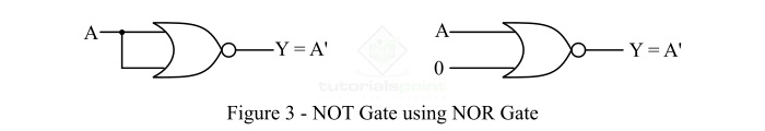
Hence, to realize the NOT gate using NOR gate, we simply join all its inputs terminals together and apply the signal to be NOTed or inverted to this common input terminal.
Also, we can use the NOR gate as a NOT gate by connecting all its input terminals except one to Logic 0, and applying the signal to be inverted to the remaining terminal. This configuration of NOR Gate as NOT Gate is referred to as a controlled inverter.
Hence, in this way, the NOT gate can be implemented using a NOR gate only.
Implementation of OR Gate from NOR Gate
An OR Gate is a basic logic gate that gives a HIGH or Logic 1 output, when any of its inputs is HIGH. Whereas, the NOR gate is a universal logic gate, which gives a HIGH output only when all its inputs are LOW or Logic 0. Before, going into the implementation of OR Gate using NOR Gate, let us discuss the basic theory of OR gate and NOR gate first.
What is an OR Gate?
An OR Gate is a basic logic gate. An OR gate can have two or more than two inputs, but has only one output. The OR gate gives a HIGH (Logic 1) output if any one of its inputs is in the HIGH or Logic 1 state, otherwise, it gives a LOW (Logic 0) state as output. Therefore, the output of the OR gate is LOW or Logic 0 state, only if all its inputs are LOW or Logic 0 state.
The OR gate is also known as an "any or all gate" or "an inclusive OR gate". The logic symbol of a two input OR gate is shown in Figure-1.

If variables A and B are the inputs to the OR gate and Y is the output variable, then the output equation of the OR gate is given by,
$$\mathrm{Y \: = \: A \: + \: B}$$
Where, the '+' symbol represents the OR operation. It is read as "Y is equal to A OR B".
The table that show the relationship between inputs and output of an OR gate is referred to as a truth table of the OR gate.
Truth Table of OR Gate
The following is the truth table for the OR Gate.
| Input | Output | |
|---|---|---|
| A | B | Y = A + B |
| 0 | 0 | 0 |
| 0 | 1 | 1 |
| 1 | 0 | 1 |
| 1 | 1 | 1 |
What is a NOR Gate?
NOR Gate is a universal logic gate, and hence it can be used for implementation of any other type of logic gate.
NOR means NOT + OR. That means, the OR output is NOTed or inverted. Therefore, the NOR gate is a combination of OR gate and a NOT gate, i.e.,
$$\mathrm{NOR \:Gate \: = \:OR \: Gate \: = \: NOT \: Gate}$$
A NOR gate is a type of logic gate whose output is HIGH (Logic 1), only when all its inputs are LOW (Logic 0), and it gives an output LOW (Logic 0), even if any of its inputs becomes HIGH (Logic 1). The logic symbol of a two input NOR gate is shown in Figure-2.

If variables A and B are the input variables to the NOR gate and Y is the output variable of the NOR gate, then the output of the NOR gate is given by,
$$\mathrm{Y \: = \: \overline{A \: + \: B} \: = \: (A \: + \: B)'}$$
It is read as "Y is equal to A plus B whole bar".
Truth Table of NOR Gate
The following is the truth table of the NOR gate −
| Input | Output | |
|---|---|---|
| A | B | Y = (A + B)' |
| 0 | 0 | 1 |
| 0 | 1 | 0 |
| 1 | 0 | 0 |
| 1 | 1 | 0 |
Now, let us discuss the implementation of OR Gate from NOR Gate.
Implementation of OR Gate from NOR Gate
As we know, the NOR gate is a type of universal logic gate, therefore, using NOR gates only, we can implement the OR operation. The logic diagram of OR Gate using NOR Gate is shown in Figure-3.

Hence, from the logic circuit, it is clear that we require only two NOR gates for the realization of OR operation.
The first NOR gate performs the NOR operation on variables A and B, thus the output of the first NOR gate is,
$$\mathrm{Y_{1} \: = \: \overline{A \: + \: B}}$$
The second NOR gates perform the NOT operation on the output of the first NOR gate. Therefore, the output of the second NOR gate is,
$$\mathrm{Y \: = \: A \: + \: B}$$
This is the output expression of an OR gate. Therefore, we can realize an OR gate using NOR gates only as shown in Figure-3.
Implementation of AND Gate from NOR Gate
An AND Gate is a basic logic gate that performs the binary multiplication, i.e., it gives a HIGH or Logic 1 output, only when all its inputs are in HIGH or Logic 1 state. On the other hand, a NOR gate is a type of universal logic gate. Therefore, NOR gate can be used to realize any other type of logic gate.
Before going into the implementation of AND gate using NOR gates only, let us discuss the basic theory of AND Gate and NOR Gate first.
What is an AND Gate?
An AND Gate is a basic logic gate. An AND gate may have two or more than two inputs, but gives only one output. The AND gate gives a LOW (Logic 0) output if any one of its inputs is in the LOW or Logic 0 state, otherwise, it gives a HIGH (Logic 1) state as output. Therefore, the output of the AND gate is HIGH or Logic 1 state, only if all its inputs are HIGH or Logic 1 state.
The AND gate is also known as an "all or nothing gate". The logic symbol of a two input AND gate is shown in Figure-1.

If variables A and B are inputs to the AND gate and Y is the output variable of the AND gate, then the output equation of the AND gate is given by,
$$\mathrm{Y \: = \: A\cdot B}$$
Where, the '.' (dot) symbol represents the AND operation. It is read as "Y is equal to A AND B".
Truth Table of AND Gate
The table that show the relationship between inputs and output of the AND gate is referred to as the truth table of AND gate. The following is the truth table of the AND Gate −
| Input | Output | |
|---|---|---|
| A | B | Y = A · B |
| 0 | 0 | 0 |
| 0 | 1 | 0 |
| 1 | 0 | 0 |
| 1 | 1 | 1 |
What is a NOR Gate?
NOR Gate is a type of universal logic gate, because this logic gate can be used for realization of any other type of logic gate.
NOR means NOT + OR. That means, the OR output is NOTed or inverted. Therefore, the NOR gate is a combination of OR gate and a NOT gate, i.e.,
$$\mathrm{NOR \: Gate \: = \: OR \: Gate \: + \: NOT \: Gate}$$
A NOR gate is a type of logic gate whose output is HIGH (Logic 1), only when all its inputs are LOW (Logic 0), and it gives an output LOW (Logic 0), even if any of its inputs become HIGH (Logic 1). The logic symbol of a two input NOR gate is shown in Figure-2.

If variables A and B are the input variables and Y is the output variable of the NOR gate, then the output of the NOR gate is given by,
$$\mathrm{Y \: = \: \overline{A \: + \: B} \: = \: (A \: + \: B)'}$$
It is read as "Y is equal to A plus B whole bar".
Truth Table of NOR Gate
The following is the truth table of the NOR gate −
| Input | Output | |
|---|---|---|
| A | B | Y = A · B |
| 0 | 0 | 1 |
| 0 | 1 | 0 |
| 1 | 0 | 0 |
| 1 | 1 | 0 |
Now, let us discuss the implementation of AND Gate from NOR Gate.
Implementation of AND Gate from NOR Gate
As mentioned above that the NOR gate is a logic gate, therefore, we may use it to realize an AND gate. The realization of an AND gate from the NOR gates only is shown Figure-3.

Thus, for the realization of an AND gate from NOR gate, we require 3 NOR gates. Where, the first two NOR gates are used to complement the input variables A and B, and the third NOR gate is used to produce an output equivalent to the AND operation.
Output Equation
The outputs of the first two NOR gates are,
$$\mathrm{Y_{1} \: = \: \bar{A}}$$
$$\mathrm{Y_{2} \: = \: \bar{B}}$$
The output of the third NOR gate is,
$$\mathrm{Y \: = \: \overline{\bar{A} \: + \: \bar{B}} \: = \: \bar{\bar{A}} \cdot \bar{\bar{B}} \: = \: A \cdot B} $$
This is the output of an AND gate. Hence, the logic circuit using NOR gates shown in Figure-3 is equivalent to the AND gate.
Difference between NAND Gate and NOR Gate
In digital electronics, logic gates are the basic building blocks of all digital circuits that act as the switching devices in the digital circuits. Therefore, a logic gate is a digital circuit used to perform several logical operations in a digital device or system. A logic gate can accept one or multiple inputs but produces only a single output. Where, the output of a logic gate is determined by the combination of input signals. The operation of the logic gates is based on the Boolean algebra.
These days, logic gates are being used in every digital electronic device such as smartphones, laptops, computers, memories, etc. There are many types logic gates available such as AND gate, OR gate, NOT gate, NAND gate, NOR gate, XOR gate, XNOR gate, etc.
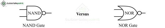
Here, we will highlight all the differences between NAND gate and NOR gate. Both the NAND gate and the NOR gate are universal logic gates, which means we can implement any logical expression by using the NAND and NOR gates only. Before getting into the differences, let's start with some basics.
What is a NAND Gate?
A NAND gate basically a combination of NOT gate and AND gate, i.e. NOT + AND = NAND. Therefore, the NAND gate is a negated version of AND gate.
For a NAND gate, the output of the gate is high (1), when all of its inputs are low (0) or at least one input is low. If it has all the inputs low (0), then the gate's output will be high (1). Hence, from the explanation, it is clear that the NAND gate is an exact inverse of the AND gate.
The logical or Boolean expression of a two input NAND gate is given by,
$$\mathrm{Y \: = \: \overline{A \cdot B} \: = \: (A \cdot B)^\prime}$$
Where, Y is the output of the NAND gate and A and B are the binary inputs.
The NAND gate follows the commutative law, i.e.
$$\mathrm{(A \: \cdot \: B)^\prime \: = \: (B \: \cdot \: A)^\prime}$$
Hence, from the Boolean expression of the NAND gate, we can see that the output of the NAND gate is obtained by multiplying all the inputs and then by taking the compliment of the multiplied result.
The following is the truth table of a two input NAND gate −
| Inputs | AND | Output | |
|---|---|---|---|
| A | B | A·B | Y = (A·B)' |
| 0 | 0 | 0 | 1 |
| 0 | 1 | 0 | 1 |
| 1 | 0 | 0 | 1 |
| 1 | 1 | 1 | 0 |
NAND gates are used in realizing other logic gates, making flip-flops, registers, burglar alarm circuit, freezer warning buzzer, etc.
What is a NOR Gate?
The NOR gate is a combination of NOT and OR gates, i.e. OR + NOT = NOR. A NOR gate consists of an OR gate followed by a NOT gate.
For the NOR gate, the output of the gate is high (1), when all its inputs are low (0). In all other cases, it produces a low output. Thus, the NOR gate is nothing but a negated version of the OR gate.
The Boolean expression of a two input NOR gate is given by,
$$\mathrm{Y \: = \: \overline{A \: + \: B} \: = \: (A \: + \: B)^\prime}$$
Where, Y is the gate's output and A & B are the inputs. Hence, from the Boolean expression of the NOR gate, it is clear that the gate's output can be obtained by the logical addition of all the inputs and then taking the complement of the result of addition.
The following is the truth table of a two input NOR gate −
| Inputs | OR | Output | |
|---|---|---|---|
| A | B | A+B | Y = (A+B)' |
| 0 | 0 | 0 | 1 |
| 0 | 1 | 1 | 0 |
| 1 | 0 | 1 | 0 |
| 1 | 1 | 1 | 0 |
The NOR gate is used in the realization of several combinational and sequential digital circuits like multiplexers, multipliers, counters, etc.
Difference between NAND Gate and NOR Gate
NAND and NOR gates are types of universal logic gates, however, there are several differences between these that are listed in the following table −
| Difference | NAND Gate | NOR Gate |
|---|---|---|
| Definition | A NAND gate is a universal logic gate which performs the negated logical multiplication. | A NOR gate is a universal logic gate which performs the negated logical addition. |
| Implementation | NAND gate can be implemented by using an AND gate followed by a NOT gate. | NOR gate can be implemented by using an OR gate followed by a NOT gate. |
| Representation | The operation of NAND gate can be represented by the complimented AND operation, i.e. (·)'. | The operation of a NOR gate can be represented by the complimented OR operation, i.e. (+)'. |
| Boolean Expression |
The Boolean expression of a two input NAND gate is given by, $\mathrm{Y \: = \: \overline{A \cdot B} \: = \: (A \: \cdot \: B)^\prime}$ |
The Boolean expression of a two input NOR gate is given by, $\mathrm{Y \: = \: \overline{A \: + \: B} \: = \: (A \: + \: B)^\prime}$ |
| Low Output | The NAND gate produces a low (0) output, when all its inputs are high. | The NOR gate produces a low (0) output, when all its inputs or at least one input is high (1). |
| High Output | The NAND gate produces a high (1) output, when all its inputs or at least one input is low (0). | The NOR gate produces a high (1) output, when all its inputs are low (0). |
| Applications | The NAND gate is used in constructing other logic gates, making flip-flops, registers, implementing burglar alarm circuit, freezer warning buzzer, etc. | The NOR gate is used in the implementation of various combinational and sequential digital circuits like multiplexers, multipliers, counters, etc. |
Conclusion
The most significant difference between these two gates is that the NAND gate executes a negated logical multiplication, while the NOR gate executes a negated logical addition.
Implementation of XOR Gate from NOR Gate
To carry out numerous logical processes, logic gates are crucial elements in the design of digital circuits. One such gate that generates a high output when the inputs are different from one another is the XOR (Exclusive OR) gate. Using NOR gates to create an XOR gate is an intriguing strategy that will be discussed in this tutorial. Understanding this implementation helps us better grasp the flexibility and relationships between logic gates.
What is a XOR Gate?
Another fundamental logic gate that is frequently utilised in digital circuits is the XOR (Exclusive OR) gate. When there are an odd number of HIGH inputs, it generates a HIGH output. To put it another way, the output is only HIGH when the inputs are different from one another.
Truth Table of XOR Gate
A two-input XOR gate's truth table is as follows −
| Input A | Input B | Output |
|---|---|---|
| 0 | 0 | 0 |
| 0 | 1 | 1 |
| 1 | 0 | 1 |
| 1 | 1 | 0 |
The Boolean expression for a two-input XOR gate is −
$$\mathrm{Output \: = \: A \: \oplus \: B}$$
Where '$\mathrm{\oplus}$' represents the XOR operation.
NOR Gate
A NOR gate is a type of logic gate that executes a logical disjunction (OR) and then a logical negation (NOT). It generates a single output signal from two or more input signals. Only when all of a NOR gate's inputs are LOW (0) will the output be HIGH (1), and for all other input configurations, the output will be LOW (0).
Truth Table of NOR Gate
A two-input NOR gate's truth table is as follows −
| Input A | Input B | Output |
|---|---|---|
| 0 | 0 | 1 |
| 0 | 1 | 0 |
| 1 | 0 | 0 |
| 1 | 1 | 0 |
The Boolean expression for a two-input NOR gate is −
$$\mathrm{Output \: = \: \thicksim \: (A \: + \: B)}$$
Where '~' represents logical negation (NOT) and '+' represents logical disjunction (OR).
Numerous more logic gates and intricate digital circuits can be implemented using NOR gates, which are frequently used in digital circuits. Since they are regarded as universal gates, any other logic gate or circuit can be built only out of NOR gates.
Implementation of XOR Gate from NOR Gate
It takes at least five NOR gates to create the circuit diagram for an XOR gate using only NOR gates. More than five NOR gates can also contain an XOR gate. The schematic for an XOR gate employing five NOR gates is shown in the accompanying figure.
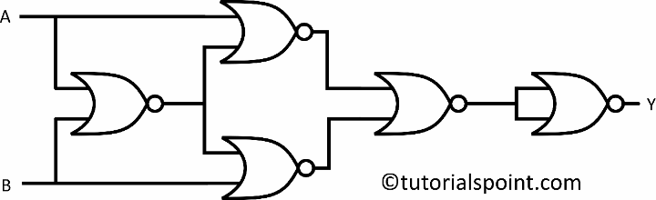
$$\mathrm{Y \: = \: (A \: \overline{B} \: + \: \overline{A} \: B)}$$
Here is how to obtain the output of XOR gate from the above circuit −
The leftmost NOR gate has inputs A and B and its output is $\mathrm{\overline{A+B}}$
Inputs for the upper NOR gate are A and $\mathrm{\overline{A+B}}$ and the output is $\mathrm{\overline{A \: + \: \overline{A+B}}}$
Again, the inputs for the lower NOR gate are B and $\mathrm{\overline{A+B}}$ and its output is $\mathrm{\overline{B \: + \: \overline{A+B}}}$
The inputs for the 4th NOR gate are the outputs of the upper and lower NOR gates i.e. $\mathrm{\overline{A \: + \: \overline{A+B}}}$ and $\mathrm{\overline{B \: + \: \overline{A+B}}}$
The output of the 4th NOR gate = $\mathrm{\overline{\overline{A \: + \: \overline{A+B}} \: + \: \overline{B \: + \: \overline{A+B}}}}$
$\mathrm{= \: \overline{\overline{A}\cdot \: \overline{(\overline{A \: + \: B})} \: + \: \overline{B}\cdot \: \overline{(\overline{A \: + \: B})}}}$
$\mathrm{\overline{\overline{A}\cdot \: (A \: + \: B) \: + \: \overline{B}\cdot \: (A \: + \: B)}}$
$\mathrm{\overline{\overline{A}\cdot \: A \: + \: \overline{A}\cdot \: B \: + \: \overline{B}\cdot \: A \: + \: \overline{B}\cdot \: B}}$
$\mathrm{\overline{\overline{A}\cdot \: B \: + \: \overline{B}\cdot \: A}}$
Now, this is the input for the last or 5th NOR gate. This NOR gate gives the output as the inversion of its input. Hence the final output of the above circuit is, $\mathrm{\overline{\overline{B\cdot \overline{A} \: + \: \overline{B}\cdot \: A}}}$ or, $\mathrm{Y \: = \: (A\cdot \overline{B} \: + \: \overline{A}\cdot \: B)}$
This is the output of the XOR gate. Hence the above NOR gate-based circuit is the circuit of XOR gate.
Thus the output of the above circuit is the same as the output of an XOR gate. Hence the above circuit represents the circuit diagram of Exclusive OR gate using NAND gates.
Implementation of XNOR Gate using NOR Gate
The NOR gate is a type of universal logic gate, hence we can use only NOR gates to realize the XNOR logic function.
Designing an XNOR Gate using NOR Gate
To design an XNOR gate using NOR gate, we first derive the XNOR logic function in terms of NOR logic as follows.
The output of XNOR gate is given by,
$$\mathrm{Y \: = \: AB \: + \: \bar{A} \: \bar{B}}$$
To implement an XNOR gate logic using NOR gate, we require a minimum of 4 NOR gates. The circuit diagram of XNOR gate from NOR gate is depicted in the following figure:
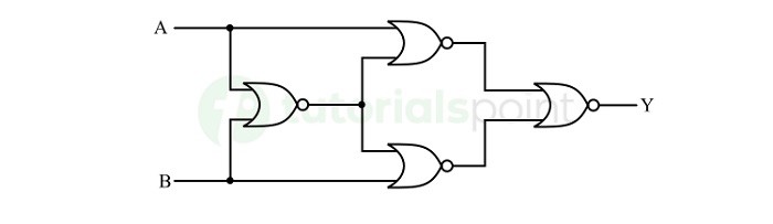
In this circuit, the output is
$$\mathrm{Y \: = \: \overline{\overline{A \: + \: \overline{(A \: + \: B)}} \: + \: \overline{B \: + \: \overline{(A \: + \: B)}}}}$$
$$\mathrm{Y \: = \: \overline{\overline{A \: + \: \overline{(A \: + \: B)}}} \: \cdot \: \overline{ \overline{B \: + \: \overline{(A \: + \: B)}}}}$$
$$\mathrm{Y \: = \: (A \: + \: \overline{(A \: + \: B)}) \: \cdot \: (B \: + \: \overline{(A \: + \: B)})}$$
$$\mathrm{Y \: = \: (A \: + \: (\bar{A} \: \cdot \: \bar{B})) \: (B \: + \: (\bar{A} \: \cdot \: \bar{B}))}$$
$$\mathrm{Y \: = \: (A \: + \: \bar{A}) \: (A \: + \: \bar{B}) \: (\bar{A} \: + \: B) \: (B \: + \: \bar{B})}$$
$$\mathrm{Y \: = \: (A \: + \: \bar{B}) \: (\bar{A} \: + \: B)}$$
$$\mathrm{Y \: = \: A\cdot\bar{A} \: + \: \bar{A}\cdot\bar{B} \: + \: A\cdot B \: + \: B\cdot\bar{B}}$$
$$\mathrm{\therefore \: Y \: = \: A\cdot B \: + \: \bar{A}\cdot\bar{B}}$$
This is the desired output of the XNOR gate. Thus, the above shown NOR logic circuit performs the XNOR operation.
Implementation of NAND/NOR gate using CMOS
In digital electronics, NAND and NOR gates are two universal logic gates that are used to perform Boolean operations on multiple input variables. These gates produce an output based on the combination of inputs applied.
NAND and NOR gates are used as the fundamental building blocks in the digital circuits and systems. We can design and implement the NAND and NOR gates in different technologies such as DTL, RTL, TTL, and CMOS. This chapter deals with implementation of NAND and NOR gates using CMOS technology.
In CMOS (Complementary Metal Oxide Semiconductor) technology, the NAND and NOR logic gates are designed by connecting NMOS and PMOS transistors in series and parallel connections. The block diagram of a 2-input logic gate in CMOS technology is shown in the following figure.
Before getting deeper into the NAND and NOR gate using CMOS technology. Lets first study the basics of NAND and NOR gates individually.
NAND Gate
The NAND gate is a combination of NOT gate and AND gate, where a NOT gate connected to the output of the AND gate. Thus, it is also known as NOTed AND gate.
$$\mathrm{AND \: Gate \: + \: NOT \: Gate \: = \: NAND \: Gate}$$
The logic circuit symbol of a two input NAND gate is shown in the following figure −
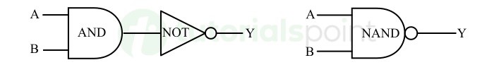
The NAND gate produces a low or logic 0 output when all inputs applied to it are high or logic 1. For all other input combinations, it produces a high or logic 1 output.
Truth Table of NAND Gate
The truth table of a two input NAND gate is shown here −
| Inputs | Output | |
|---|---|---|
| A | B | Y |
| 0 | 0 | 1 |
| 0 | 1 | 1 |
| 1 | 0 | 1 |
| 1 | 1 | 0 |
From this truth table, we can write the Boolean expression of the NAND gate, as follows.
$$\mathrm{Y \: = \: \overline{A\cdot B}}$$
Here, Y is the output variable, and A and B are the input variables.
NOR Gate
The NOR gate is a universal logic gate in digital electronics. It is a combination of two basic logic gates namely, NOT gate and OR gate, where it is realized by connecting a NOT gate to the output of the OR gate. Therefore,
$$\mathrm{OR \: Gate \: + \: NOT \: Gate \: = \: NOR \: Gate}$$
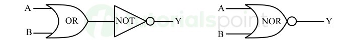
The output of the NOR gate is high or logic 1, when all its inputs are low or logic 0. For all other input combinations, the output of the NOR gate is low or logic 0.
Truth Table of NOR Gate
The following is the truth table of a two input NOR gate that describing its operation −
| Inputs | Output | |
|---|---|---|
| A | B | Y |
| 0 | 0 | 1 |
| 0 | 1 | 0 |
| 1 | 0 | 0 |
| 1 | 1 | 0 |
From this truth table, we can write the Boolean expression of the NOR gate, as follows.
$$\mathrm{Y \: = \: \overline{A \: + \: B}}$$
Here, Y is the output variable, and A and B are the input variables.
This is all about the basics of NAND and NOR gate. Let us now discuss the implementation of NAND and NOR gates using CMOS technology.
NAND Gate Using CMOS Technology
The NAND gate can be implemented in CMOS technology by using PMOS and NMOS transistors. The circuit diagram of a two input NAND gate in CMOS technology is shown in the following figure −
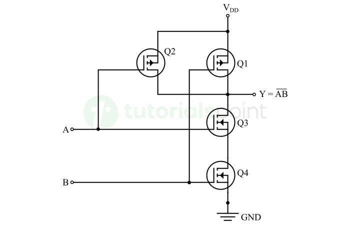
It consists of two PMOS transistors Q1 and Q2 and two NMOS transistors Q3 and Q4. The PMOS transistors are connected in parallel between the power supply VDD and the output terminal Y. Similarly, the NMOS transistors are connected in series between the output terminal Y and the ground terminal GND.
Now, let us understand the operation of this CMOS NAND gate.
Case 1: When Input A is Low and Input B is Low
In this case, when both inputs A and B are low, the PMOS transistors Q1 and Q2 are ON and the NMOS transistors Q3 and Q4 are OFF. Hence, there is a closed path between the supply voltage VDD and the output terminal Y.
Thus, the output Y will be connected to the voltage level VDD. Also, there is no path between the output terminal and the ground terminal as both NMOS transistors are OFF. Under this condition, the output line will maintain the voltage level at VDD, which indicates the output High.
Thus, when A = 0 and B = 0, then Y = 1
Case 2: When Input A is Low and Input B is High
In this case, the PMOS transistor Q1 will be ON while the PMOS transistor Q2 will be OFF. The NMOS transistor Q3 will be OFF and the NMOS transistor Q4 will be ON.
For this switching condition of the CMOS transistors, the power supply VDD will get a path to the output terminal through the PMOS transistor Q1. Since, the NMOS transistor Q3 and Q4 are connected in series and the NMOS transistor Q3 is OFF. Hence, there is no path between the output terminal and the ground terminal.
Therefore, the output terminal Y maintain the voltage level at VDD and results in a High output.
Thus, when A = 0 and B = 1, then Y = 1
Case 3: When Input A is High and Input B is Low
In this case, the PMOS transistor Q1 will be OFF and the PMOS transistor Q2 will be ON. The NMOS transistor Q3 will be ON and the NMOS transistor Q4 will be OFF.
Under this switching condition of the CMOS transistors, the output terminal will connect to the power supply through the PMOS transistor Q2. Since, both NMOS transistors are connected in series and the NMOS transistor Q4 is OFF. Hence, there is no path between the output terminal and the ground terminal.
Therefore, the output line will maintain the voltage level at VDD and results in a High output.
Thus, when A = 1 and B = 0, then Y = 1
Case 4: When Input A is High and Input B is High
In this case, both PMOS transistors Q1 and Q2 will be OFF and both NMOS transistors will be ON. In this case, there is no path between the output terminal and the power supply VDD, but there is a direct path between the output terminal and the ground terminal. This results in a ground voltage level at the output terminal and produces a Low output.
Hence, when A = 1 and B = 1, then Y = 0
The operation of this CMOS NAND gate is shown in the following truth table −
| Inputs | Output | |
|---|---|---|
| A | B | Y |
| Low (0) | Low (0) | High (1) |
| Low (0) | High (1) | High (1) |
| High (1) | Low (0) | High (1) |
| High (1) | High (1) | Low (0) |
This is all about NAND gate implementation using CMOS technology and its operation for different input combinations.
Let us now discuss the implementation and operation of NOR gate using CMOS technology.
NOR Gate Using CMOS Technology
Similar to CMOS NAND gate, we can also design a NOR gate using PMOS and NMOS transistors. The circuit diagram of a two input NOR gate using CMOS technology is shown in the following figure −

This CMOS NOR gate is designed by using two PMOS transistors Q1 and Q2 and two NMOS transistor Q3 and Q4. Where the PMOS transistors are connected in series between the supply voltage VDD and the output terminal Y. The NMOS transistors are connected in parallel between the output terminal Y and the ground terminal GND.
Now, let us understand how does this CMOS circuit operate as a two input NOR gate.
Case 1: When Input A is Low and Input B is Low
In this case, both PMOS transistors Q1 and Q2 will be ON and both NMOS transistors Q3 and Q4 will be OFF.
Under this switching condition of the CMOS transistors, there is a path between the supply voltage VDD and the output terminal Y through the ON PMOS transistors. But there is no path between the output terminal Y and the ground terminal GND. This maintains the output at the voltage level VDD and hence the output will be High.
Thus, when A = 0 and B = 0, then Y = 1
Case 2: When Input A is Low and Input B is High
In this case, the PMOS transistor Q1 is ON, the PMOS transistor Q2 is OFF, the NMOS transistor Q3 is OFF, and the NMOS transistor Q4 is ON.
Since, the PMOS transistors Q1 and Q2 are connected in series and the transistor Q2 is OFF. Thus, there is no path between the power supply VDD and the output terminal Y. But there is a connection between the output line Y and the ground terminal GND through the ON NMOS transistor Q4. This sets the output terminal to ground voltage and makes the output Low.
Therefore, when A = 0 and B = 1, then Y = 0
Case 3: When Input A is High and Input B is Low
In this condition, the PMOS transistor Q1 is OFF, the PMOS transistor Q2 is ON, the NMOS transistor Q3 is ON, and the NMOS transistor Q4 is OFF.
In this case, there is no closed path between the power supply VDD and the output line Y due to OFF PMOS transistor Q1. But there is a closed between the output line Y and the ground terminal GND through the ON NMOS transistor Q3. Hence, the output terminal is connected to the ground potential and makes the output Low.
Thus, when A = 1 and B = 0, then Y = 0
Case 4 When Input A is High and Input B is High
In this case, both PMOS transistors Q1 and Q2 are OFF and both NMOS transistors Q3 and Q4 are ON. Under this condition, there is no path between the supply voltage VDD and the output terminal Y. But there is a closed path between the output terminal Y and the ground terminal GND. This maintains the output line at ground voltage level and hence the output will be Low.
Thus, when A = 1 and B = 1, then Y = 0
This complete operation of the CMOS NOR gate can be summarized in the form of a truth table which is given below.
| Inputs | Output | |
|---|---|---|
| A | B | Y |
| Low (0) | Low (0) | High (1) |
| Low (0) | High (1) | Low (0) |
| High (1) | Low (0) | Low (0) |
| High (1) | High (1) | Low (0) |
Advantages of NAND and NOR Gates using CMOS Technology
NAND and NOR gates implemented in CMOS technology offer several benefits over other technologies. Some of the key advantages of CMOS NAND and NOR gates are listed here −
- CMOS NAND and NOR gates consume relatively low power. This advantage makes these logic gates well-suited to use in battery powered devices.
- NAND and NOR gates designed using CMOS technology have high immunity against noise and interference. They can be designed to have a wider range of operating voltage.
- The CMOS technology offers high-density integration that allows for implementing a large number of NAND and NOR gates on a single chip. These gates provide symmetrical output characteristics that allow them to integrate with different types of digital circuits seamlessly.
- CMOS technology is one of the well-established, mature, and cost-effective semiconductor manufacturing technology. Hence, the CMOS NAND and NOR gates are relatively easy to manufacture and cost effective.
Applications of CMOS NAND and NOR Gates
The CMOS NAND and NOR gates are widely used in the following applications due to their benefits and versatility −
- CMOS NAND and NOR gates are widely used in the logic circuit designs to perform logical operations.
- In digital systems, the CMOS NAND and NOR gates are used to implement arithmetic circuits like adders, subtractors, multipliers, etc.
- They are also used in memory units to implement memory cell structures.
- CMOS NAND and NOR gates are also used to design multiplexers and demultiplexers.
- Some other common applications of CMOS NAND and NOR gates include digital signal processing, digital timing circuits, analog to digital conversion, digital communication, etc.
Conclusion
The CMOS NAND and NOR gates are widely used in a variety of applications in the field of digital electronics. This type of NAND and NOR gates offer several advantages such as high efficiency, low power consumption, versatility, low cost, high reliability, etc.
In this chapter, we explained the implementation of NAND and NOR gates using CMOS technology along with their advantages and applications.
Memory Devices
Memory is one of the important parts in a computer or any other digital system. It is used to hold data and programs required for processing and performing tasks.
Memory also affects the performance, efficiency, and speed of the digital system. These days, semiconductor memories are popular, as they provide a very high-speed operation, large storage capacity, and compact size.
Here, we will explain the basic to advanced concepts related to semiconductor memory devices.
What is Memory?
In the field of digital electronics, the memory is a device that is used to store data and instruction in the digital systems like computers and other microprocessor-based systems. In modern digital systems, the memory is made up of semiconductor materials and known as semiconductor memory.
The memory is the device that provides the storage space in computer or any other digital system where data is to be processed and instructions required for processing are stored.
The memory is divided into a large number of small parts. Each part is called a memory cell. Each memory cell or location has a unique address assigned to it which varies from zero to total memory size minus one.
For example, if a computer has 64 kB memory size, then this memory unit has 64 1024 = 65536 memory location or cells. Hence, the address of these locations ranges from 0 to 65535.
Classification of Memory
Memory is primarily classified into two types, they are: Internal Memory and External Memory.
Internal Memory
Internal memory is also known as primary memory, as it is directed connected to the hardware architecture of the digital system. It is typically installed in the systems motherboard in form of ICs.
Examples of internal memory include cache memory, RAM (Random Access Memory), ROM (Read Only Memory), etc.
External Memory
External memory is also known as secondary memory. This memory is not directly connected to the hardware architecture of the systems, instead it is connected through cables as a peripheral device.
The external memory is primarily used to provide additional storage space to store data and instructions permanently. Examples of external memory are CD, DVD, HDD, SSD, USB drives, etc.
Memory Hierarchy
Memory hierarchy is defined as an arrangement of different types of memory devices used in a digital system depending on their characteristics, primarily speed and capacity. The memory hierarchy helps us to select an appropriate memory to use in our system at a specific level.
A typical memory hierarchy of memory for different memory devices is shown in the following figure −

Some of key characteristics of this memory hierarchy, when we go from top to bottom −
- Capacity in terms of storage increases.
- Cost per bit of storage decreases.
- Frequency of access of the memory by the CPU decreases.
- Access time by the CPU increases.
Functional Block Diagram of Memory
A memory is basically a group of multiple storage cells having a support circuit to perform data read/write operations. The following figure depicts the functional block diagram of a typical memory device −

It consists of the following main parts −
Address Lines
These lines are used to load the address of a specific memory location or cell.
Data Lines
These lines are used to read and write the data from/to the memory cell.
Read and Write Signal (R/W)
This signal is used to read and write the data from and to the memory cells. When the R signal is high, the data of the selected cell gets loaded on the data line. When the W line goes low, the data on the data line is loaded into the selected memory cell.
Chip Select Signal (CS)
This signal is used to enable or disable the memory chip. It is an active low signal, which means when this signal goes low, the memory chip is enabled and allow the read and write operations to execute. Otherwise, the memory chip will be disabled.
Important Terms Related to Memory Operation
The following are some important terms and definitions which are related to the read and write operations of memory −
- Write Cycle Time − The write cycle time is defined as the minimum amount of time for which a valid cell address is available for data writing operation in the cell. Typically, it is of the order of 200 ns.
- Write Pulse Time − The minimum duration of a write pulse is termed as write pulse time and it is of the order of 120 ns.
- Write Release Time − The minimum time for which the memory address is valid before the write pulse is known as write release time.
- Data Setup Time − The minimum amount of time for which the data remains valid before the write pulse ends is known as data setup time. Typically, it is around 120 ns.
- Data Hold Time − The minimum amount of time for which the data remains valid after the write pulse ends is known as data hold time.
- Read Cycle Time − The minimum amount of time for which a valid memory address remains available for reading the data from a memory cell is known as read cycle time. It is typically of the order of 200 ns.
- Access Time − The amount of time required to access data from a memory cell is referred to as access time of the memory. It is also of the order of 200 ns.
- Read to Output Active Time − The minimum time that required for enabling the output buffer after starting of the read pulse is called the read to output active time. Typically, this time is of the order of 20 ns.
- Read to Output Valid Time − The maximum delay time between the beginning of the read pulse and the availability of the valid data at the data output line is known as "read to output valid time".
These are some key terms whose knowledge is required to understand the read and write operations of a memory device.
Characteristics of Memory Devices
In this section, we will focus on studying some key characteristics of memory devices and their definitions and importance −
Storage Capacity
This parameter denotes the total memory of the device. It is generally expressed in terms of number of Bytes that it can store. For example, a memory of 1k 8 bits can store 1024 8 = 8192 Bytes of digital data.
Unit of Data Transfer
The number of bits that can be read or written in a single read or write cycle is called the unit of data transfer. In general, the unit of data transfer is equal to the word length or size of the data bus of the processor.
Modes of Access
It refers to the way in which the data can be read or write to the memory. There are following three modes used in digital memory devices −
Sequential Access
In this mode, the data is read from or write to the memory in a predefined sequential manner. In other words, to access the second file, we first access the first file, to access the third file, firstly access the first and second files, and so on.
Random Access
In this mode, we can directly access any memory location in any order.
Direct Access
This mode is a combination of sequential and random access modes. It is also termed as semi-random access mode.
Data Transfer Rate
It is defined as the amount of data that is read or write in one second. It is generally measured in bits per second. Data transfer rate is referred to as bandwidth of memory.
Types of Memory Devices
Some of the important classifications of memory devices used in computers and digital systems are listed and explained here.
Classification of memory on the basis of nature of data storage −
- Volatile Memory
- Non-Volatile Memory
Classification of memory on the basis of access modes −
- Sequential Access Memory
- Random Access Memory
Now, let us discus all these types of memories in detail along with their subtypes and characteristics.
Volatile Memory
A type of memory that requires continuous power supply to maintain the stored data is called a volatile memory. If the power supply to the memory is turned off, the data stored in it will be lost. Therefore, it is also termed as temporary memory.
Properties of Volatile Memory
The volatile memory loses its stored data when power supply to it is turned off. Volatile memory has fast operational speed; thus, it can read and write data in a short span of time.
Volatile memory is used to store data required to be accessed and perform operations. RAM (Random Access Memory) is an example of volatile memory.
Non-Volatile Memory
A type of memory which can retain stored data even when no power supply is present is known as non-volatile memory. It is also known as permanent memory and is used for long-term storage of digital data.
Properties of Non-Volatile Memory
Non-volatile memory stores data permanently. It can retain the stored data even when the power supply is switched off.
Non-volatile memory is slower than volatile memory. Hence, this memory has longer read and write cycles.
Examples of non-volatile memory includes ROM (Read Only Memory), magnetic tapes, optical discs, magnetic discs, USB drives, etc.
Sequential Access Memory
A type of memory in which the stored data and information is accessed in a predefined sequential manner is known as a sequential access memory.
Sometimes, it is also known as serial access memory, as the stored data is retrieved in a serial order.
In a sequential access memory, the system must search the storage device from the beginning of the memory address until it finds the required piece of data. In other words, to retrieve the desired data, the system must access all memory addresses until it reaches the desired data.
Properties of Sequential Access Memory
In a sequential access memory, data retrieval process executes in a sequential manner. Where, the system starts from beginning of the memory and go sequential through all memory addresses until the desired data is obtained.
Sequential access memory has slower access speed and longer read/write time. Magnetic tapes are the examples of sequential access memory.
Random Access Memory
Random access memory, also called as direct access memory, is a type of memory in which the desired data can be accessed directly, without going through the preceding data. Hence, this memory allows to access any data in any order.
In other words, the direct access memory or random access memory has the ability to read from or write to data in any memory location in the same time. Hence, the access time for all the memory cells is the same and it does not depend on the physical location of the cell within the memory array.
Properties of Random Access Memory
Random access memory allows data to be accessed in any random order. It provides high speed data access i.e., fast read and write operations.
All memory locations of the random access memory are directly accessible to the processing element of the digital system.
Examples of random access memory include RAM, ROM, hard disk, optical disks, and other semiconductor memories, etc.
Conclusion
In conclusion, a memory device is an important component in a digital system like computer used to store data and information.
Different types of memory devices are used for different purposes. For example, a volatile memory like RAM is used to hold temporary data which are required till the process is complete.
On the other hand, a non-volatile memory is used to hold data permanently for a longer period of time. For example, a hard disc is used to store users data in the computer system.
RAM and ROM
In the last chapter, we had a discussion on memory devices and their characteristics. Read this chapter to understand the characteristics of the two most important types of memories named, RAM (Random Access Memory) and ROM (Read Only Memory) which are used in digital systems like computer, laptops, smartphones, etc.
What is RAM?
A RAM constitutes the internal memory of the CPU for storing data, program and program result. It is read/write memory. It is called Random Access Memory (RAM).
Since the access time in RAM is independent of the address to the word that is, each storage location inside the memory is as easy to reach as other location & takes the same amount of time. We can reach into the memory at random & extremely fast but can also be quite expensive.
RAM is a volatile memory i.e., data stored in it is lost when we switch off the computer or if there is a power failure. Hence, a backup uninterruptible power system (UPS) is often used with computers. RAM is small, both in terms of its physical size and in the amount of data it can hold.
Types of RAM
RAM or Random Access Memory is classified into the following two types −
- Static RAM (SRAM)
- Dynamic RAM (DRAM)
Lets discuss about these two types of RAMs in detail.
Static RAM (SRAM)
The word "static" indicates that the memory retains its contents as long as power remains applied. However, data is lost when the power gets down due to volatile nature. SRAM chips use a matrix of 6-transistors and no capacitors. Transistors do not require power to prevent leakage, so SRAM need not have to be refreshed on a regular basis.
Because of the extra space in the matrix, SRAM uses more chips than DRAM for the same amount of storage space, thus making the manufacturing costs higher. Static RAM is mainly used as cache memory needs to be very fast and small.
Characteristics of SRAM
The following are some important characteristics of SRAM −
- Being a type of RAM, the SRAM is also a volatile memory. Thus, it requires a continuous power supply to maintain its stored data. If power supply is removed or switched off, the data stored in the SRAM will delete.
- SRAM is a high-speed random access memory. SRAM does not need to be refreshed to maintain its stored data.
- SRAM is made up of semiconductor components called flip-flops which store data. SRAM has lower storage density. This is mainly because of its complex memory cell structure. This also results in larger physical size.
- SRAM is mostly employed in digital systems in which high-speed data access is important. For example, it is used as CPU cache memory, high-speed buffers, and registers in microprocessors and microcontrollers.
- SRAM is relatively more expensive. This is mainly because of its lower storage density and higher manufacturing cost.
Dynamic RAM (DRAM)
DRAM, unlike SRAM, must be continually refreshed in order for it to maintain the data. This is done by placing the memory on a refresh circuit that rewrites the data several hundred times per second. DRAM is used for most system memory because it is cheap and small.
All DRAMs are made up of memory cells. These cells are composed of one capacitor and one transistor.
Characteristics of DRAM
The important characteristics of DRAM (Dynamic Random Access Memory) are listed below −
- Since DRAM is also a random access memory, hence it is also a volatile memory and thus requires a continuous power supply to retain its stored data. The data stored in DRAM is lost, when power supply to is turned off.
- In DRAM, the memory cells are made up of capacitors and transistors. Where each memory cell can store a 1-bit of data in the form electric charge in a capacitor.
- In DRAM, to prevent losing stored data due to leakage in capacitor, a refresh circuit is required for periodic refresh cycles. This is the primary reason the term "dynamic" is used in DRAM.
- For DRAM, the access time is typically of the order in nanoseconds (ns). DRAM is less expensive than SRAM.
This is all about RAM (Random Access Memory) and its types. Let us now discuss about another type of memory device called ROM.
What is ROM?
ROM stands for Read Only Memory. The memory from which we can only read but cannot write on it. This type of memory is non-volatile. The information is stored permanently in such memories during manufacture.
A ROM, stores such instruction as are required to start computer when electricity is first turned on, this operation is referred to as bootstrap. ROM chip are not only used in the computer but also in other electronic items like washing machine and microwave oven.
Types of ROM
The following are some important types of Read Only Memory (ROM) −
- MROM
- PROM
- EPROM
- EEPROM
Lets discuss these different types of ROMs in detail along with their important characteristics.
MROM (Masked ROM)
The very first ROMs were hard-wired devices that contained a pre-programmed set of data or instructions. These kinds of ROMs are known as Masked ROMs. It is inexpensive ROM.
Since it is a type of ROM, thus it is also a non-volatile memory. The MROMs are programmed at the time of manufacturing and its data cannot be modified or changed at a later point of time.
Characteristics of MROM
The following are some important characteristics of MROM −
- MROM is a non-volatile memory. Hence, it can retain its data even when power supply is turned off or removed.
- MROM is mainly used for storing permanent software and instructions like firmware, bootloader code, and other system data essential for system operations.
- In MROM, data and programs are written during the manufacturing process. Once it is programmed, the stored data cannot be modified or changed. Thus, it is a one-time programmable memory.
- Another important characteristic of MROM, it is a read-only memory. Thus, it supports read only operations.
- MROM is an inexpensive type of read only memory.
- The major disadvantage of the MROM is its limited flexibility that means once it is programmed, the stored data cannot be changed or deleted.
PROM (Programmable Read Only Memory)
PROM is a read-only memory that can be modified only once by a user. The user buys a blank PROM and enters the desired contents using a PROM programmer.
Inside the PROM chip, there are small fuses which are burnt open during programming. It can be programmed only once and is not erasable.
Characteristics of PROM
Here are the important characteristics of the programmable read only memory −
- PROM also retains its stored data, when the power supply is turned off.
- PROM is a programmable memory, but it can be programmed by the user only once. Then, its stored data cannot be changed, deleted, or rewritten.
- In PROM, the memory cells are made by using either fuse-based technology, in which storing the data involves blowing of tiny fuses.
- PROM is also a read only memory, thus it supports read operations only.
- Like MROM, PROM also offers limited flexibility, as the data cannot be changed or erased, once it is programmed.
EPROM (Erasable and Programmable Read Only Memory)
The EPROM can be erased by exposing it to ultra-violet light for a duration of up to 40 minutes. Usually, an EPROM eraser achieves this function.
During programming, an electrical charge is trapped in an insulated gate region. The charge is retained for more than ten years because the charge has no leakage path. For erasing this charge, ultra-violet light is passed through a quartz crystal window (lid). This exposure to ultra-violet light dissipates the charge. During normal use, the quartz lid is sealed with a sticker.
Characteristics of EPROM
Some of the key characteristics of EPROM are highlighted below −
- EPROM provides a permanent storage for data even in the absence of power supply.
- EPROM is an electrically programmable memory. Hence, it can be programmed by applying specific voltage levels to its write circuit.
- EPROM can be erased multiple times by exposing it to UV rays for around 20 to 30 minutes. Then, it can be reprogrammed again.
- EPROM chips have a quartz window on its top. This is provided to penetrate the UV rays to erase the stored data.
- EPROM provides the high storage density. Hence, it can hold large amounts of data in a relatively small physical space.
- EPROM is slower to write, that can affect overall performance of the system.
EEPROM (Electrically Erasable and Programmable Read Only Memory)
The EEPROM is programmed and erased electrically. It can be erased and reprogrammed about ten thousand times. Both erasing and programming take about 4 to 10 ms (millisecond).
In EEPROM, any location can be selectively erased and programmed. EEPROMs can be erased one byte at a time, rather than erasing the entire chip. Hence, the process of re-programming is flexible but slow.
Characteristics of EEPROM
The important characteristics of electrically erasable programmable read only memory are highlighted below −
- Being a ROM, EEPROM stores data permanently.
- EEPROM can be erased and reprogrammed electrically and does not require any special equipment or UV rays for erasing the stored data.
- EEPROM can be erased and reprogrammed multiple times.
- EEPROM also provides random data access capabilities. This feature allows for efficient and fast data manipulation and management.
- EEPROM consumes very less power. Hence, it is better suited to use in battery-powered devices where energy efficiency is important.
- EEPROM is a cost effective read only memory device designed use in modern digital systems.
Conclusion
In this chapter, we explained the basics RAM and ROM along with their different types and characteristics.
Cache Memory Design
Cache memory is a very high-speed semiconductor memory which can speed up the CPU. It acts as a buffer between the CPU and main memory. It is used to hold those parts of data and program which are most frequently used by CPU. The parts of data and programs are transferred from the disk to the cache memory by the operating system, from where the CPU can access them.
In this chapter, we will explain in detail about cache memory along with its advantages and disadvantages.
What is Cache Memory?
In digital systems like computers, the cache memory is a high-speed volatile semiconductor memory used to store data and instructions frequently accessed by the central processing unit of the system.
The cache memory acts as a buffer between the processing element and main/primary memory, more specifically RAM (Random Access Memory). It is mainly used to provide a faster access to the recent and most frequently used data and programs.
The cache memory is employed for improving the performance and efficiency of the digital systems, as it reduces the time required for accessing the data.
Cache Memory Design
In this section of the article, we will discuss different concepts involved in the design of cache memory
Purpose of the Cache Memory
The main purpose of the cache memory is to store frequently used data and instructions. This helps in reducing the access time.
Size of the Cache Memory
It is found that small size cache memory results in better performance improvement of the system.
Cache Memory Hierarchy
Cache memory is generally organized in multiple hierarchy levels, where each level is called a cache level or cache layer. A computer system typically has multiple cache levels, most common of them are L1 (Level 1 Cache), L2 (Level 2 Cache), and L3 (Level 3 Cache). Here, the cache memory L1 is the smallest, fastest and closest to the CPU of the system, while the L2 and L3 cache memories are larger and slower than L1 cache.
Structure of Cache Memory
Cache memory is typically divided into blocks of a fixed size. Each block has a specific data storage capacity. The structure of the cache memory is formed by grouping all these blocks together into cache sets.
Mapping Techniques for Cache Memory
The mapping techniques are used to determine how the memory blocks are mapped to cache blocks. The following three types of cache mapping techniques are commonly used
- Direct Mapping − Direct mapping is a simple cache mapping technique in which each memory block is mapped into a certain cache block. Although, this technique can lead to a high rate of conflicts.
- Fully Associative Mapping − In this mapping technique, each memory block can be placed in any cache block, hence this technique has high flexibility. However, it requires addition hardware.
- Set Associative Mapping − This mapping technique is a combination of direct and fully associative mappings. In this technique, the cache memory is divided into cache sets, and each memory block can be placed in any cache block within its corresponding cache set.
Cache Replacement Algorithms
When a memory block is required to be accessed into a cache block that is already occupied, then a cache replacement algorithm is needed to determine which memory block should be replaced to free up space in the cache memory for the new memory block.
The following three are the common cache replacement algorithms
- First-In First-Out (FIFO) Algorithm − This algorithm replaces the memory block that exists in the cache memory the longest.
- Least Recently Used (LRU) Algorithm − This algorithm replaces the memory block that has been fetched least recently.
- Random Replacement (RR) Algorithm − This algorithm replaces any memory block randomly.
Performance of Cache Memory
The performance of the cache memory is generally measured in terms of its hit rate. The hit rate specifies the percentage of memory accesses that result in cache memory hits. A high hit rate indicates that a significant portion of the memory accesses is satisfied from the cache memory. This provides enhanced system performance.
All these are the fundamental concepts of cache memory design. Now, lets have look into the advantages and disadvantages of cache memory design.
Types of Cache Memory
Cache memory is classified on the basis of "levels". Where, each level describes its accessibility and closeness to the processing element of the digital system.
The classification of cache memory is done in the following three levels −
L1 (Level 1) Cache Memory
It is also known as primary cache memory. The L1 cache memory is the fastest one. But it is very small in size and mainly used in the processor chip in the form of CPU cache.
L2 (Level 2) Cache Memory
It is also called secondary cache memory. It has more capacity as compared to the L1 cache memory. It can be used in the processor chip as CPU cache or it can be a separate chip.
L3 (Level 3) Cache Memory
This one is a specialized cache memory designed to enhance the performance of L1 and L2 cache memories. However, the L3 cache memory is significantly slower than L1 or L2 cache memories.
Features of Cache Memory
The key features of cache memory are listed below −
- Cache memory is faster than main memory.
- It consumes less access time as compared to main memory.
- It stores the program that can be executed within a short period of time.
- It stores data for temporary use.
Advantages of Cache Memory
In digital systems, the cache memory provides several advantages, as it improves the overall performance and efficiency of the system. Some of the key benefits of the cache memory are highlighted below −
- Cache memory provides a faster data access speed and reduces the total access time. This characteristic of the cache memory helps to speed up the execution of tasks.
- Cache memory helps to reduce the memory latency by storing recent and most frequently used data and instructions. Also, it minimizes the dependency on slower primary memory or RAM. This feature also results in improved system performance and efficiency.
- Cache memory operates at the same speed as the CPU. Hence, it can provide a steady stream of input data and instructions that reduces the idle time of the CPU. Therefore, it also improves the CPU utilization.
- Cache memory bridges the gap between the high-speed, expensive cache memory and the slow-speed, cheap main memory. It provides a balance between speed, capacity, and cost.
Disadvantages of Cache Memory
However, the cache memory offers several advantages. But it also has some disadvantages which are listed below −
- Cache memory has a very smaller storage capacity. Thus, it cannot be used to hold all the data and instructions required by the processing unit.
- Cache memory is expensive to the design and manufacture. It also increases the overall complexity of architecture of the digital system.
- Sometimes, the cache pollution may occur when irrelevant data stored in the cache memory and there is no enough space for useful data. This significantly degrades system performance.
Conclusion
In conclusion, the cache memory is a high-speed semiconductor memory primarily used in digital systems to improve their performance and efficiency. The use of cache memory reduces the data access time and speeds up the task execution. However, being a quite expensive memory, it can increase the overall cost of the system.
In this chapter, we covered all the important concepts related to cache memory such as its purpose, features, advantages, and disadvantages.
Programmable Logic Devices
Programmable Logic Devices (PLDs) are a collection of integrated circuits which are configured to perform various logical functions. PLDs play an important role in the field of engineering and technology, as they form the basis of innovation and support engineers to develop automated digital systems to improve process flexibility and efficiency. Here, "programmable" means defining a function that can be performed multiple times without human intervention.
Programmable Logic Devices (PLDs) are the integrated circuits. They contain an array of AND gates & another array of OR gates. There are three kinds of PLDs based on the type of array(s), which has programmable feature.
- Programmable Read Only Memory
- Programmable Array Logic
- Programmable Logic Array
The process of entering the information into these devices is known as programming. Basically, users can program these devices or ICs electrically in order to implement the Boolean functions based on the requirement. Here, the term programming refers to hardware programming but not software programming.
In this chapter, we will explain the basic concepts of programmable logic devices, their types, advantages, limitations, and applications.
Programmable Read Only Memory (PROM)
Read Only Memory (ROM) is a memory device, which stores the binary information permanently. That means, we cant change that stored information by any means later. If the ROM has programmable feature, then it is called as Programmable ROM (PROM). The user has the flexibility to program the binary information electrically once by using PROM programmer.
PROM is a programmable logic device that has fixed AND array & Programmable OR array. The block diagram of PROM is shown in the following figure.
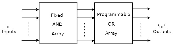
Here, the inputs of AND gates are not of programmable type. So, we have to generate 2n product terms by using 2n AND gates having n inputs each. We can implement these product terms by using nx2n decoder. So, this decoder generates n min terms.
Here, the inputs of OR gates are programmable. That means, we can program any number of required product terms, since all the outputs of AND gates are applied as inputs to each OR gate. Therefore, the outputs of PROM will be in the form of sum of min terms.
Example
Let us implement the following Boolean functions using PROM.
$$\mathrm{A(X,Y,Z)\:=\:\sum m\left ( 5,6,7 \right )}$$
$$\mathrm{B(X,Y,Z)\:=\:\sum m\left ( 3,5,6,7 \right )}$$
The given two functions are in sum of min terms form and each function is having three variables X, Y & Z. So, we require a 3 to 8 decoder and two programmable OR gates for producing these two functions. The corresponding PROM is shown in the following figure.

Here, 3 to 8 decoder generates eight min terms. The two programmable OR gates have the access of all these min terms. But, only the required min terms are programmed in order to produce the respective Boolean functions by each OR gate. The symbol X is used for programmable connections.
What is a Programmable Logic Device?
A Programmable Logic Device (PLD) can be defined as an integrated circuit (IC) which can be programmed to perform specific functions. Here, programming means we can define a set of instructions that can be executed to perform the functions multiple times without need of any human intervention.
The primary need of developing PLDs is occurred to implement digital logic functions that can copy the behavior of conventional logic circuits and replicate it many times. However, the PLDs are different from normal digital logic circuits in terms of programmability, which means we can define the desired logic functions by setting a collection of instructions in the device.
Types of PLDs
Based on the type of device used, Programmable Logic Devices (PLDs) can be classified into the following two types −
- Bipolar PLDs
- CMOS PLDs
Let us discuss each type of programmable logic device in detail.
Bipolar PLDs
Bipolar PLDs are the types of programmable logic devices in which Bipolar Junction Transistor (BJT) is the main functional device. Bipolar PLDs are the older versions of programmable logic devices. Thus, they were commonly used before the development of CMOS PLDs.
The following are some important characteristics of the bipolar programmable logic devices −
- Bipolar PLDs provide fast switching speeds and hence they can operate at higher frequencies.
- Bipolar PLDs are better suited for applications involving rapid signal processing and require fast response times.
- Bipolar PLDs require more power to operate.
- Bipolar PLDs have better immunity to electronic noise and interference.
All these characteristics make the bipolar programmable logic devices well-suited to use in the applications where high-speed operation and reliability are critical, such as aerospace, military, and telecommunications systems.
CMOS PLDs
CMOS PLDs stand for Complementary Metal Oxide Semiconductor Programmable Logic Devices. As their name implies, CMOS PLDs use the CMOS transistors i.e., NMOS (N-channel Metal Oxide Semiconductor) and PMOS (P-channel Metal Oxide Semiconductor) transistors as the fundamental component.
CMOS PLDs are basically the modern versions of PLDs and are widely used in modern digital systems due to their numerous advantages.
Some important characteristics of CMOS PLDs are described below −
- CMOS PLDs require very less amount of power to operate. Hence, this characteristic makes the CMOS PLDs well-suited to use in battery-power devices where energy efficiency is an important factor.
- CMOS PLDs are more reliable and robust. As they are designed to withstand against various environmental factors like high/low temperatures, voltage fluctuations, and different radiation interferences.
- CMOS PLDs are also excellent in terms of scalability.
CMOS PLDs are newer PLD devices and hence are very commonly used in various modern electronics devices like consumer electronics, medical equipment, industrial automation systems, automotive systems.
PLD Programming Languages
In the case of programmable logic devices (PLDs), several different types of Hardware Description Languages (HDLs) are used to program them. Using these PLD programming languages, engineers and designers can define the behavior and logical functionality of the PLD circuit.
Some of the most commonly used PLD programming languages are described here −
VHDL
VHDL stands for VHSIC Hardware Description Language. It is a standardized hardware description language used for modelling and simulating digital circuits and systems. Using VHDL, engineers and developers can specify the structure and functionality of the digital circuits. VHDL is a best suited programming language for both combinational and sequential circuits because of its concurrent and sequential descriptions support.
VHDL is one of the most widely used programming language for designing and verification of highly complex digital circuits and systems like PLDs, ASICs, FPGAs, and more.
Verilog
Verilog is also a Hardware Description Language (HDL) used for designing and programming of PLDs. Similar to VHDL, Verilog also supports the concurrent and sequential descriptions that empower engineers and designers to define the structure and behavior of digital circuits.
This programming language is most commonly used in semiconductor industries for designing and programming different kinds of digital systems.
PALASM
PALASM stands for Programmable Array Logic Assembler. It is another Hardware Description Language (HDL) and Assembler used for programming programmable logic devices (PLDs). In the case of PALASM, the behavior, logic function, and structure of PLDs are described using a textual language format. Thus, the developers have to write PALASM code to describe the desired logic functions and interconnections. After that these codes are assembled into a format which is suitable for programmable logic devices.
However, PALASM is an older hardware description language that was very commonly used in the 1980s and early 1990s for developing PLD-based logic circuits.
ABEL
ABEL stands for Advanced Boolean Expression Language. It is a high-level hardware description language developed for programming the Programmable Logic Devices (PLDs).
In ABEL, the logic equations, truth tables, and register transfer level design descriptions are specified using a clearly readable syntax. Then, the ABEL compiler translates all these design descriptions into a format suitable for programming the desired PLDs. ABEL was a very commonly used user-friendly hardware description language in the 1990s.
CUPL
CUPL stands for Compiler for Universal Programmable Logic. It is another Hardware Description Language (HDL) and Compiler used for programming different kinds of PLDs. In this programming language, the logic functions, truth tables, and sequential logic instructions are specified in the form of simple syntax.
This HDL language was also very popular in the 1990s and early 2000s and was used for designing PLD based logic circuits.
All these are some important programming languages used to design and program the programmable logic devices. The languages PALASM, ABEL, and CUPL are mainly in low-complexity devices. Whereas, VHDL and Verilog are used to program the modern highly-complex PLDs.
Advantages of Programmable Logic Devices
Programmable Logic Devices (PLDs) have numerous advantages that make them vital tools in the field of digital system design. Some of the important benefits of programmable logic devices are listed here −
- Programmable logic devices (PLDs) are easy to program and reprogram. Hence, they provide significant flexibility in terms of designing and implementation of a variety of logic functions.
- PLDs allow for designing custom logic circuits to fulfil the specific requirements of applications. This can be done by programming the internal logic circuits of the device.
- PLDs can be used in prototyping and testing of digital circuits which help in new product development at a faster rate. By speeding up the product development process, PLDs help to reduce the time and cost involved in hardware design.
- PLDs provide a fast and cost-effective way of developing medium to complex digital logic circuits and systems. PLDs help to develop simple, less expensive, and compact digital systems by integrating a large number of logic functions and components into a single device.
- PLDs also support modern processing techniques like parallel processing, pipeline processing, etc. This feature helps to achieve high performance by simultaneous execution of logic functions.
Limitations of Programmable Logic Devices
Programmable Logic Devices (PLDs) offer several advantages as discussed above, but they also have certain limitations. The following are some of the key limitations of programmable logic devices −
- A programmable logic device can be designed to support a finite number of logic functions and elements. Thus, the implementation of complex digital circuits may require multiple devices.
- A PLD typically has a fixed number of input/output (I/O) pins. This limitation can cause an issue in terms of connectivity and interfacing with external/peripheral devices.
- Programming a PLD requires knowledge of Hardware Description Languages (HDLs) and design tools. Sometimes PLDs can malfunction due to unintentional reprogramming or data corruption.
- PLDs do not have inherent support for complex arithmetic operations and other high-level programming operations that are used in general purpose processors. Therefore, developers have to implement such operations and functionalities through custom logic designs.
Applications of Programmable Logic Devices
Programmable Logic Devices (PLDs) are used in a wide range of applications across different fields and industries to design digital logic circuits and implement various logic functions. Some common applications of programmable logic devices are listed below −
- PLDs are widely used in embedded systems to perform different real-time operations like controlling, interfacing, and processing of data.
- In the field of digital signal processing, PLDs are used to design digital filters, develop modem algorithms, perform signal processing, etc.
- PLDs play an important role in communication systems, as they help in performing various operations like signal routing, data encryption and decryption, protocol conversion, and more.
- In the field of aerospace and defence, PLDs are employed for accomplishing various critical functions like flight control, operating radar systems, guiding missiles, encryption of confidential data and more.
- PLDs are also used in robotics and industrial automation to control and monitor the operations of machinery.
- In medical equipment, PLDs are used for automated high-speed data processing, real-time analysis of medical data, patient monitoring, etc.
Conclusion
In conclusion, a programmable logic device is a digital device that can be programmed or trained to perform a specific logic function. It is primarily used for automation and efficiency improvement purposes in various applications.
In this chapter, we explained the basics, types, advantages, limitations, and applications of PLDs. In the upcoming chapter, we will explore different kinds of programmable logic devices along with their features and characteristics.
Programmable Logic Array (PLA)
In this chapter, we will talk about Programmable Logic Array (PLA), its block diagram, and applications. The programmable logic array (PLA) is a type of programmable logic device (PLD). Historically, PLA is the first PLD device. It contains an array/matrix of AND and OR gates whose configuration is done as per the needs of applications.
In a PLA, a set of fusible links is used to establish or remove the contact of a literal in the AND operation or contact of a product term in the OR operation. Therefore, a PLA is a type of PLD that allows both AND matrix and OR matrix to program.
In digital electronics, PLAs are used to design and implement a variety of complex combinational circuits. However, some PLAs also have a memory element, hence they can be used to implement sequential circuits as well.
Block Diagram of PLA
A programmable logic array (PLA) is a type of fixed architecture programmable logic device (PLD) which consists of programmable AND and OR gates. A PLA contains a programmable AND array which is followed by a programmable OR array.
The block diagram of the PLA is shown in the following figure −
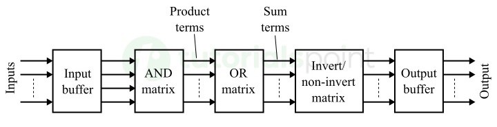
It consists of the following main components −
Input Buffer
The input buffer is used in PLA to avoid the loading effect on the source that drives the inputs.
AND Array/Matrix
The AND array/matrix is used in PLA to generate the product terms.
OR Array/Matrix
In a PLA, the OR array/matrix is used to generate the desired output. This is done by Oring the product terms to produce the sum terms.
Invert/Non-Invert Matrix
It is a buffer used in PLAs to set the output to active-high or active-low.
Output Buffer
This buffer is used at the output side. It is mainly provided to increase the driving capability of the programmable logic array (PLA).
Combinational Logic Design using PLA
In the field of digital electronics, the PLAs are extensively used for designing combinational logic circuits. The greatest advantage of designing combinational circuits using PLAs is that PLA consist of programmable AND and OR arrays which allows to implement custom desired logic functions.
The step-by-step procedure to design a combinational logic circuit using PLAs is explained below −
Step 1 − Develop a PLA program table that shows the inputs, product terms, and outputs.
Step 2 − Design the AND matrix that can generate the desired product terms.
Step 3 − Design the OR matrix that can generate the desired output.
Step 4 − Design the invert/non-invert matrix to set the active-low or active-high output.
Step 5 − Finally, program the PLA by utilizing the PLA program table.
Let us understand this process of combinational circuit design using PLA with the help of an example.
Example
Design a full-adder circuit using programmable logic array (PLA).
Solution
A full-adder consists of three-inputs and two outputs. Since it has 3 inputs, thus there are total 8 product terms which are given in the following truth table of the full adder −
| Inputs | Outputs | |||
|---|---|---|---|---|
| A | B | Cin | S | Cout |
| 0 | 0 | 0 | 0 | 0 |
| 0 | 0 | 1 | 1 | 0 |
| 0 | 1 | 0 | 1 | 0 |
| 0 | 1 | 1 | 0 | 1 |
| 1 | 0 | 0 | 1 | 0 |
| 1 | 0 | 1 | 0 | 1 |
| 1 | 1 | 0 | 0 | 1 |
| 1 | 1 | 1 | 1 | 1 |
From this truth table, the output sum (S) and the output carry (Cout) are given by,
$$\mathrm{S \: = \: \sum \: m(1,2,4,7)}$$
$$\mathrm{C_{out} \: = \: \sum \: m(3,5,6,7)}$$
Thus, their Boolean expressions will be,
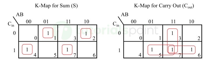
$$\mathrm{S \: = \: \overline{A} \: B \: \overline{C_{in}} \: + \: \overline{A} \: \overline{B} \: C_{in} \: + \: A \: \overline{B} \: \overline{C_{in}} \: + \: A \: B \: C_{in}}$$
$$\mathrm{C_{out} \: = \: A \: B \: + \: B \: C_{in} \: + \: A \: C_{in}}$$
From these two Boolean expressions, we can see that there are seven product terms and two sum terms. The PLA program table for this full-adder circuit is shown below −
| Sr.No | Product Terms | Inputs | Outputs | |||
|---|---|---|---|---|---|---|
| A | B | Cin | S | Cout | ||
| 1 | $\mathrm{\overline{A} \: B \: \overline{C_{in}}}$ | 0 | 1 | 0 | 1 | - |
| 2 | $\mathrm{\overline{A} \: \overline{B} \: C_{in}}$ | 0 | 0 | 1 | 1 | - |
| 3 | $\mathrm{A \: \overline{B} \: \overline{C_{in}}}$ | 1 | 0 | 0 | 1 | - |
| 4 | $\mathrm{A \: B \: C_{in}}$ | 1 | 1 | 1 | 1 | - |
| 5 | $\mathrm{A \: B }$ | 1 | 1 | - | - | 1 |
| 6 | $\mathrm{B \: C_{in}}$ | - | 1 | 1 | - | 1 |
| 7 | $\mathrm{A \: C_{in}}$ | 1 | - | 1 | - | 1 |
| T | T | |||||
In this PLA program table, "1" stands for the connection and "-" stands for the absence of the product term in the output. "T" stands for true and it represents the active-high output.
The PLA circuit diagram of the full-adder is shown in the following figure.
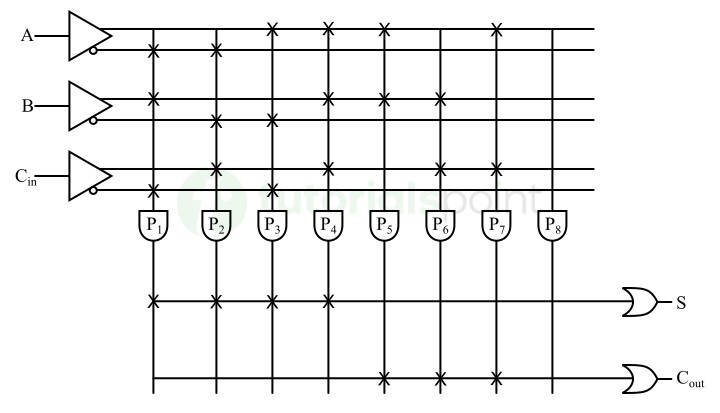
This example illustrates the complete step-by-step procedure to implement a combinational logic circuit using PLA.
Advantages of PLAs
The following are some key advantages of Programmable Logic Arrays (PLAs) that make them indispensable in the field of digital electronics −
- PLAs provide flexibility in terms of design and implementation of a variety of digital logic operations. PLAs can be used to implement custom logic functions required to fulfil the needs of different applications.
- PLAs also minimize the time required to design and develop a new digital circuit or system.
- PLAs provide a less expensive way of implementing highly complex digital logic functions. PLAs eliminate the need of discrete components to implement a logic function, hence they result in space efficiency.
- Since PLAs are programmable, they can be modified on their designs without re-fabricating the entire circuit.
Disadvantages of PLAs
However, PLAs offer several advantages as discussed above. But they also have some disadvantages which are listed below −
- For a large number of inputs and outputs, PLAs are highly complex to design and implement. Being a fixed architecture device, PLAs have limited performance in terms of speed and processing power.
- A PLA is generally optimized for a specific application, as it has a fixed number of AND gates and OR gates. This constraint disallows the designers to implement highly complex logic functions with the same PLA.
- Program a PLA is a time consuming and complex process.
Applications of PLAs
Programmable Logic Arrays (PLAs) are widely used in various applications across different fields. The following are some common applications of PLAs −
- PLAs are used in the field of digital signal processing to implement various logical functions, such as filtering, convolution, Fourier transformation, etc.
- In control systems, PLAs are used to implement control logic functions of various components like feedback, PID controllers, state machines, etc.
- PLAs are used to perform different types of arithmetic operations like addition, subtraction, multiplication, and division.
- PLAs also find their application in the field data compression and encryption technologies. PLAs are used in digital communication systems and networking equipment to implement algorithms for protocol handling, packet processing, error detection and correction, and more.
- PLAs are also used in different measuring instruments such as digital oscilloscopes, protocol analyzers, logic analyzer, etc.
Conclusion
A PLA is nothing but a kind of digital logic device used to implement complex digital functions without need of discrete components like AND gates, OR gates, etc. In this chapter, we explained the basics and applications of programmable logic arrays (PLAs).
Programmable Array Logic (PAL)
In the previous chapter, we explained Programmable Logic Array (PLA) which is a first programmable logic device (PLD). This chapter will deal with another type of programmable logic device called Programmable Array Logic (PAL).
The primary difference between PLA and PAL is that in a PLA device, both AND array and OR array are programmable, whereas in the case of PAL, the OR array is fixed while the AND array is programmable. A programmable array logic (PAL) also consists of arrays of AND and OR gates.
The most significant advantage that the PAL has is that it is very easy to program, as it contains only a programmable AND gate array, although it is not as flexible as the PLA.
What is a PAL?
In the field of digital electronics, there are several different types of programmable logic devices or PLDs. The Programmable Array Logic (PAL) is also a type of PLD used to design and implement a variety of custom logic functions. These programmable array logic devices allow digital designers to develop complex logic structures with high flexibility and efficiency.
Construction-wise, a PAL device consists of an array of programmable AND gates connected to a fixed array of OR gates. This array structure helps to implement various logic functions by interconnecting the input lines, AND gates and OR gates.
Block Diagram of PAL
Similar to PLA, the Programmable Array Logic (PAL) is also a type of fixed architecture logic device having an array of programmable AND gates and an array of fixed OR gates as shown in the following figure −
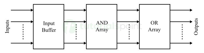
From this block diagram, it can be seen that a PAL consists of the following three main components −
- Input Buffers
- AND Gate Array
- OR Gate Array
These components are connected together through a programmed connection indicated by "X". In practice, these programmed connections can be made through EPROM cells or other programming technologies.
Combinational Logic Design Using PAL Devices
We can design combinational logic circuits using Programmable Array Logic (PAL) devices. While designing combinational logic using PAL, it is important to note that the Boolean expression in the sum products form must be simplified to fit into each section of the PAL.
Because the array of OR gates is fixed, the number of product terms fed to each OR gate cannot be changed. If there is a situation when the number of product terms are more, then the Boolean function must be implemented for that section.
Let us understand the combinational logic design using PAL devices with the help of examples.
Example
Consider a combinational logic circuit which has 3 inputs and 2 outputs. The logic functions for the outputs are given below. Implement this circuit using PAL.
$$\mathrm{X(A,B,C) \: = \: \sum \: m(1,2,4,6)}$$
$$\mathrm{Y(A,B,C) \: = \: \sum \: m(0,1,3,6,7)}$$
Solution
Obtaining the Boolean expressions for the given logic functions,

From these K-maps, we get,
$$\mathrm{X \: = \: A\overline{C} \: + \: B\overline{C} \: + \: \overline{A} \: \overline{B} C}$$
$$\mathrm{Y \: = \: \overline{A} \:\overline{B} \: + \: BC \: + \: AB}$$
Now, prepare the PAL program table for these output functions, which is given below −
| Product Terms | AND Gate Inputs | |||
|---|---|---|---|---|
| A | B | C | ||
| 1 | $\mathrm{A \: \overline{B}}$ | 1 | - | 0 |
| 2 | $\mathrm{B \: \overline{C}}$ | - | 1 | 0 |
| 3 | $\mathrm{\overline{A} \: \overline{B} \: C}$ | 0 | 0 | 1 |
| 4 | $\mathrm{\overline{A} \: \overline{B}}$ | 0 | 0 | - |
| 5 | $\mathrm{B \: C}$ | - | 1 | 1 |
| 6 | $\mathrm{A \: B}$ | 1 | 1 | - |
Now, let's implement the PAL logic circuit as per this table. This circuit diagram is shown in the following figure −
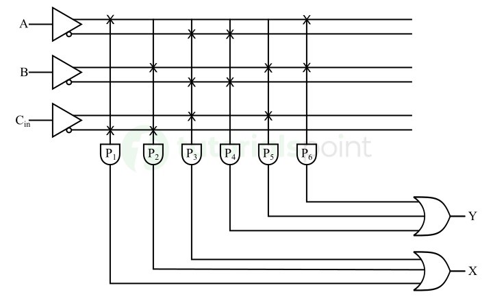
This is how we can implement a logic function using Programmable Array Logic (PAL).
Advantages of PAL
In the field of digital electronics, Programmable Array Logic (PAL) is widely used in combinational and sequential circuit designing due to the several advantages it offers.
- PAL devices provide greater flexibility in design and implementation of custom logic functions, as it can be programmed by making interconnections between the input lines and the AND gates so that it can meet the requirements of a specific application.
- PAL devices also provide less expensive ways of implementing complex logic functions. This is because PALs eliminate the requirement of custom fabrication processes due to its ability to program.
- PALs also help to minimize the time required for developing and launching the electronic products.
- Due to their high integration density, PALs allow for implementing multiple logic functions within a single device. Consequently, they help in developing compact and efficient designs.
Disadvantages of PAL
However, Programmable Array Logics (PALs) have several advantages as given above, but they also have some disadvantages as listed below −
- PAL devices have some limitations in terms of complexity in the implementation of logic functions. This is because, a PAL contains a certain number of input lines, AND gates, and OR gates. Thus, if we need to implement a complex logic function, then we can require multiple PALs.
- PAL devices have a fixed architecture which contains an array of fixed OR gates and an array of programmable AND gates. Therefore, these devices cannot be used to implement certain logic functions.
- Since PALs have a finite number of input and output lines. This results in a limit in terms of the I/O connectivity of the electronic device.
- It is very complex and time-consuming process to program a PAL device. It also requires some specialized tools and expertise.
Applications of PAL
Programmable Array Logics (PALs) are extensively used in a variety of applications in the field of digital electronics. Some common applications of PALs are listed below −
- PALs are used in embedded systems for implementing control logics, providing interfacing between different components, sensors, and other subsystems, and performing various signal processing tasks like filtering, modulation, demodulation, signal conditioning, etc.
- In communication systems, PALs are employed for implementing encoding and decoding algorithms, protocol processing, error detection and correction, multiplexing and demultiplexing, etc.
- PALs are also used in the field of automotive electronics for implementing control logics for managing engine functions, fuel injection, emission control system, anti-lock braking system, audio system, navigation, and driver assistance system.
- In industrial automation and robotics, the PALs play an important role, as they help to develop logic functions for controlling and monitoring industrial processes, sensors, and other components.
- PALs are also used in consumer electronics like washing machines, microwave ovens, home automation systems, etc. to implement their control functions.
Conclusion
A PAL is a type of programmable logic device used to implement combinational and sequential logics and is used as a versatile device across a wide range of fields.
Due to its greater flexibility, easy programmability, and reliability, PAL has become an important tool in the field of digital electronics.
Field Programmable Gate Arrays (FPGAs)
What is a Field-Programmable Gate Array
A Field-Programmable Gate Array (FPGA) is a type of programmable logic device (PLD) that provides high degree of flexibility and can be used for implementing complete digital system on a single chip. It contains an array of identical logic cells that can be programmed. By programming these logic cells or blocks, FPGAs can be used to perform various logic functions. Also, we can interconnect them to implement complex digital systems.
FPGAs also have several input/output (I/O) blocks to create interface between external devices and the FPGAs internal logic circuit. They also consist of a memory element to store the programs that specifies the operational behavior of the logic cells and programmable interconnects.
In order to program FPGAs, there are various hardware description languages (HDLs) available like Verilog or VHDL. These programming languages are used to define the desired functionality and behavior of the digital system.
The general block diagram of an FPGA is depicted in the following figure.

Components of FPGA
It consists of the following main components −
- Configurable Logic Blocks (CLBs)
- I/O Blocks
- Programmable Interconnects
The configurable logic block consists of multiplexers, flip-flops, and array of combination logic circuits. Th I/O blocks provide pins to connect external devices with the FPGA. The programmable interconnect is basically a switching matrix structure that provides interconnection between CLB and I/O blocks inside the FPGA.
Certainly! The classification of FPGAs into low-end, mid-range, and high-end categories is based on their performance, complexity, gate density, and power consumption. Let's delve deeper into each category −
Types of FPGAs
Depending on the applications, FPGAs can be classified into the following main types −
- Low-End FPGAs
- Mid-Range FPGAs
- High-End FPGAs
Let us now discuss these different types of FPGAs in detail.
Low-End FPGAs
Low-End FPGAs are primarily designed to consume least power than the mid-range and high-end FPGAs. Thus, they are well-suited to use in battery-powered devices and other applications where energy efficiency is critical.
In low-end FPGAs, a smaller number of logic gates are used, hence they use less resources for implementing complex logic systems. Also, these FPGAs have a less complex architecture. Some common applications of low-end FPGAs include simple control systems, basic signal processing systems, and low-cost consumer electronics.
Mid-Range FPGAs
Mid-range FPGAs take more power than low-end FPGAs but less power than high-end FPGAs. This is mainly because the mid-range FPGAs consist of a larger number of logic gates as compared to low-end FPGAs. This in turn increases the overall complexity of the circuit. Although, these FPGAs offer a balance between performance and efficiency.
Since mid-range FPGAs provide a larger number of resources, they allow to implement more complex digital circuits.
These FPGAs are used in a wide range of applications such as digital signal processing, communication systems, embedded systems, industrial automation systems, telecommunication devices, medical equipment, etc.
High-End FPGAs
High-end FPGAs consume more power than both low-end and mid-range FPGAs. This is because they use a larger number of logic gates and also have higher operating frequencies. Although, these FPGAs are supposed to be exceptional in terms of performance and processing efficiency.
Due to availability of large number resources, the high-end FPGAs can be used for implementing highly complex logic circuits and systems. Also, they provide the highest level of flexibility and performance.
Some common applications where the high-end FPGAs are used include high-speed processing systems, real-time data analysis systems, data centers, high-performance computing systems, aerospace and defense systems, etc.
Advantages of FPGAs
FPGAs offer numerous advantages over other types of programmable logic devices. Some of the major advantages of FPGAs are listed below −
- FPGAs provide a greater flexibility and re-configurability, as they can be programmed or reprogrammed to implement different logic functions to meet the requirements of specific applications without need of hardware alteration or redesign.
- FPGAs allow to develop digital systems in less time.
- FPGAs have high performance and processing capabilities. Hence, they can execute complex algorithms and tasks more efficiently.
- FPGAs can be customized and optimized to meet the requirements of specific applications.
- FPGAs also support parallelism and pipelining. These technologies allow to enhance the overall system performance and throughput.
Disadvantages of FPGAs
FPGAs offer several advantages as listed above, but they also have certain disadvantages. Some of the main disadvantages of FPGAs are highlighted here −
- FPGAs are more expensive than other types of programmable logic devices.
- FPGAs are complex to design and implement and require more time and expertise in hardware description languages (HDLs) and system design tools.
- FPGAs are more susceptible to security threats than other types of programmable logic devices.
Applications of FPGAs
FPGAs are extensively used in several applications across a wide range of industries. The following are some common applications of FPGAs −
- FPGAs are used in the field of digital signal processing to accomplish tasks such as audio-video signal processing, speech recognition, image processing, etc.
- FPGAs are used in the implementation of complex algorithms and real-time signal processing functions.
- FPGAs are used in various communication and networking devices such as routers, switches, network processing units, etc.
- In communication systems, FPGAs are employed for implementing protocol processing algorithms, packet handling algorithms, encryption-decryption techniques, error detection and correction mechanisms, etc.
- FPGAs are used in a variety of electronic systems such as embedded systems, industrial automation systems, automotive electronics, consumer electronic devices, etc.
- FPGAs are used to perform high-end processing tasks such as scientific computation, data analysis, machine learning and artificial intelligence tasks.
- FPGAs are also integral parts in various medical equipment such as MRI (Magnetic Resonance Imaging), CT (Computed Tomography) scan, ultrasound systems, X-ray machines, etc.
Conclusion
In conclusion, FPGAs are programmable logic devices used in implementing a complex digital system in the form of a single integrated circuit chip. Due to their high performance and computing capabilities, they are used in a diverse range of applications across various industries.
Digital Electronics - Families
A logic family is defined as a set of electronic circuit designs that have similar characteristics in terms of technical parameters such as logic levels, voltage levels, switching speed, power consumption, noise immunity, etc. The logic families play an important role in the field of digital electronics and allows to implement various logic functions and operations.
Depending on the fabrication technology, the logic families can be classified into the following two types −
- Unipolar Logic Family
- Bipolar Logic Family
A logic family that utilizes unipolar electronic devices like MOSFETs as their main element is known as a unipolar logic family. Some examples of unipolar logic families include PMOS, NMOS, and CMOS.
On the other hand, a bipolar logic family is one that utilizes bipolar electronic devices such as transistors and diodes. The bipolar logic families can be further classified into the following types −
- Resistor-Transistor Logic (RTL)
- Diode Transistor Logic (DTL)
- Transistor-Transistor Logic (TTL)
Let us now discuss about each of these logic families in detail.
Resistor-Transistor Logic (RTL)
As the name implies, this logic family utilizes resistors and transistors as their key elements. In the RTL family, the transistors operate in the cut-off or saturation regions depending on the input voltage applied to them. The RTL family was one of the earliest logic families used in the field of digital electronic design.
In short, in the RTL family, the logic circuits are designed using resistors and transistors only.
For example, the circuit of a two-input resistor-transistor logic NOR gate is shown in the following figure. Here, A and B are the inputs and Y is the output of the gate.
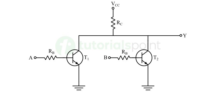
The operation of this RTL NOR gate for different input combinations is highlighted in the following table −
| Input A | Input B | Transistor T1 | Transistor T2 | Output Y |
|---|---|---|---|---|
| 0 | 0 | Off | Off | 1 |
| 0 | 1 | Off | On | 0 |
| 1 | 0 | On | Off | 0 |
| 1 | 1 | On | On | 0 |
Similarly, we can also implement other types of logic gates as well.
Advantages of RTL Family
The following are some key advantages of resistor-transistor logic family −
- Electronic circuits designed using RTL logic family are simple in design, as they consist of a minimum number of resistors and transistors.
- Circuits manufactured in RTL family are less expensive. These circuits consume less amount of power than circuits implemented in other logic families.
Disadvantages of RTL Family
The following are some major drawbacks of resistor-transistor logic families −
- RTL circuits have low noise margin. This limitation makes them susceptible to noise and interference.
- These circuits have poor fan-out.
- RTL circuits are slower in operation due to high propagation delay.
- RTL family is not suitable for designing complex circuits due to some practical limitations in terms of design scalability and performance.
Applications of RTL Family
Resistor-Transistor Logic (RTL) family finds some limited applications in the field of digital electronics. Some common applications of RTL family are listed below −
- RTL family is cost-effective and easy to understand and design. For this reason, it is widely used for educational purposes in labs and classrooms to demonstrate digital electronic concepts to students.
- RTL family is also used to design circuits for low-frequency control applications. Due to simplicity and ease of implementation, RTL family can be used for prototyping and experimental purposes.
Diode Transistor Logic (DTL)
In diode-transistor logic (DTL) family, the diodes and transistors are the key elements combinedly used to implement digital logic functions.
The following example circuit demonstrates the electronic circuit design in DTL family.

It is a two-input NAND gate. Where, A and B are inputs of the NAND gate and Y is the output of the gate.
The operation of this two-input NAND gate is explained in the following truth table −
| Input A | Input B | Diode D1 | Diode D2 | Transistor T | Output Y |
|---|---|---|---|---|---|
| 0 | 0 | Forward biased | Forward biased | Off | 1 |
| 0 | 1 | Forward biased | Reverse biased | Off | 1 |
| 1 | 0 | Reverse biased | Forward biased | Off | 1 |
| 1 | 1 | Reverse biased | Reverse biased | On | 0 |
We can also implement other types of logic circuits using the diode-transistor logic family.
Advantages of DTL Family
The following are some key advantages of diode-transistor logic family −
- DTL circuits are easy and simple to design and implement, as they consist of only diodes, transistors, and resistors.
- DTL circuits are cost-effective as they use basic electronic components like diodes and transistors which are generally cheap.
- DTL circuits have good noise immunity. Hence, these circuits are relatively less susceptible to noise and interference than some other types of logic families.
- DTL circuits have high fan-out. The power dissipation in DTL circuits is comparatively low.
Limitations of DTL Family
Apart from the advantages given above, the DTL circuits also have some disadvantages which are listed below −
- DTL family circuits require higher amount of power as compared to other logic families.
- DTL circuits consist of a greater number of elements than other types of logic families.
- DTL circuits have a moderate speed of operation. This is due to high propagation delay.
- DTL circuits are not suitable to design more complex digital circuits due to increased complexity and size of the circuit.
Applications of DTL Family
The following are some common applications of diode-transistor logic family −
- DTL family was popular in early digital computers and other digital systems.
- These days, DTL circuits are mainly used for educational purposes to explain the implementation of digital logic designs to students.
- DTL circuits are used to design custom electronic projects.
Transistor-Transistor Logic (TTL)
Transistor-Transistor Logic (TTL) is one of the most popular logic family in the field of digital electronics. In this logic family, the transistor is the key functional element which is operated as a switch to perform the logical operations.
Let us now understand how we can design a logic circuit in TTL family. The following figure shows a two-input NAND gate −

Here, A and B are the input terminals and Y is the output terminal. The operation of this circuit is summarized in the following table.
| Input A | Input B | Emitter Junction of Transistor T1 | Emitter Junction of Transistor T2 | Transistor T2 and T3 | Output Y |
|---|---|---|---|---|---|
| 0 | 0 | Forward biased | Forward biased | Off | 1 |
| 0 | 1 | Forward biased | Reverse biased | Off | 1 |
| 1 | 0 | Reverse biased | Forward biased | Off | 1 |
| 1 | 1 | Reverse biased | Reverse biased | On | 0 |
In the same manner, we can also design other logic gates in the transistor-transistor logic (TTL) family.
Advantages of TTL Family
Here are some of the key advantages of TTL family −
- TTL circuits have high speeds of operation and hence well-suited to use in high-speed digital systems.
- TTL circuits are standardized to make them compatible with a variety of digital circuits and systems.
- TTL circuits have good noise immunity. Thus, they are suitable to use in noisy environments.
Disadvantages of TTL Family
Although, TTL circuits have several advantages as listed above. But they also have some disadvantages which are given below −
- TTL circuits consume more power than other types of logic families. This limitation makes the TTL circuits less energy efficient.
- TTL circuits generate significant heat during operation and this is due to high power consumption. Thus, a proper heat management system is required.
- TTL logic levels are relatively strict, requiring specific voltage levels for proper operation. This can sometimes lead to compatibility issues with other logic families.
- TTL circuits have a significant propagation delay that limit their use in certain high-speed systems.
Applications of TTL Family
Transistor-Transistor Logic (TTL) family are widely used in various applications in the field of digital electronics. Some of the common applications of TTL family are listed below −
- TTL circuits are widely used in digital computers, memory units, CPUs, etc.
- TTL circuits are also used in embedded systems for different purposes such as interfacing with sensors, processing data in real-time applications, and more.
- In communication systems, TTL circuits are for signal conditioning, protocol handling, data processing, etc. TTL circuits are commonly used in a variety of testing and measuring instruments.
Conclusion
In conclusion, a logic family is a set of digital circuits that share same technical parameters such as logic levels, voltage levels, processing speed, etc. In this chapter, we explained the most commonly used digital logic families viz. RTL, DTL, and TTL, along with their advantages, disadvantages, and applications.
CPU Architecture
Microprocessing unit is synonymous to central processing unit, CPU used in traditional computer. Microprocessor (MPU) acts as a device or a group of devices which do the following tasks.
- Communicate with peripherals devices
- Provide timing signal
- Direct data flow
- Perform computer tasks as specified by the instructions in memory
8085 Microprocessor
The 8085 microprocessor is an 8-bit general purpose microprocessor which is capable to address 64k of memory. This processor has forty pins, requires +5 V single power supply and a 3-MHz single-phase clock.
Block Diagram

ALU
The ALU perform the computing function of microprocessor. It includes the accumulator, temporary register, arithmetic & logic circuit & and five flags. Result is stored in accumulator & flags.
Block Diagram
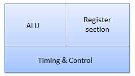
Accumulator
It is an 8-bit register that is part of ALU. This register is used to store 8-bit data & in performing arithmetic & logic operation. The result of operation is stored in accumulator.
Diagram
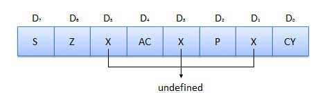
Flags
Flags are programmable. They can be used to store and transfer the data from the registers by using instruction. The ALU includes five flip-flops that are set and reset according to data condition in accumulator and other registers.
- S (Sign) flag − After the execution of an arithmetic operation, if bit D7 of the result is 1, the sign flag is set. It is used to signed number. In a given byte, if D7 is 1 means negative number. If it is zero means it is a positive number.
- Z (Zero) flag − The zero flag is set if ALU operation result is 0.
- AC (Auxiliary Carry) flag − In arithmetic operation, when carry is generated by digit D3 and passed on to digit D4, the AC flag is set. This flag is used only internally BCD operation.
- P (Parity) flag − After arithmetic or logic operation, if result has even number of 1s, the flag is set. If it has odd number of 1s, flag is reset.
- C (Carry) flag − If arithmetic operation result is in a carry, the carry flag is set, otherwise it is reset.
Register Section
It is basically a storage device and transfers data from registers by using instructions.
- Stack Pointer (SP) − The stack pointer is also a 16-bit register which is used as a memory pointer. It points to a memory location in Read/Write memory known as stack. In between execution of program, sometime data to be stored in stack. The beginning of the stack is defined by loading a 16-bit address in the stack pointer.
- Program Counter (PC) − This 16-bit register deals with fourth operation to sequence the execution of instruction. This register is also a memory pointer. Memory location have 16-bit address. It is used to store the execution address. The function of the program counter is to point to memory address from which next byte is to be fetched.
- Storage registers − These registers store 8-bit data during a program execution. These registers are identified as B, C, D, E, H, L. They can be combined as register pair BC, DE and HL to perform some 16 bit operations.
Time and Control Section
This unit is responsible to synchronize Microprocessor operation as per the clock pulse and to generate the control signals which are necessary for smooth communication between Microprocessor and peripherals devices. The RD bar and WR bar signals are synchronous pulses which indicates whether data is available on the data bus or not. The control unit is responsible to control the flow of data between microprocessor, memory and peripheral devices.
PIN Diagram
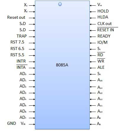
All the signal can be classified into six groups
| Sr.No | Group | Description |
|---|---|---|
| 1 | Address bus | The 8085 microprocessor has 8 signal line, A15 - A8 which are uni directional and used as a high order address bus. |
| 2 | Data bus | The signal line AD7 - AD0 are bi-directional for dual purpose. They are used as low order address bus as well as data bus. |
| 3 | Control signal and Status signal |
Control Signal RD bar − It is a read control signal (active low). If it is active then memory read the data. WR bar − It is write control signal (active low). It is active when written into selected memory. Status signal ALE (Address Latch Enable) − When ALE is high. 8085 microprocessor use address bus. When ALE is low. 8085 microprocessor is use data bus. IO/M bar − This is a status signal used to differentiate between i/o and memory operations. When it is high, it indicate an i/o operation and when it is low, it indicate memory operation. S1 and S0 − These status signals, similar to i/o and memory bar, can identify various operations, but they are rarely used in small system. |
| 4 | Power supply and frequency signal |
Vcc − +5v power supply. Vss − ground reference. X, X − A crystal is connected at these two pins. The frequency is internally divided by two operate system at 3-MHz, the crystal should have a frequency of 6-MHz. CLK out − This signal can be used as the system clock for other devices. |
| 5 | Externally initiated signal |
INTR (i/p) − Interrupt request. INTA bar (o/p) − It is used as acknowledge interrupt. TRAP (i/p) − This is non maskable interrupt and has highest priority. HOLD (i/p) − It is used to hold the executing program. HLDA (o/p) − Hold acknowledge. READY (i/p) − This signal is used to delay the microprocessor read or write cycle until a slow responding peripheral is ready to accept or send data. RESET IN bar − When the signal on this pin goes low, the program counter is set to zero, the bus are tri-stated, & MPU is reset. RESET OUT − This signal indicate that MPU is being reset. The signal can be used to reset other devices. RST 7.5, RST 6.5, RST 5.5 (Request interrupt) − It is used to transfer the program control to specific memory location. They have higher priority than INTR interrupt. |
| 6 | Serial I/O ports | The 8085 microprocessor has two signals to implement the serial transmission serial input data and serial output data. |
Instruction Format
Each instruction is represented by a sequence of bits within the computer. The instruction is divided into group of bits called field. The way instruction is expressed is known as instruction format. It is usually represented in the form of rectangular box. The instruction format may be of the following types.
Variable Instruction Formats
These are the instruction formats in which the instruction length varies on the basis of opcode & address specifiers. For Example, VAX instruction vary between 1 and 53 bytes while X86 instruction vary between 1 and 17 bytes.
Format

Advantage
These formats have good code density.
Drawback
These instruction formats are very difficult to decode and pipeline.
Fixed Instruction Formats
In this type of instruction format, all instructions are of same size. For Example, MIPS, Power PC, Alpha, ARM.
Format
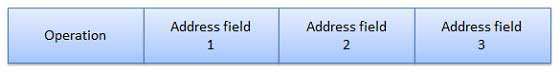
Advantage
They are easy to decode & pipeline.
Drawback
They don't have good code density.
Hybrid Instruction Formats
In this type of instruction formats, we have multiple format length specified by opcode. For example, IBM 360/70, MIPS 16, Thumb.
Format
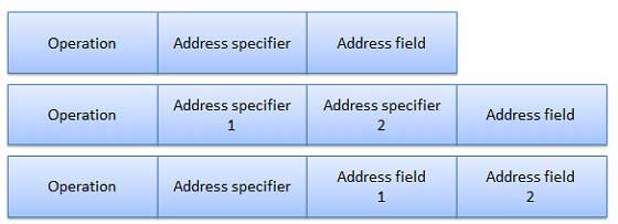
Advantage
These compromise between code density & instruction of these type are very easy to decode.
Addressing Modes
Addressing mode provides different ways for accessing an address to given data to a processor. Operated data is stored in the memory location, each instruction required certain data on which it has to operate. There are various techniques to specify address of data. These techniques are called Addressing Modes.
- Direct Addressing Mode − In the direct addressing mode, address of the operand is given in the instruction and data is available in the memory location which is provided in instruction. We will move this data in desired location.
- Indirect Addressing Mode − In the indirect addressing mode, the instruction specifies a register which contain the address of the operand. Both internal RAM and external RAM can be accessed via indirect addressing mode.
- Immediate addressing Mode − In the immediate addressing mode, direct data is given in the operand which move the data in accumulator. It is very fast.
- Relative Addressing Mode − In the relative address mode, the effective address is determined by the index mode by using the program counter in stead of general purpose processor register. This mode is called relative address mode.
- Index Addressing Mode − In the index address mode, the effective address of the operand is generated by adding a content value to the contents of the register. This mode is called index address mode.
