- Digital Electronics - Home
- Digital Electronics Basics
- Types of Digital Systems
- Types of Signals
- Logic Levels And Pulse Waveforms
- Digital System Components
- Digital Logic Operations
- Digital Systems Advantages
- Number Systems
- Number Systems
- Binary Numbers Representation
- Binary Arithmetic
- Signed Binary Arithmetic
- Octal Arithmetic
- Hexadecimal Arithmetic
- Complement Arithmetic
- Base Conversions
- Base Conversions
- Binary to Decimal Conversion
- Decimal to Binary Conversion
- Binary to Octal Conversion
- Octal to Binary Conversion
- Octal to Decimal Conversion
- Decimal to Octal Conversion
- Hexadecimal to Binary Conversion
- Binary to Hexadecimal Conversion
- Hexadecimal to Decimal Conversion
- Decimal to Hexadecimal Conversion
- Octal to Hexadecimal Conversion
- Hexadecimal to Octal Conversion
- Binary Codes
- Binary Codes
- 8421 BCD Code
- Excess-3 Code
- Gray Code
- ASCII Codes
- EBCDIC Code
- Code Conversion
- Error Detection & Correction Codes
- Logic Gates
- Logic Gates
- AND Gate
- OR Gate
- NOT Gate
- Universal Gates
- XOR Gate
- XNOR Gate
- CMOS Logic Gate
- OR Gate Using Diode Resistor Logic
- AND Gate vs OR Gate
- Two Level Logic Realization
- Threshold Logic
- Boolean Algebra
- Boolean Algebra
- Laws of Boolean Algebra
- Boolean Functions
- DeMorgan's Theorem
- SOP and POS Form
- POS to Standard POS Form
- Minimization Techniques
- K-Map Minimization
- Three Variable K-Map
- Four Variable K-Map
- Five Variable K-Map
- Six Variable K-Map
- Don't Care Condition
- Quine-McCluskey Method
- Min Terms and Max Terms
- Canonical and Standard Form
- Max Term Representation
- Simplification using Boolean Algebra
- Combinational Logic Circuits
- Digital Combinational Circuits
- Digital Arithmetic Circuits
- Multiplexers
- Multiplexer Design Procedure
- Mux Universal Gate
- 2-Variable Function Using 4:1 Mux
- 3-Variable Function Using 8:1 Mux
- Demultiplexers
- Mux vs Demux
- Parity Bit Generator and Checker
- Comparators
- Encoders
- Keyboard Encoders
- Priority Encoders
- Decoders
- Arithmetic Logic Unit
- 7-Segment LED Display
- Code Converters
- Code Converters
- Binary to Decimal Converter
- Decimal to BCD Converter
- BCD to Decimal Converter
- Binary to Gray Code Converter
- Gray Code to Binary Converter
- BCD to Excess-3 Converter
- Excess-3 to BCD Converter
- Adders
- Half Adders
- Full Adders
- Serial Adders
- Parallel Adders
- Full Adder using Half Adder
- Half Adder vs Full Adder
- Full Adder with NAND Gates
- Half Adder with NAND Gates
- Binary Adder-Subtractor
- Subtractors
- Half Subtractors
- Full Subtractors
- Parallel Subtractors
- Full Subtractor using 2 Half Subtractors
- Half Subtractor using NAND Gates
- Sequential Logic Circuits
- Digital Sequential Circuits
- Clock Signal and Triggering
- Latches
- Shift Registers
- Shift Register Applications
- Binary Registers
- Bidirectional Shift Register
- Counters
- Binary Counters
- Non-binary Counter
- Design of Synchronous Counter
- Synchronous vs Asynchronous Counter
- Finite State Machines
- Algorithmic State Machines
- Flip Flops
- Flip-Flops
- Conversion of Flip-Flops
- D Flip-Flops
- JK Flip-Flops
- T Flip-Flops
- SR Flip-Flops
- Clocked SR Flip-Flop
- Unclocked SR Flip-Flop
- Clocked JK Flip-Flop
- JK to T Flip-Flop
- SR to JK Flip-Flop
- Triggering Methods:Flip-Flop
- Edge-Triggered Flip-Flop
- Master-Slave JK Flip-Flop
- Race-around Condition
- A/D and D/A Converters
- Analog-to-Digital Converter
- Digital-to-Analog Converter
- DAC and ADC ICs
- Realization of Logic Gates
- NOT Gate from NAND Gate
- OR Gate from NAND Gate
- AND Gate from NAND Gate
- NOR Gate from NAND Gate
- XOR Gate from NAND Gate
- XNOR Gate from NAND Gate
- NOT Gate from NOR Gate
- OR Gate from NOR Gate
- AND Gate from NOR Gate
- NAND Gate from NOR Gate
- XOR Gate from NOR Gate
- XNOR Gate from NOR Gate
- NAND/NOR Gate using CMOS
- Full Subtractor using NAND Gate
- AND Gate Using 2:1 MUX
- OR Gate Using 2:1 MUX
- NOT Gate Using 2:1 MUX
- Memory Devices
- Memory Devices
- RAM and ROM
- Cache Memory Design
- Programmable Logic Devices
- Programmable Logic Devices
- Programmable Logic Array
- Programmable Array Logic
- Field Programmable Gate Arrays
- Digital Electronics Families
- Digital Electronics Families
- CPU Architecture
- CPU Architecture
Programmable Logic Devices
Programmable Logic Devices (PLDs) are a collection of integrated circuits which are configured to perform various logical functions. PLDs play an important role in the field of engineering and technology, as they form the basis of innovation and support engineers to develop automated digital systems to improve process flexibility and efficiency. Here, "programmable" means defining a function that can be performed multiple times without human intervention.
Programmable Logic Devices (PLDs) are the integrated circuits. They contain an array of AND gates & another array of OR gates. There are three kinds of PLDs based on the type of array(s), which has programmable feature.
- Programmable Read Only Memory
- Programmable Array Logic
- Programmable Logic Array
The process of entering the information into these devices is known as programming. Basically, users can program these devices or ICs electrically in order to implement the Boolean functions based on the requirement. Here, the term programming refers to hardware programming but not software programming.
In this chapter, we will explain the basic concepts of programmable logic devices, their types, advantages, limitations, and applications.
Programmable Read Only Memory (PROM)
Read Only Memory (ROM) is a memory device, which stores the binary information permanently. That means, we cant change that stored information by any means later. If the ROM has programmable feature, then it is called as Programmable ROM (PROM). The user has the flexibility to program the binary information electrically once by using PROM programmer.
PROM is a programmable logic device that has fixed AND array & Programmable OR array. The block diagram of PROM is shown in the following figure.
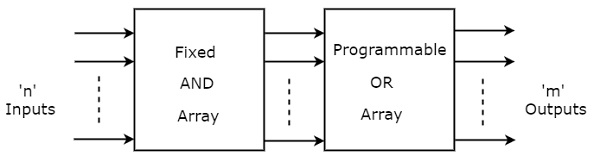
Here, the inputs of AND gates are not of programmable type. So, we have to generate 2n product terms by using 2n AND gates having n inputs each. We can implement these product terms by using nx2n decoder. So, this decoder generates n min terms.
Here, the inputs of OR gates are programmable. That means, we can program any number of required product terms, since all the outputs of AND gates are applied as inputs to each OR gate. Therefore, the outputs of PROM will be in the form of sum of min terms.
Example
Let us implement the following Boolean functions using PROM.
$$\mathrm{A(X,Y,Z)\:=\:\sum m\left ( 5,6,7 \right )}$$
$$\mathrm{B(X,Y,Z)\:=\:\sum m\left ( 3,5,6,7 \right )}$$
The given two functions are in sum of min terms form and each function is having three variables X, Y & Z. So, we require a 3 to 8 decoder and two programmable OR gates for producing these two functions. The corresponding PROM is shown in the following figure.

Here, 3 to 8 decoder generates eight min terms. The two programmable OR gates have the access of all these min terms. But, only the required min terms are programmed in order to produce the respective Boolean functions by each OR gate. The symbol X is used for programmable connections.
What is a Programmable Logic Device?
A Programmable Logic Device (PLD) can be defined as an integrated circuit (IC) which can be programmed to perform specific functions. Here, programming means we can define a set of instructions that can be executed to perform the functions multiple times without need of any human intervention.
The primary need of developing PLDs is occurred to implement digital logic functions that can copy the behavior of conventional logic circuits and replicate it many times. However, the PLDs are different from normal digital logic circuits in terms of programmability, which means we can define the desired logic functions by setting a collection of instructions in the device.
Types of PLDs
Based on the type of device used, Programmable Logic Devices (PLDs) can be classified into the following two types −
- Bipolar PLDs
- CMOS PLDs
Let us discuss each type of programmable logic device in detail.
Bipolar PLDs
Bipolar PLDs are the types of programmable logic devices in which Bipolar Junction Transistor (BJT) is the main functional device. Bipolar PLDs are the older versions of programmable logic devices. Thus, they were commonly used before the development of CMOS PLDs.
The following are some important characteristics of the bipolar programmable logic devices −
- Bipolar PLDs provide fast switching speeds and hence they can operate at higher frequencies.
- Bipolar PLDs are better suited for applications involving rapid signal processing and require fast response times.
- Bipolar PLDs require more power to operate.
- Bipolar PLDs have better immunity to electronic noise and interference.
All these characteristics make the bipolar programmable logic devices well-suited to use in the applications where high-speed operation and reliability are critical, such as aerospace, military, and telecommunications systems.
CMOS PLDs
CMOS PLDs stand for Complementary Metal Oxide Semiconductor Programmable Logic Devices. As their name implies, CMOS PLDs use the CMOS transistors i.e., NMOS (N-channel Metal Oxide Semiconductor) and PMOS (P-channel Metal Oxide Semiconductor) transistors as the fundamental component.
CMOS PLDs are basically the modern versions of PLDs and are widely used in modern digital systems due to their numerous advantages.
Some important characteristics of CMOS PLDs are described below −
- CMOS PLDs require very less amount of power to operate. Hence, this characteristic makes the CMOS PLDs well-suited to use in battery-power devices where energy efficiency is an important factor.
- CMOS PLDs are more reliable and robust. As they are designed to withstand against various environmental factors like high/low temperatures, voltage fluctuations, and different radiation interferences.
- CMOS PLDs are also excellent in terms of scalability.
CMOS PLDs are newer PLD devices and hence are very commonly used in various modern electronics devices like consumer electronics, medical equipment, industrial automation systems, automotive systems.
PLD Programming Languages
In the case of programmable logic devices (PLDs), several different types of Hardware Description Languages (HDLs) are used to program them. Using these PLD programming languages, engineers and designers can define the behavior and logical functionality of the PLD circuit.
Some of the most commonly used PLD programming languages are described here −
VHDL
VHDL stands for VHSIC Hardware Description Language. It is a standardized hardware description language used for modelling and simulating digital circuits and systems. Using VHDL, engineers and developers can specify the structure and functionality of the digital circuits. VHDL is a best suited programming language for both combinational and sequential circuits because of its concurrent and sequential descriptions support.
VHDL is one of the most widely used programming language for designing and verification of highly complex digital circuits and systems like PLDs, ASICs, FPGAs, and more.
Verilog
Verilog is also a Hardware Description Language (HDL) used for designing and programming of PLDs. Similar to VHDL, Verilog also supports the concurrent and sequential descriptions that empower engineers and designers to define the structure and behavior of digital circuits.
This programming language is most commonly used in semiconductor industries for designing and programming different kinds of digital systems.
PALASM
PALASM stands for Programmable Array Logic Assembler. It is another Hardware Description Language (HDL) and Assembler used for programming programmable logic devices (PLDs). In the case of PALASM, the behavior, logic function, and structure of PLDs are described using a textual language format. Thus, the developers have to write PALASM code to describe the desired logic functions and interconnections. After that these codes are assembled into a format which is suitable for programmable logic devices.
However, PALASM is an older hardware description language that was very commonly used in the 1980s and early 1990s for developing PLD-based logic circuits.
ABEL
ABEL stands for Advanced Boolean Expression Language. It is a high-level hardware description language developed for programming the Programmable Logic Devices (PLDs).
In ABEL, the logic equations, truth tables, and register transfer level design descriptions are specified using a clearly readable syntax. Then, the ABEL compiler translates all these design descriptions into a format suitable for programming the desired PLDs. ABEL was a very commonly used user-friendly hardware description language in the 1990s.
CUPL
CUPL stands for Compiler for Universal Programmable Logic. It is another Hardware Description Language (HDL) and Compiler used for programming different kinds of PLDs. In this programming language, the logic functions, truth tables, and sequential logic instructions are specified in the form of simple syntax.
This HDL language was also very popular in the 1990s and early 2000s and was used for designing PLD based logic circuits.
All these are some important programming languages used to design and program the programmable logic devices. The languages PALASM, ABEL, and CUPL are mainly in low-complexity devices. Whereas, VHDL and Verilog are used to program the modern highly-complex PLDs.
Advantages of Programmable Logic Devices
Programmable Logic Devices (PLDs) have numerous advantages that make them vital tools in the field of digital system design. Some of the important benefits of programmable logic devices are listed here −
- Programmable logic devices (PLDs) are easy to program and reprogram. Hence, they provide significant flexibility in terms of designing and implementation of a variety of logic functions.
- PLDs allow for designing custom logic circuits to fulfil the specific requirements of applications. This can be done by programming the internal logic circuits of the device.
- PLDs can be used in prototyping and testing of digital circuits which help in new product development at a faster rate. By speeding up the product development process, PLDs help to reduce the time and cost involved in hardware design.
- PLDs provide a fast and cost-effective way of developing medium to complex digital logic circuits and systems. PLDs help to develop simple, less expensive, and compact digital systems by integrating a large number of logic functions and components into a single device.
- PLDs also support modern processing techniques like parallel processing, pipeline processing, etc. This feature helps to achieve high performance by simultaneous execution of logic functions.
Limitations of Programmable Logic Devices
Programmable Logic Devices (PLDs) offer several advantages as discussed above, but they also have certain limitations. The following are some of the key limitations of programmable logic devices −
- A programmable logic device can be designed to support a finite number of logic functions and elements. Thus, the implementation of complex digital circuits may require multiple devices.
- A PLD typically has a fixed number of input/output (I/O) pins. This limitation can cause an issue in terms of connectivity and interfacing with external/peripheral devices.
- Programming a PLD requires knowledge of Hardware Description Languages (HDLs) and design tools. Sometimes PLDs can malfunction due to unintentional reprogramming or data corruption.
- PLDs do not have inherent support for complex arithmetic operations and other high-level programming operations that are used in general purpose processors. Therefore, developers have to implement such operations and functionalities through custom logic designs.
Applications of Programmable Logic Devices
Programmable Logic Devices (PLDs) are used in a wide range of applications across different fields and industries to design digital logic circuits and implement various logic functions. Some common applications of programmable logic devices are listed below −
- PLDs are widely used in embedded systems to perform different real-time operations like controlling, interfacing, and processing of data.
- In the field of digital signal processing, PLDs are used to design digital filters, develop modem algorithms, perform signal processing, etc.
- PLDs play an important role in communication systems, as they help in performing various operations like signal routing, data encryption and decryption, protocol conversion, and more.
- In the field of aerospace and defence, PLDs are employed for accomplishing various critical functions like flight control, operating radar systems, guiding missiles, encryption of confidential data and more.
- PLDs are also used in robotics and industrial automation to control and monitor the operations of machinery.
- In medical equipment, PLDs are used for automated high-speed data processing, real-time analysis of medical data, patient monitoring, etc.
Conclusion
In conclusion, a programmable logic device is a digital device that can be programmed or trained to perform a specific logic function. It is primarily used for automation and efficiency improvement purposes in various applications.
In this chapter, we explained the basics, types, advantages, limitations, and applications of PLDs. In the upcoming chapter, we will explore different kinds of programmable logic devices along with their features and characteristics.
