- Digital Electronics - Home
- Digital Electronics Basics
- Types of Digital Systems
- Types of Signals
- Logic Levels And Pulse Waveforms
- Digital System Components
- Digital Logic Operations
- Digital Systems Advantages
- Number Systems
- Number Systems
- Binary Numbers Representation
- Binary Arithmetic
- Signed Binary Arithmetic
- Octal Arithmetic
- Hexadecimal Arithmetic
- Complement Arithmetic
- Base Conversions
- Base Conversions
- Binary to Decimal Conversion
- Decimal to Binary Conversion
- Binary to Octal Conversion
- Octal to Binary Conversion
- Octal to Decimal Conversion
- Decimal to Octal Conversion
- Hexadecimal to Binary Conversion
- Binary to Hexadecimal Conversion
- Hexadecimal to Decimal Conversion
- Decimal to Hexadecimal Conversion
- Octal to Hexadecimal Conversion
- Hexadecimal to Octal Conversion
- Binary Codes
- Binary Codes
- 8421 BCD Code
- Excess-3 Code
- Gray Code
- ASCII Codes
- EBCDIC Code
- Code Conversion
- Error Detection & Correction Codes
- Logic Gates
- Logic Gates
- AND Gate
- OR Gate
- NOT Gate
- Universal Gates
- XOR Gate
- XNOR Gate
- CMOS Logic Gate
- OR Gate Using Diode Resistor Logic
- AND Gate vs OR Gate
- Two Level Logic Realization
- Threshold Logic
- Boolean Algebra
- Boolean Algebra
- Laws of Boolean Algebra
- Boolean Functions
- DeMorgan's Theorem
- SOP and POS Form
- POS to Standard POS Form
- Minimization Techniques
- K-Map Minimization
- Three Variable K-Map
- Four Variable K-Map
- Five Variable K-Map
- Six Variable K-Map
- Don't Care Condition
- Quine-McCluskey Method
- Min Terms and Max Terms
- Canonical and Standard Form
- Max Term Representation
- Simplification using Boolean Algebra
- Combinational Logic Circuits
- Digital Combinational Circuits
- Digital Arithmetic Circuits
- Multiplexers
- Multiplexer Design Procedure
- Mux Universal Gate
- 2-Variable Function Using 4:1 Mux
- 3-Variable Function Using 8:1 Mux
- Demultiplexers
- Mux vs Demux
- Parity Bit Generator and Checker
- Comparators
- Encoders
- Keyboard Encoders
- Priority Encoders
- Decoders
- Arithmetic Logic Unit
- 7-Segment LED Display
- Code Converters
- Code Converters
- Binary to Decimal Converter
- Decimal to BCD Converter
- BCD to Decimal Converter
- Binary to Gray Code Converter
- Gray Code to Binary Converter
- BCD to Excess-3 Converter
- Excess-3 to BCD Converter
- Adders
- Half Adders
- Full Adders
- Serial Adders
- Parallel Adders
- Full Adder using Half Adder
- Half Adder vs Full Adder
- Full Adder with NAND Gates
- Half Adder with NAND Gates
- Binary Adder-Subtractor
- Subtractors
- Half Subtractors
- Full Subtractors
- Parallel Subtractors
- Full Subtractor using 2 Half Subtractors
- Half Subtractor using NAND Gates
- Sequential Logic Circuits
- Digital Sequential Circuits
- Clock Signal and Triggering
- Latches
- Shift Registers
- Shift Register Applications
- Binary Registers
- Bidirectional Shift Register
- Counters
- Binary Counters
- Non-binary Counter
- Design of Synchronous Counter
- Synchronous vs Asynchronous Counter
- Finite State Machines
- Algorithmic State Machines
- Flip Flops
- Flip-Flops
- Conversion of Flip-Flops
- D Flip-Flops
- JK Flip-Flops
- T Flip-Flops
- SR Flip-Flops
- Clocked SR Flip-Flop
- Unclocked SR Flip-Flop
- Clocked JK Flip-Flop
- JK to T Flip-Flop
- SR to JK Flip-Flop
- Triggering Methods:Flip-Flop
- Edge-Triggered Flip-Flop
- Master-Slave JK Flip-Flop
- Race-around Condition
- A/D and D/A Converters
- Analog-to-Digital Converter
- Digital-to-Analog Converter
- DAC and ADC ICs
- Realization of Logic Gates
- NOT Gate from NAND Gate
- OR Gate from NAND Gate
- AND Gate from NAND Gate
- NOR Gate from NAND Gate
- XOR Gate from NAND Gate
- XNOR Gate from NAND Gate
- NOT Gate from NOR Gate
- OR Gate from NOR Gate
- AND Gate from NOR Gate
- NAND Gate from NOR Gate
- XOR Gate from NOR Gate
- XNOR Gate from NOR Gate
- NAND/NOR Gate using CMOS
- Full Subtractor using NAND Gate
- AND Gate Using 2:1 MUX
- OR Gate Using 2:1 MUX
- NOT Gate Using 2:1 MUX
- Memory Devices
- Memory Devices
- RAM and ROM
- Cache Memory Design
- Programmable Logic Devices
- Programmable Logic Devices
- Programmable Logic Array
- Programmable Array Logic
- Field Programmable Gate Arrays
- Digital Electronics Families
- Digital Electronics Families
- CPU Architecture
- CPU Architecture
Digital Electronics - Sequential Circuits
Digital circuits are classified into two major categories namely, combinational circuits and sequential circuits. We have already discussed about combinational circuits in the earlier chapters of this tutorial. This chapter will highlight the details of sequential circuits.
A sequential circuit is a type of digital logic circuit whose output depends on present inputs as well as past operation of the circuit. Let us start this section of the tutorial with a basic introduction to sequential circuits.
What is a Sequential Circuit?
A sequential circuit is a logic circuit that consists of a memory element to store history of past operation of the circuit. Therefore, the output of a sequential circuit depends on present inputs as well as past outputs of the circuit.
The block diagram of a typical sequential circuit is shown in the following figure −

Here, it can be seen that a sequential circuit is basically a combination of a combinational circuit and a memory element. The combinational circuit performs the logical operations specified, while the memory element records the history of operation of the circuit. This history is then used to perform various logical operations in future.
The sequential circuits are named so because they use a series of latest and previous inputs to determine the new output.
Main Components of Sequential Circuit
A sequential circuit consists of several different digital components to process and hold information in the system. Here are some key components of a sequential circuit explained −
Logic Gates
The logic gates like AND, OR, NOT, etc. are used to implement the data processing mechanism of the sequential circuits. These logic gates are basically interconnected in a specific manner to implement combinational circuits to perform logical operations on input data.
Memory Element
In sequential circuits, the memory element is another crucial component that holds history of circuit operation. Generally, flip-flops are used as the memory element in sequential circuits.
In sequential circuits, a feedback path is provided between the output and the input that transfers information from output end to the memory element and from memory element to the input end.
All these components are interconnected together to design a sequential circuit that can perform complex operations and store state information in the memory element.
Types of Sequential Circuits
Based on structure, operation, and applications, the sequential circuits are classified into the following two types −
- Asynchronous Sequential Circuit
- Synchronous Sequential Circuit
Let us discuss both of these sequential circuits in detail.
Asynchrnous Sequential Circuit
A type of sequential circuit whose operation does not depend on the clock signals is known as an asynchronous sequential circuit. This type of sequential circuits operates using the input pulses that means their state changes with the change in the input pulses.
The main components of the asynchronous sequential circuits include un-clocked flip flops and combinational logic circuits. The block diagram of a typical asynchronous sequential circuit is shown in the following figure.
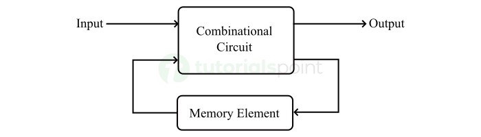
From this diagram, it is clear that an asynchronous sequential circuit is similar to a combinational logic circuit with a feedback mechanism.
Asynchronous sequential circuits are mainly used in applications where the clock signals are not available or practical to use. For example, in conditions when speed of the task execution is important.
Asynchronous sequential circuits are relatively difficult to design and sometimes they produce uncertain output.
The ripple counter is a common example of asynchronous sequential circuit.
Synchronous Sequential Circuit
A synchronous sequential circuit is a type of sequential circuit in which all the memory elements are synchronized by a common clock signal. Hence, synchronous sequential circuits take a clock signal along with input signals.
In synchronous sequential circuits, the duration of the output pulse is equivalent to the duration of the clock pulse applied. Take a look at the block diagram of a typical synchronous sequential circuit −
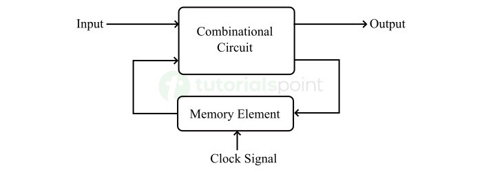
In this figure, it can be seen that the memory element of the sequential circuit is synchronized by a clock signal.
The major disadvantage of the synchronous sequential circuits is that their operation is quite slow. This is because, every time the circuit has to wait for a clock pulse for the operation to take place. However, the most significant advantage of synchronous sequential circuits is that they have a reliable and predictable operation.
Some common examples of synchronous sequential circuits include counters, registers, memory units, control units, etc.
Sequential Circuits vs. Combinational Circuits
Given below is a list of some of the main advantages of using sequential circuits over combinational logic circuits −
- Sequential circuits can retain the operation history which is important in various applications like data storage, feedback control systems, etc.
- Sequential circuits exhibit dynamic behavior and can execute complex operation in real time.
- Sequential circuits comprise a feedback mechanism which improves the stability and optimizes the system performance.
- Synchronous sequential circuits use a common clock signal for synchronization that ensures reliable operation of the circuit.
- Sequential circuits can perform more complex operations using simpler circuit designs than combinational circuits. Hence, their hardware complexity is lesser.
Disadvantages of Sequential Circuits
Sequential circuits do have several disadvantages too. Some of the key disadvantages of using sequential circuits are listed below −
- Sequential circuits have higher propagation delay because the input signal passes through multiple stages of logic circuits and memory elements.
- Sequential circuits are relatively complicated and time taking process to design and analyze.
- Sequential circuits require a proper synchronization and clock distribution to work as intended.
- As compared to combinational circuits, sequential circuits consume relatively more power due to complex design and use of additional components like clock and memory element.
Applications of Sequential Circuits
Sequential circuits are used in a wide range of applications in the field of digital electronics.The following are some common examples of applications of sequential circuits −
- Sequential circuits are used in digital counters employed in applications like frequency division, event counting, time keeping, and more.
- Sequential circuits are also used in digital memory devices like flip-flops, registers, etc. to store and retrieve data.
- Sequential circuits are used to design control circuits in digital systems.
- Sequential circuits play an important role in sequential logic and state-based data processing operations.
- Sequential circuits are also used in automation systems to control the operation of machines based on predefined logics.
- In communication systems, sequential circuits are used to implement communication protocols and data transmission standards.
Conclusion
Sequential circuits are important components in digital electronic systems. A sequential circuit is nothing but a combination of combinational logic circuit and a memory element, where the memory element is connected in a feedback mechanism with the combinational circuit.
The most important thing to be noted about sequential circuits is that their output is determined by both present inputs and previous inputs and outputs.
Sequential circuits are used to design complex digital systems that can perform advance operations like real-time data processing, storage and transmission of data, counting events, and more.